THE STRUCTURAL AND MAGNETIC PROPERTIES OF MNP FILMS AND NANOCRYSTALS
SEYYED NIMA NATEGHI
D´EPARTEMENT DE G´ENIE PHYSIQUE ´
ECOLE POLYTECHNIQUE DE MONTR´EAL
TH`ESE PR´ESENT´EE EN VUE DE L’OBTENTION DU DIPL ˆOME DE PHILOSOPHIÆ DOCTOR
(G ´ENIE PHYSIQUE) MAI 2014
c
´
ECOLE POLYTECHNIQUE DE MONTR´EAL
Cette th`ese intitul´ee :
THE STRUCTURAL AND MAGNETIC PROPERTIES OF MNP FILMS AND NANOCRYSTALS
pr´esent´ee par : NATEGHI Seyyed Nima
en vue de l’obtention du diplˆome de : Philosophiæ Doctor a ´et´e dˆument accept´ee par le jury d’examen constitu´e de :
M. MEUNIER Michel, Ph.D., pr´esident
M. M ´ENARD David, Ph.D., membre et directeur de recherche M. MASUT Remo A., Ph.D., membre et codirecteur de recherche M. MOUTANABBIR Oussama, Ph.D., membre
ACKNOWLEDGMENT
I would like to thank my advisers, David M´enard and Remo Masut, for their consistent support and inspiration. It was a pleasure working with these two brilliant scientists.
I would also like to thank Arthur Yelon and Patrick Desjardins for fruitful discussions and helpful suggestions.
I thank the members of the jury, Michel Trudeau, Michel Meunier, and Oussama Mouta-nabbir for evaluating this thesis and for their constructive comments.
I would like to thank Samuel Lambert-Milot for training me to use MOCVD and for provi-ding samples, which have been studied in this thesis.
I would like to thank Jelle Demeulemeester and Annie L´evesque for texture measurements of my samples.
I thank J¨oel Bouchard for his wonderful job in maintaining the MOCVD lab, and Jean-Phillipe Masse for his help in TEM imaging and sample preparation. I also thank Nicole MacDonal, Martin Chicoine, and Louis Godbout for helping me in TEM sample preparation.
I thank all my colleagues and friends, especially Christian Lacroix, Gabriel Monette, Elyse Adam, Louis-Phillipe Carignan, Nicolas Schmidt, Amir Roohi, Saman Choubak, and Foad Mehdizadeh for their support and helpful discussions.
And finally I thanks my wonderful parents, my brother and sister, and Debbie, my lovely girlfriend for their continuous support and endless love.
R´ESUM´E
Les semi-conducteurs magn´etiques h´et´erog`enes constitu´es de nano-aimants de pnictures de mangan`ese incorpor´es dans des matrices de semi-conducteurs ont des applications magn´ eto-´
electroniques et magn´eto-opto´electroniques potentielles tel que la magn´etor´esistance g´eante et les effets magn´etooptiques g´eants en raison de leurs fonctionnalit´es magn´etiques. Parmi ces mat´eriaux, les syst`emes h´et´erog`enes avec des temp´eratures de Curie ´elev´ees, comme MnSb, MnAs et MnP, ont fait l’objet de nombreuses ´etudes.
´
Etant donn´e que la texture des nanoagr´egats affecte fortement les fonctionnalit´es magn´ e-tiques des semi-conducteurs h´et´erog`enes, nous devons avoir un contrˆole sur la structure et la texture du syst`eme afin de r´ealiser les fonctions magn´etiques souhait´ees. Par cons´equent, il est n´ecessaire de comprendre les propri´et´es de l’h´et´erostructure en fonction de sa structure.
Les nanoparticules de MnP ferromagn´etiques encastr´ees dans une matrice de phosphure de gallium (GaP), GaP:MnP, crues par ´epitaxie en phase vapeur (MOVPE) ont ´et´e ´etudi´ees comme un syst`eme mod`ele pour v´erifier `a quel niveau la texture pouvait ˆetre pr´e-conditionn´ee par synth`ese. Malgr´e les ´etudes d´etaill´ees sur la fa¸con dont certains ´el´ements structuraux (par exemple la taille des nanoparticules) peuvent ˆetre contrˆol´es par les param`etres de croissance (par exemple la temp´erature de croissance), la complexit´e de ces syst`emes n’a pas permis de r´esoudre cette d´ependance.
L’objectif g´en´eral de ce travail est de comprendre le m´ecanisme de la croissance, de s´ elec-tion de la texture du MnP dans le GaP et comment la texture pourrait ˆetre conditionn´ee par les param`etres de croissance. Pour atteindre notre objectif, nous avons choisi d’´etudier un syst`eme moins complexe, des couches minces de MnP crues sur substrat de GaP, afin d’ap-profondir notre compr´ehension du m´ecanisme de croissance et d’´evolution de la texture des h´et´erostructures. La comparaison de l’´evolution de la texture de couches minces et de celle des h´et´erostructures nous aide `a comprendre le rˆole de la matrice de GaP, ce qui pourrait conduire `a la conception de structures avec les propri´et´es souhait´ees.
Un autre objectif de ce travail est de d´evelopper une m´ethode simple pour d´eterminer la taille magn´etique des nanoparticules de MnP ainsi que leur distribution. Puisque notre sujet d’int´erˆet porte sur la texture et la structure magn´etique des nanoparticules, la taille magn´ e-tique, par opposition `a la taille physique, des nanoparticules est la composante structurale pertinente `a ´etudier. Il n’existe pas dans la litt´erature de mod`ele coh´erent pour d´eterminer la distribution de la taille d’un ensemble de nanoparticules dont certaines sont superparama-gn´etiques et d’autres ferromagn´etiques, tel que les nanoparticules de MnP dans le GaP.
rayons-X (rayons-XRD) et la microscopie ´electronique (EM). Nous avons montr´e que la combinaison des figures de pˆoles depuis l’XRD et des diagrammes de diffraction des ´electrons obtenus `a partir de la microscopie ´electronique est avantageuse pour analyser la texture, compar´e `a chacune des techniques prise individuellement.
L’´etude de la dur´ee de la croissance et de l’´evolution de la temp´erature de la texture des couches de MnP nous a permis d’observer que : (1) les grains de MnP croissent partiellement `
a l’int´erieur du GaP, un ph´enom`ene connu sous le nom de croissance endotaxiale, (2) le GaP a souvent une surface convexe entre deux grains endotaxiaux de MnP, (3) les grains de MnP se forment dans un certain nombre d’orientations cristallographiques (´epitaxiales et axio-taxiales), (4) les grains MnP avec diff´erentes orientations cristallographiques ont diff´erentes facettes de la surface libre et diff´erentes profondeurs de diffusion, (5) la texture axiotaxiale domine `a des temp´eratures de croissance plus ´elev´ees.
Ces observations nous am`enent `a d´evelopper un mod`ele semi-quantitatif pour d´ecrire la croissance endotaxiale de grains de MnP. La surface convexe entre deux grains endotaxiaux sugg`ere que la croissance se produit `a travers la diffusion externe (out-diffusion) des atomes de gallium `a l’interface GaP/MnP, qui pourrait recristalliser par recombinaison avec les atomes de phosphore fournis en phase vapeur au cours de la croissance. La recristallisation d’´el´ement diffus´e de la colonne III a ´et´e observ´ee dans des syst`emes similaires (MnSb sur GaSb et MnSb sur InP). Les atomes de mangan`ese remplacent les atomes de gallium diffus´es et le MnP croit endotaxialement.
Compte tenu de l’´energie du syst`eme pendant la croissance de la couche mince (´energie libre de surface, l’´energie de l’interface, et l’´energie de contrainte), la croissance endotaxiale des grains de MnP forme des configurations o`u la surface de contact entre GaP et MnP tend `
a augmenter. Ceci favorise l’´energie de contrainte et d’interface du syst`eme par rapport `a l’augmentation de la surface libre du MnP.
`
A partir de l’´etude de la dur´ee de la croissance et de l’´evolution des profondeurs en-dotaxiales de grains MnP de diff´erentes orientations cristallographiques en fonction de la temp´erature, nous avons extrait les coefficients de diffusion (de l’ordre de 10−14cm2/s) et l’´energie d’activation (0, 6 ± 0, 2 eV) du processus de diffusion externe mentionn´ee ci-dessus (dans la gamme de temp´erature 550 − 650◦C). La valeur des coefficients de diffusion est au moins trois ordres de grandeur sup´erieure `a celle de la diffusion volumique du mangan`ese dans le GaP et l’´energie d’activation est un ordre de grandeur plus petite. Comme il n’y a pas de dislocations observ´ees dans nos ´echantillons, nous avons propos´e que ce processus de diffusion se produit par diffusion externe du Ga `a l’interface MnP/GaP `a travers des sites vacants qui pourraient exister en raison de la diff´erente structure cristalline du MnP et du GaP.
En comparant la texture des couches minces de MnP aux ´epicouches de GaP:MnP, nous avons r´ealis´e qu’il y a davantage de familles d’orientation ´epitaxiales et axiotaxiales pour le MnP dans les couches minces que dans les ´epicouches. Compte tenu de la maturation des nanoparticules (qui n’a pas ´et´e consid´er´ees initialement dans l’analyse du d´eveloppement de la texture) en cons´equence `a la diffusion du mangan`ese dans le GaP, nous avons sugg´er´e que la texture selectionn´ee dans les ´epicouches est similaire `a celle des couches minces de MnP au stade pr´ecoce de la croissance. Certaines familles d’orientations ´epitaxiales et axiotaxiales, qui ont ´et´e observ´ees dans les couches minces, disparaissent ´eventuellement dans les ´epicouches pendant le processus de maturation. Ceci a ´et´e attribu´e `a l’exc`es d’´energie d’interface et de contrainte gard´e au sein des cristaux (les nanoagr´egats), ce qui limite la poursuite de la croissance de ces familles d’orientation et de la texture axiotaxiale.
L’importance de la diffusion du mangan`ese dans le GaP a ´et´e r´ev´el´ee par l’´etude des h´et´erostructures de GaP/MnP/GaP et GaP/GaP:MnP/GaP. Le coefficient de diffusion du mangan`ese dans le GaP a ´et´e estim´e `a 4, 0 ± 0, 3 × 10⁻¹⁵ (cm2/s) `a 650◦C, ce qui est de deux
ordres de grandeur plus grand que la valeur r´epertori´ee pour la diffusion du mangan`ese dans le GaP. La diffusion accrue a ´et´e attribu´ee `a la concentration de d´efauts de structure dans les couches de GaP.
L’analyse de ces observations nous am`ene une compr´ehension accrue des ph´enom`enes inh´ e-rents aux processus de croissance comme la s´election et le d´eveloppement de la texture dans les semi-conducteurs magn´etiques h´et´erog`enes. Cependant, ces mˆemes observations confirment combien il est difficile de contrˆoler la texture de l’h´et´erostructure.
Enfin, en utilisant le concept de processus de renversement de l’aimantation thermique-ment activ´e, nous avons d´evelopp´e une m´ethode simple pour d´eterminer la taille magn´etique des nanoparticules de MnP ainsi que leur distribution. Notre m´ethode permet de construire l’histogramme de la taille magn´etique des nanoparticules `a partir de la mesure d’aimantation isor´emanente, et par cons´equent de trouver la distribution de la taille magn´etique d’un en-semble de nanoparticules. Nos r´esultats montrent que la taille magn´etique des nanoparticules est de fa¸con significative (20 `a 50 %) plus petite que la taille physique apparente obtenue `
a partir de l’analyse d’image EM. Cela pourrait ˆetre dˆu `a des d´eficiences des techniques ´
electromagn´etiques dans la d´etermination de la taille des nanoparticules non sph´eriques, `a une possible couche morte magn´etique recouvrant les nanoparticules, ou encore `a la sur-simplification du mod`ele magn´etique dans l’extraction de la distribution de la taille.
ABSTRACT
Heterogeneous magnetic semiconductors consisting manganese pnictide nanomagnets em-bedded in semiconductor matrices have potential magnetoelectronic and magnetooptoelec-tronic applications due to their enhanced magnetic functionalities, such as Giant Magneto-Resistance (GMR) and Giant Magneto-Optical (GMO) Kerr and Faraday effects. Among these, heterogeneous systems with higher Curie temperatures, such as manganese antimonide, manganese arsenide, and manganese phosphide (MnP) have been the focus of many studies. Since the texture of the nanoclusters highly affects the magnetic functionalities of the heterogeneous semiconductors, in order to achieve the desired magnetic functionalities we need to have a control over the structure and texture of the system. Hence, it is necessary to understand the properties of the heterostructure in relation to its structure.
Ferromagnetic MnP nanoclusters embedded in gallium phosphide (GaP) matrix, GaP:MnP, grown by Metal-Organic Vapor Phase Epitaxy (MOVPE) has been studied as a model system to verify to what level the texture could be pre-conditioned by synthesis. Despite the valuable achievements of the studies on how some structural components (e.g. size of nanoclusters) can be controlled by growth parameters (e.g. growth temperature), the complexity of the structure did not allow to fully exploit this matter.
The general objective of this work is to understand the growth mechanism and texture selection of MnP on GaP and how the texture could be pre-conditioned by growth. To achieve our goal we chose to study a less complex system, MnP thin films grown on GaP, in order to expand the limits of our understanding on the growth mechanism and texture evolution of the heterostructure systems. Comparing the texture evolution of thin films and heterostructures helps us understand the role of the surrounding GaP matrix on texture, which may potentially lead to designing structures with desired properties.
Another objective of this work is to develop a simple method to determine the magnetic size distribution and magnetic size of MnP nanoclusters. Since our topic of interest deals with the texture and structure of magnetic nanoparticles, the magnetic size of the nanoparticles is the relevant structural component to study, rather than their apparent physical size. How-ever, there is a lack of a consistent model to determine the magnetic size distribution of an assembly of superparamagnetic and ferromagnetic nanoparticles (such as MnP nanoclusters in GaP:MnP) in the literature.
To analyze the texture of MnP films we have used X-ray diffraction (XRD) and electron microscopy (EM) techniques. We have shown that combining the XRD pole figures and electron diffraction patterns obtained from EM makes a much stronger tool to analyze the
texture compared to each of the techniques applied alone.
Studying the growth time and temperature evolution of the texture of MnP thin films we observed: (1) MnP grains partially grow inside GaP, a phenomenon known as endotaxial growth, (2) GaP often has a convex surface between two endotaxial MnP grain, (3) MnP grains form in a specific number of crystallographic orientations (epitaxial and axiotaxial), (4) MnP grains with different crystallographic orientations have different free surface facets and different diffusion depths, (5) the axiotaxial texture dominates at higher growth temperatures. These observations lead us to develop a semi-quantitative model to describe the endotaxial growth of MnP grains. Convex GaP surface between two endotaxial grains suggest that the endotaxial growth occurs through the out-diffusion of Ga atoms at GaP/MnP interface, which could recrystallize at the surface through recombination with P atoms provided during the growth. The recrystallization of the out-diffused element III has been observed in similar systems (MnSb on GaSb and MnSb on InP), as well. Mn atoms replace the out-diffused Ga atoms and MnP grows endotaxially.
Considering the energy of the system as the film grows (free surface energy, interface energy, and strain energy), the endotaxial growth of MnP grains indicates that increasing the contact surface area between GaP and MnP, which enhances the interface and strain energy of the system is favored over increasing the free surface area of MnP.
Studying the growth time and temperature evolution of the endotaxial depths of MnP grains with different crystallographic orientations, we have extracted the diffusion coefficients (order of 10−14cm2/s) and the activation energy (0.6±0.2 eV) of the above mentioned diffusion
process (in the temperature range 550−650◦C). The values of diffusion coefficients are at least three orders of magnitude larger than those of Mn bulk diffusion in GaP and the activation energy is one order of magnitude smaller. Since there are no dislocations observed in our samples, we suggested this large diffusion process to occur through Ga self-diffusion at the MnP/GaP interface through vacant sites that could exist due to different crystal structure of MnP and GaP.
By comparing the texture of MnP films and GaP:MnP epilayers, we realized that there are more epitaxial orientation families and axiotaxial textures in the films than in the epilayares. Considering the ripening of the nanoclusters (which was not considered initially in the texture development analysis) due to diffusion of Mn in GaP, we suggested that the texture selection in the GaP:MnP epilayers is similar to that of MnP thin films at the early stage of growth. Some epitaxial orientation families and axiotaxial textures, which have been observed in thin films disapper in the epilayers during the ripening process. This has been attributed to the excess interface/strain energies in the buried crystals (nanoclusters), which limits the further growth of those orientation families and axiotaxial features.
The significance of Mn diffusion in GaP has been revealed by studying the GaP/MnP/GaP and GaP/GaP:MnP/GaP heterostructures. The diffusion coefficient of Mn inside GaP has been estimated to be 4.0 ± 0.3 × 10⁻¹⁵ (cm2/s) at 650◦C, which is two orders of magnitude
larger than the reported value for Mn diffusion in bulk GaP. The enhanced diffusion has been attributed to large concentration of structural defects in GaP layers.
These observations brought us one step closer to understand the texture selection and development in heterogeneous magnetic semiconductors. However, they clarified how chal-lenging it is to control the texture of the heterostructure.
Finally, using the concept of thermally activated magnetization reversal process, we have developed a method to extract the magnetic size distribution and magnetic size of MnP nanoclusters in GaP:MnP. Our method enables us to build the magnetic size histogram of the nanoclusters from the isoremanent magnetization measurements, and consequently find the magnetic size distribution and magnetic size by fitting the histogram using known mathematical functions. Our results show that the magnetic size of the nanoclusters is significantly (20-50%) smaller than their apparent physical size obtained from EM image analysis. This could be attributed to deficiencies of EM techniques in determining the size of the non-spherical nanoparticles from their projected area, possible magnetic dead layer covering the nanoclusters, or the over simplification of the magnetic model in extracting the size distribution.
TABLE OF CONTENTS DEDICATION . . . iii ACKNOWLEDGMENT . . . iv R´ESUM´E . . . v ABSTRACT . . . viii TABLE OF CONTENTS . . . xi
LIST OF TABLES . . . xiv
LIST OF FIGURES . . . xvi
LIST OF APPENDICES . . . .xxvii
NOMENCLATURE . . . .xxviii
CHAPTER 1 INTRODUCTION . . . 1
1.1 Magnetic semiconductors . . . 1
1.2 Growth techniques . . . 2
1.3 Effect of texture on GMO and GMR responses . . . 2
1.4 Motivation, general objective, and choice of material . . . 3
1.5 Organization of the thesis . . . 5
CHAPTER 2 Texture evolution in polycrystalline thin films . . . 6
2.1 Different types of texture . . . 7
2.2 Texture development in polycrystalline thin films . . . 7
2.2.1 Pre-coalescence texture development . . . 9
2.2.2 Texture development during coalescence . . . 11
2.2.3 Time and Temperature evolution of the texture of thin films . . . 12
2.3 Endotaxial growth . . . 14
CHAPTER 3 Experimental techniques . . . 18
3.1 MOVPE growth of MnP and GaP:MnP films and multilayers . . . 18
3.2.1 Transmission electron microscopy . . . 21
3.2.2 Dislocation imaging . . . 23
3.2.3 TEM sample preparation . . . 24
3.2.4 Scanning electron microscopy . . . 26
3.3 X-ray diffraction pole figures . . . 27
3.4 Vibrating sample magnetometer (VSM) . . . 33
CHAPTER 4 Texture evolution of polycrystalline MnP films grown on GaP (100) . . 36
4.1 Introduction . . . 36
4.2 Growth time evolution of MnP films grown on GaP (100) . . . 38
4.2.1 MnP films grown at 550◦C . . . 38
4.2.2 MnP films grown at 650◦C . . . 45
4.3 Growth temperature evolution of MnP films grown on GaP (100) . . . 51
4.4 Discussion . . . 58
4.4.1 Crystallographic orientation of MnP grains grown on GaP (100) . . . . 60
4.4.2 Free surface facets of MnP grains . . . 62
4.4.3 Endotaxial growth of MnP grains on GaP . . . 62
4.4.4 Could endotaxial growth favor axiotaxial texture ? . . . 63
4.4.5 Growth rates . . . 64
4.5 Endotaxial growth model . . . 65
CHAPTER 5 Texture of MnP films vs. MnP nanoclusters . . . 69
5.1 Texture of GaP:MnP epilayers . . . 69
5.1.1 GaP:MnP epilayers grown at 550◦C . . . 70
5.1.2 GaP:MnP epilayer and MnP film grown at 600◦C . . . 70
5.1.3 GaP:MnP epilayers and MnP films grown at 650◦C . . . 71
5.1.4 Samples grown at 700◦C . . . 74 5.2 Multilayer samples . . . 74 5.2.1 GMP-M10 (GaP/GaP:MnP/GaP (period =10)) . . . 74 5.2.2 MnP-M17 (GaP/MnP/GaP (period = 17)) . . . 76 5.3 Discussion . . . 78 5.4 Summary . . . 83
CHAPTER 6 Extracting the magnetic size distribution of an assembly of ferromagne-tic/superparamagnetic nanoparticles using magnetometry . . . 85
6.1 Introduction . . . 85
6.2.1 Demagnetization in the absence of applied magnetic field . . . 87
6.2.2 Remagnetization in the presence of applied magnetic field . . . 89
6.2.3 Volume distribution of particles . . . 91
6.3 Description of the method . . . 95
6.4 Application of the method to GaP:MnP . . . 99
6.4.1 Magnetic size distribution of GaP:MnP . . . 99
6.4.2 Validation of the method . . . 103
6.4.3 Magnetic size distribution of GaP:MnP grown at different temperatures 105 6.4.4 Discussion . . . 107
CHAPTER 7 Conclusion . . . 111
7.1 Summary of the work and principal contributions . . . 111
7.1.1 Texture selection in MnP films, nanocrystals, and multilayers . . . 111
7.1.2 Magnetic size distribution of MnP nanoclusters in GaP:MnP . . . 113
7.2 Suggestions for future work . . . 114
7.2.1 Energy terms and enhanced diffusion of Mn in GaP . . . 114
7.2.2 Controlling the texture . . . 114
7.2.3 Magnetic properties of an individual MnP nanocluster studied by elec-tron holography . . . 116
REFERENCES . . . 117
LIST OF TABLES
Table 1.1 Influence of the structure and texture of nanoclusters on MO and MR responses. . . 3 Table 3.1 List of samples grown on GaP (100) substrates by the procedure
des-cribed in the text. . . 20 Table 3.2 List of MnP films grown on glass substrates. The growth procedure is
described in the text. . . 20 Table 3.3 List of parameters used for the growth of samples studied in this thesis,
as well as their range of values. . . 21 Table 4.1 Average effective diameter and mean effective diameter of MnP crystals
grown at 550◦C for different growth times, as well as their standard deviations and aspect ratios. . . 38 Table 4.2 Average normal growth rate of the samples grown at 550◦C compared
to their lateral growth rates. . . 41 Table 4.3 Epitaxial alignments of MnP grains in MnP-550-15 obtained from pole
figure analysis by decreasing order of population weight. The last co-lumns indicate the least value of strain, respectively calculated for each alignment using equation 4.2, as well as the integers m and n (described in the text). . . 45 Table 4.4 Average effective diameter of primary MnP grains grown at 650◦C for
different growth times, as well as their standard deviations and aspect ratios. . . 46 Table 4.5 Average normal growth rate of the primary grains grown at 650◦C
compared to their lateral growth rates. . . 47 Table 4.6 Observed epitaxial alignments of the MnP grains for the three samples
grown at 650◦C for the growth times indicated in the table. These orientations are obtained from FFT (MnP-650-5) and SAED patterns (MnP-650-15 and MnP-650-30). . . 50 Table 4.7 Average effective diameters of the grains in MnP films grown for 15
minutes at different temperatures. . . 51 Table 4.8 Average normal growth rate of the primary grains grown at different
temperatures compared to their lateral growth rates. The sample MnP-750-15 was not available to determine its effective diameter and lateral growth rate from SEM micrographs. . . 51
Table 4.9 Epitaxial alignments of MnP grains in MnP-550, MnP-600, and MnP-650. 58 Table 4.10 The angles between MnP [020] with GaP [-11-1] (α1), MnP [-11-1] with
GaP [11-1] (α2), and MnP [-13-1] with GaP [02-2] (α3) directions in
three MnP grains of MnP-600-15. . . 60 Table 5.1 List of all orientation families (mostly alignments with low-index GaP
planes) in the GaP:MnP epilayers and MnP film grown at 650◦C. . . . 73 Table 6.1 Anisotropy fields and saturation magnetization of GaP:MnP at
dif-ferent temperatures Lacroix (2010). . . 93 Table 6.2 The angles θci and φci for orientations O3 to O6 Lacroix (2010). . . 102
Table 6.3 Extracted parameters from the lognormal fit of magnetic size histogram of GMP-650-45 obtained at 240, 260, and 280 K. . . 104 Table 6.4 Mean effective diameter (m) and standard deviation (s) extracted from
the lognormal fit of the magnetic size histogram and TEM size histogram.106 Table A.1 Average maximum depth of Mn diffusion in GaP <11-1>, d<111>, for
MnP grains grown at 550◦C with MnP {121} || GaP {100}. . . 123 Table A.2 d<111> (nm) and the obtained diffusion coefficients (D<111>) of Mn in
GaP. The data presented without error are obtained from only one grain. The diffusion coefficient for MnP {111} || GaP (100) is obtained from four grains of MnP-650-15, using the diffusion equation d =√Dt, where d is the average in-diffusion depth of Mn and t is the growth time.124 Table A.3 Diffusion coefficient of Mn in GaP along <111> at different growth
temperatures below the congruent temperature of GaP. . . 124 Table A.4 Average maximum endotaxial depth of MnP in GaP along GaP [100],
d, for MnP grains grown at 550◦C and 650◦C. . . 127 Table A.5 Portion of the GaP substrate, which is covered by MnP films grown at
LIST OF FIGURES
Figure 2.1 Schematic representation of the interface of axiotaxial alignments of NiSi film grown on Si (110), as reported in Ref. (Detavernier et al., 2003). The d-spacings of the four planes shown in the figure at the interface (dint) almost match the d-spacing of Si (220) (d) at the
inter-face. However, only NiSi (211) and (202) || Si (220) are axiotaxy axes, since the normals to their planes make the same angle (χ) with the interface as the normal to Si (220) plane does (χ = 45◦), thus creating a periodic interface. . . 8 Figure 2.2 Growth stages of a polycrystalline film on a polycrystalline or
amor-phous buffer layer : a) nucleation, b) crystal growth, c, d) coalescence and grain growth to form a continuous film, e) thickening of the conti-nuous film. In the image the light circles are the adatoms and the dark circles are impurity atoms. This schematic representation is adapted from Ref. (Barna et Adamik, 1995). . . 9 Figure 2.3 Hemispherical cap shape particle that partially wets the substrate. γf,
γs, and γi are the surface energy of the particle (J/m2), surface energy
of the substrate (J/m2), and the particle-substrate interface energy (J/m2), respectively. α, β, and δ are the possible axes of rotation of
the particle. θc is the contact angle and r? is the critical radius for
the nucleus formation. This schematic representation is adapted from Ref. (Thompson et Carel, 1995). . . 10 Figure 2.4 Basic structure zone model describing the temperature evolution of the
texture of thin films. Ts and Tm in the horizontal axis represent the
temperature of the substrate and the melting point of the bulk film. The figure is taken from Ref. (Barna et Adamik, 1995). . . 13 Figure 2.5 Real structure zone model that considers the level of impurity, as well
as growth temperature to describe the texture evolution of thin films : a) Low impurity (Cimp < 0.5%), b) medium impurity (Cimp≈ 1%), and
c) high impurity (Cimp > 10 %) level (Barna et Adamik, 1995). . . 14
Figure 2.6 Cross-sectional TEM images revealing the endotaxial growth of MnSb on GaSb at a) 380 ± 10◦C and b) 465 ± 10◦C. The images are taken from Ref. (Braun et al., 2007). . . 16
Figure 2.7 a) Braun’s proposed mechanism for endotaxial growth of MnSb on GaSb, and b) similar growth mechanism proposed for endotaxial growth of MnSb on InP. Dashed arrows indicate elemental fluxes, while solid arrows show the growth direction. The figure is taken from S. Hatfield’s thesis (Hatfield, 2006). . . 17 Figure 3.1 Schematics of the MOVPE reactor dedicated to the growth of
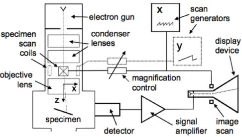
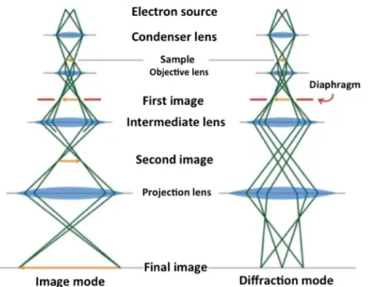
com-pounds containing transition metals, such as Mn. The image is taken from Ref. (Lambert-Milot, 2012). . . 18 Figure 3.2 Schematic representation of a TEM. The figure is taken from Ref.
Lambert-Milot (2012). . . 22 Figure 3.3 a) Cross-sectional TEM image of a MnP grain grown at 600◦C on
GaP, b) the SAED pattern of GaP substrate and MnP grain, and c) determined normal direction to GaP and MnP planes. The diameter of the aperture hole to obtain the SAED pattern is 120 nm. According to (c), we assigned the alignment MnP [-13-1] || GaP [02-2] to this grain. . 24 Figure 3.4 a) Cross-sectional TEM image of MnP-650-15 taken at GaP [011] zone
axis along g [200]. b) The diffraction condition, where only GaP {200} planes diffract. . . 25 Figure 3.5 Few steps of TEM sample preparation using FIB technique. a)
Sand-wich of two samples and the tungsten layer deposited on the surface, b) ion milling, lamella preparation, and microprobe welding, c) trans-ferring the lamella to copper grid. . . 26 Figure 3.6 Schematic representation of an SEM. The image is taken from Ref.
Eger-ton (2005). . . 27 Figure 3.7 Plan view SEM image of MnP film grown on GaP (100) at 600◦C
showing polycrystalline MnP grains on the surface. . . 28 Figure 3.8 Definition of reciprocal space coordinates 1/ dhkl , ψ and φ associated
to a crystalline material sample. . . 29 Figure 3.9 Configuration of XRD pole figure measurement. a) Incident (S0) and
diffracted (S1) beam and their angle with sample’s plane, b) geometry
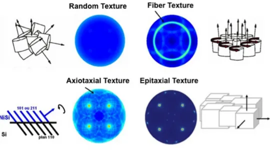
of the sample holder and illustration of angles, c) experimental setup to obtain reciprocal space map with a synchrotron source, and d) different types of detectors and their corresponding scan modes. . . 30 Figure 3.10 Different types of texture and their corresponding pole figures. This
Figure 3.11 Position of different planes normal on the reciprocal space map of GaP. This reciprocal space map is obtained by a projection of a surface in 3D to a plane. The image is taken from (Lambert-Milot, 2012). . . 31 Figure 3.12 MnP (111) Pole figure of MnP-650-15. The blue color shows the
lo-west intensity and the red shows the highest. The spots with higher intensity correspond to epitaxial grains, while the arc corresponds to axiotaxial grains. The dark blue color on the right side of the pole figure corresponds to the angular portion that has not been measured. . . 32 Figure 3.13 Schematic representation of a VSM measurement. . . 34 Figure 3.14 The IRM response of GMP-650-45 to the magnetic field (in-plane)
ap-plied at T = 280 K. . . 35 Figure 4.1 a) Cross-sectional TEM micrograph of GMP-650-5, showing the
for-mation of GaP (111) facets. White arrows show the MnP nanoclusters that form on GaP (111) facets. . . 36 Figure 4.2 Schematic representation of the growth model describing the time
evo-lution of the texture of GaP:MnP epilayers. Symbols with different colors inside the nanoclusters correspond to a specific family of orien-tation, described in Refs. (Lambert-Milot, 2012),(Lambert-Milot et al., 2012). The image is taken from Ref. (Lambert-Milot, 2012). . . 37 Figure 4.3 Plan view SEM micrographs of a) MnP-550-1.5, b) MnP-550-5, and
c) MnP-550-15 showing formation of polycrystalline films. The sample grown for 1.5 min appears to be in the pre-coalescence stage, while the crystals of the samples grown for longer times are in contact with each other and most likely are in the coalescence stage. . . 39 Figure 4.4 Size histogram of a) MnP-550-1.5, b) MnP-550-5, and c) MnP-550-15.
The size distribution of MnP-550-1.5 looks unimodal, which is not the case for MnP-550-5 and MnP-550-15, as a comparison with the best lognormal fit (obtained from Igor pro software) indicates. . . 40 Figure 4.5 Cross-sectional TEM images of a) MnP-550-1.5, b) MnP-550-5, and c)
MnP-550-15. The white line in (a) shows the GaP buffer layer/substrate interface. MnP grows endotaxially on GaP, even at an early stage of growth, as shown in (a). We also observe that samples with longer growth times have larger endotaxial depths. . . 40
Figure 4.6 a) HR-TEM image of a MnP crystal in MnP-550-1.5 and b) its FFT pattern. Analyzing the FFT pattern (shown in (b)), we assigned the MnP {121} || GaP (200) the alignment to this grains. Moreover, we determined MnP (010), (111), and (101) surface facets, as shown in the HR-TEM image. The long white line shows the surface of the GaP buffer layer ( ≈ 200 nm thick). We also observe that this crystal partly grew inside the GaP buffer layer. . . 41 Figure 4.7 HR-TEM image of five MnP grains in MnP-550-1.5. We could not
de-termine the orientation of grain A, since it completely grew inside GaP and we do not clearly observe its planes. Grains D and E have the same alignment, namely MnP {121} || GaP (200). . . 42 Figure 4.8 a) A trapezoidal crystal in MnP-550-5 with MnP {121} || GaP (200),
and b) an elongated crystal in MnP-550-5 with MnP {110} || GaP (200). The two crystals have different surface facets (except for MnP {111} facet). . . 42 Figure 4.9 Pole figures of MnP-550-15 obtained using a planar detector a) MnP
{020}, b) MnP {101}, and c) MnP {211}. The bright spots indicate epitaxial alignments, while partial arcs/lines indicate partial axiotaxy. 44 Figure 4.10 Plan view SEM micrographs of a) 650-5, b) 650-15, c)
MnP-650-30 show the formation of polycrystalline films, the grains of which grow larger in time. In (c) we observe the formation of long rods (≈ 2 µm) on top of primary grains. . . 46 Figure 4.11 Lateral size histograms of primary MnP grains of a) MnP-650-5, b)
MnP-650-15, and c) MnP-650-30 show a multimodal distribution. . . . 47 Figure 4.12 Cross-sectional TEM images of a) MnP-650-5, b) MnP-650-15, and c)
MnP-650-30, showing the endotaxial growth of the grains. Grains with longer growth times have a larger endotaxial depths. Nucleation and growth of secondary grains is observed in (b) and (c). We infer that secondary grains have a tendency to grow as long rods, as observed in MnP-650-30. . . 48 Figure 4.13 TEM micrograph of three nanorods in MnP-650-30 and their
corres-ponding SAED patterns. Two of the nanorods are growing faster in [002] direction, while the other one is elongated along [101]. . . 49 Figure 4.14 Plan view SEM images of MnP films grown at a) 550◦C, b) 600◦C, c)
650◦C, and d) 700◦C. e) Larger area of MnP-700-15, showing formation of very long nanorods. . . 52
Figure 4.15 Bright field cross-sectional TEM images of MnP films grown for 15 min at a) 550◦C, b) 600◦C, c) 650◦C, and d) 700◦C, and e) 700◦C. The white line in b) shows the GaP substrate/buffer layer interface. Formation of new grains on top of endotaxial primary grains is observed in (c), (d), and (e). . . 53 Figure 4.16 MnP 020 pole figure of MnP-650-15. The white arrows show the bright
spots located at ψ = 64 and φ = 0◦, 90◦, 180◦, and 270◦. These are the angular positions where we expect GaP {233} planes. This pole figure has been obtained using a linear detector. . . 54 Figure 4.17 MnP {101} and b) MnP {211} pole figures of MnP-650-15. In these
pole figures we observe bright spots and bright arcs/line segments that indicate epitaxial and partial axiotaxial alignments. These pole figures have been obtained using a planar detector. . . 55 Figure 4.18 MnP {211} pole figures of a) MnP-550-15, b) MnP-600-15, c)
MnP-650-15, d) MnP-700-MnP-650-15, e) MnP-750-15. The white arrows show the bright spots due to the artifacts of the experiment. For 700-15 and MnP-750-15 we only see bright arcs and lines that indicate axiotaxial texture, while the other samples have epitaxial and partial axiotaxial textures. The pole figures have been obtained using a planar detector. . . 56 Figure 4.19 MnP (020) pole figures of a) MnP-600-15 and b) MnP-650-15, as well
as MnP (111) pole figures of c) MnP-600-15 and d) MnP-650-15. We observe more features on the pole figures of 650-15 than MnP-600-15. The pole figures have been obtained using a linear detector. . . 59 Figure 4.20 Axiotaxial features on a) MnP (020) and b) MnP (111) pole figures of
MnP-650-15. The purple/green arcs on MnP (111) pole figure appear as lines on MnP (020) pole figure. As it is described in the text, we do not show the purple/green line in the MnP (020) pole figure. . . 59 Figure 4.21 SAED pattern of MnP grains with a) MnP (-13-1) || GaP (02-2), b)
MnP (-1-1-1) || GaP (200), and c) MnP (-11-1) || GaP (11-1) alignments are shown below their TEM micrographs. . . 61 Figure 4.22 Small bright spots that are very close to each other on the MnP (020)
of MnP-600-15. The region in the box is enlarged and presented on the right. The black arrows point to some of the bright spots on the seemingly axiotaxial line. This pole figure is obtained by a linear detector. 62
Figure 4.23 Schematic side view of GaP/MnP contact area in a) MnP crystal gro-wing on top of GaP and b) MnP crystal grogro-wing partially inside GaP. Red lines show the portion of MnP that is in contact with GaP. This indicates the larger contact area in the case of endotaxial growth. . . . 63 Figure 4.24 Two grains of MnP-650-15 with different orientation that have different
facets and different endotaxial depth. a) MnP {121} || GaP (200), en-dotaxial depth along GaP <111> = 57 nm, and b) MnP {110} || GaP (200) endotaxial depth along GaP <111> = 27 nm. The long white lines show the approximate position of where the surface of GaP buffer layer is deduced to be. . . 64 Figure 4.25 a) Initial stage of nucleation of MnP on GaP, b) Mn atoms replacing
the Ga atoms that are diffused to the surface, and c) endotaxial growth of MnP crystal and formation of a GaP bump at the surface. . . 65 Figure 4.26 Recrystallization of GaP at the surface, possibly from out-diffused Ga
atoms in MnP-600-15. . . 66 Figure 4.27 Semi-logarithmic graph of the diffusion coefficient (D) as a function of
(1000/T ) for our samples (average of all orientation families) and their corresponding linear fits, compared to Mn bulk diffusion reported in Ref. Kirillov et al. (1980). The extracted activation energy (∆E) and the pre-exponential factor (D0) in our samples are 0.45 ± 0.14 (eV)
and 1.03 ± 0.99 × 10⁻¹¹(cm2/s), respectively, compared to 4.7 (eV) and
2.1 × 10⁹(cm2/s) reported in Ref. Kirillov et al. (1980). The interface
and bulk diffusion coefficients of Mn in GaAs are also presented in the graph for comparison. . . 67 Figure 4.28 Cross-sectional TEM image of MnP-650-15 taken at GaP [1-12] zone
axis along g [1-11] and its corresponding diffraction paatern. No dislo-cations are observed in this image. . . 67 Figure 5.1 a) Plan-view SEM image of GaP grown at 600◦C shows its poor surface
quality. b) Presence of many structural defects revealed from the cross-sectional TEM micrograph of GMP-600-45. . . 71 Figure 5.2 a) MnP (020) and b) MnP (101) pole figures of GMP-650-15 (top)
compared to c) MnP (020) and d) MnP (101) pole figures of MnP-650-15 (bottom). More bright spots and partial arcs are observed in the pole figures of MnP-650-15, which indicates that there are more epitaxial and partial axiotaxial orientations in this sample compared to GMP-650-15. These pole figures are obtained using a linear detector. 72
Figure 5.3 Cross-sectional TEM images of GMP-M10. In (a) we see that the spa-cing between the first few layers is much less than that of the last layers, which indicates more Mn diffusion in GaP for the first few layers. In (b), at higher resolution, we highlight a 80 nm thick layer containing MnP nanoclusters, while the growth time should contain the nanoclusters to a 30 ± 5 nm thick layer. . . 75 Figure 5.4 Square of the diffusion length as a function of time in GMP-M10. The
slope of the line represents the diffusion coefficient of Mn in GaP to be 4.0 ± 0.3 × 10⁻¹⁵ (cm2/s). The error bars are roughly estimated. . . 76 Figure 5.5 Plan-view SEM image of a GaP layer (60 nm) grown at 650◦C that
has been grown on a 30 nm GaP:MnP layer (grown at 650◦C). The dark spots are the GaP surface pits. These pits are also observed in cross-sectional TEM images of GMP-650-1.5 in (Lambert-Milot, 2012),(Lambert-Milot et al., 2012). . . 77 Figure 5.6 Cross-sectional TEM images of MnP-M17, a sample grown at 650◦C
(GaP) and 550◦C (MnP) to nominally have 17 periods of 3 nm MnP and 50 nm GaP. We observe formation of larger nanoclusters close to the buffer layer/epilayer interface. We also observe formation of GaP with different crystallographic orientations and structural defects in this sample. . . 78 Figure 5.7 a) ED pattern, b) GaP (111), and c) GaP (200) pole figures of
MnP-M17. The presence of many bright spots on the ED pattern and pole figures suggest that in this sample GaP crystals grow with different crystallographic orientations. The yellow arrows show the expected an-gular positions of GaP (111) and (200) planes of the substrate. The red and white arrows correspond to angular positions of GaP (111) and (200) planes of some GaP crystals that are differently oriented than the substrate, on which MnP nanoclusters nucleate (will be pre-sented in figure 6.11). These pole figures are obtained using a linear detector. . . 79 Figure 5.8 a) MnP (020) and b) MnP (101) pole figures of MnP-M17. The white
and red arrows in a) correspond to MnP {020} || GaP {100} (red circle) and MnP {020} || GaP {111} (lines) alignments for the nanoclusters that form on GaP crystals with different orientation than the substrate. The pole figures are obtained using a linear detector. . . 80
Figure 5.9 a) MnP nanoclusters embedded in GaP (GMP-650-1.5) compared to b) MnP crystal grown endotaxially on GaP (GMP-650-1.5). . . 80 Figure 5.10 Schematic representation of the ripening process in GaP:MnP. a)
Ini-tial stage of nucleation of a nanocluster. b) As the nanocluster grows, it ends up surrounded by GaP due to larger growth rate of GaP. c) When this nanocluster is completely buried in GaP, Mn atoms of this nanocluster may diffuse towards a neighboring nanocluster with lower energy (shown by the block arrow). In this representation we do not show the P atoms. . . 81 Figure 5.11 Schematic representation of nucleation of MnP nanocluster in
MnP-M17 (only three MnP layers are shown). The arrows show the direction of Mn diffusion from the crystals to the nanoclusters, that potentially occurs through structural defects present in this sample. . . 83 Figure 6.1 Magnetic energy of the system (vertical) as a function of the angle with
respect to the z-axis (horizontal). The minima of magnetic energy in the absence of external magnetic field (H0 = 0) are at -180◦ and 0◦,
corresponding to (↓) and (↑), respectively. . . 87 Figure 6.2 Schematic diagrams of the magnetic energy and its deep and shallow
minima in applied field H0. The figure shows the change in populations
of (↑) and (↓) a) right after the field is applied and b) some time (t0)
after it is applied. . . 90 Figure 6.3 a) Rapid variation of τ (V ) as a function of the diameter of MnP
nano-clusters in GMP-650-45 and b) rapid variation of the exponential term in Eq. (6.22) as a function of the diameter of the nanoclusters, for dif-ferent time constants (t = 1 s, 90 s, and 1 day). The exponential term could be fairly approximated with a step function. The energy barrier density of the clusters has been calculated at 260 K at zero applied field. The diameter has been calculated assuming spherical nanoclusters. . . 92 Figure 6.4 Isoremanent magnetization, temperature of experiment, and applied
magnetic field as a function of time during ZF C process and IRM measurement. . . 96 Figure 6.5 Bright field cross-sectional TEM image of GaP:MnP grown at 650◦C. . 99 Figure 6.6 Easy axes of magnetization (c-axis) of MnP nanoclusters with respect
Figure 6.7 Magnetic field H0 applied at an arbitrary angle θH with respect to GaP
[100]. The Hard (a-axis of MnP) and intermediate (b-axis of MnP) anisotropy fields of a MnP (orthorhombic with convention a > b > c) nanocluster are also shown in the figure. . . 101 Figure 6.8 a) 3D representation of the magnetic energy density of GaP:MnP at
H0 = 0. Points A, D, B, and C represent local minima, saddle point,
and maximum of the energy density, respectively. b) Contour graph of the magnetic energy density of GaP:MnP at H0 = 0. The points A,
B, C, D are the same as shown in part (a). The blue color represents the lowest and the red color indicates the highest value of the energy density. . . 102 Figure 6.9 3D representation of the magnetic energy density of GaP:MnP at H0 =
159kA/m(2000Oe). Points A, D, B, and C represent the local minima, saddle point, and maximum of the energy density, respectively. b) Same graph as in (a), but from a different point of view. c) Contour graph of the magnetic energy density of GaP:MnP at H0 = 159kA/m(2000Oe). . 103
Figure 6.10 The IRM response of GMP-650-45 at T = 280 K. . . 104 Figure 6.11 The magnetic size histogram of GMP-650-45 and its lognormal fit
ob-tained at a) 240 K, b) 260 K, and c) 280 K. . . 105 Figure 6.12 Magnetic hysteresis curve of GMP-650-45 obtained at 240 K, while the
magnetic field was applied parallel to sample’s normal (GaP [100]). The blue dots show the experimental data and the red line shows the result of simulation using the parameters presented in Table 6.3. . . 106 Figure 6.13 Magnetic size histogram obtained at T = 280 K (left) vs. physical size
histogram (right) of a) 600-45, b) 650-45, and c) GMP-700-45. . . 107 Figure A.1 A grain in MnP-600 with MnP {131} || GaP (111) alignment. The long
white line shows the expected GaP surface prior to growth of MnP. For this grain we measured d[100] = 43 nm and d[−11−1] = 76 nm. . . 123
Figure A.2 Square of the diffusion depth (d2
<111>) of MnP grains grown at with
MnP {121} || GaP (100) in GaP along <111> direction as a function of growth time (t). The slope of the line reveals the diffusion coefficient of D<111>= 1.31 ± 0.012 × 10⁻¹⁴(cm2/s). . . 124
Figure A.3 d<111> as a function of growth time for a) MnP {010} || GaP (111)
(D<111> = 1.4 × 10⁻¹⁴± 8.4 × 10⁻¹⁶(cm2/s)), b) MnP {110} || GaP
(200) (D<111> = 2.6 × 10⁻¹⁴± 1.7 × 10⁻¹⁵(cm2/s)), and c) MnP {121}
|| GaP (200) (D<111> = 3.8 × 10⁻¹⁴± 2.6 × 10⁻¹⁵(cm2/s)). Since we
only had two data points, we added the point (0, 0) and assured the fitted line, the slope of which represents D<111>, is passing through
the origin. The data points that are presented with no error bars are obtained from only one grain. . . 125 Figure A.4 Semi-logarithmic graph of D as a function of (1/T ). The extracted
activation energy and pre-exponential factor from the linear fit are (∆EDif f) = 0.6 ± 0.2 (eV) and (D0 = 2.7 ± 2.6) × 10−10(cm2/s). . . 126
Figure A.5 The square of endotaxial depths as a function of growth time for MnP grains grown at 550◦C and 650◦C. The linear behavior confirms that endotaxial growth is a diffusion-controlled process. The slope of the lines provide the diffusion coefficients to be 4.4 ± 0.04 × 10⁻¹⁵(cm2/s)
and 8.9 ± 0.47 × 10⁻¹⁵(cm2/s) for the growth temperatures 550◦C and
650◦C, respectively. . . 126 Figure A.6 Semi-logarithmic graph of the diffusion coefficient (D) as a function of
(1000/T ) for our samples and their corresponding linear fits, compa-red to Mn bulk diffusion reported in Ref. Kirillov et al. (1980). The extracted activation energy (∆E) and the pre-exponential factor (D0)
in our samples are 0.45 ± 0.14 (eV) and 1.03 ± 0.99 × 10⁻¹¹(cm2/s),
respectively, compared to 0.45 (eV) and 2.1 × 10⁹(cm2/s) reported in
Ref. Kirillov et al. (1980). The interface and bulk diffusion coefficients of Mn in GaAs are also presented in the graph for comparison. . . 128 Figure A.7 Image analysis of the plan-view SEM micrograph of MnP-550-15. Dark
shows the deposited film, while bright represents the substrate. For this sample the film covers 72% of the substrate. . . 128 Figure B.1 Plan-view SEM images of MnP films grown on glass at a) MnP-G550-15
and b) MnP-G550-60 show formation of polycrystalline films. . . 130 Figure B.2 Cross-sectional SEM image of MnP-G550-60 showing the thickness of
the film to be 410 nm. The growth rate has been calculated to be almost 7 nm/min. . . 130 Figure B.3 a) Plan view SEM image of the MnP-G600-60 and b) Plan view TEM
Figure B.4 Plan view TEM image of an elongated MnP nanoparticle obtained from MnP-G600-60 powder and its SAED pattern. It shows that MnP grows faster in [001] direction. We also observe (110) and (111) surface facets. 131 Figure B.5 a) Magnetic hysteresis curve of MnP-G600-60 at 240 K indicating
fer-romagnetic ordering. b) Temperature evolution of the IRM signal of MnP-G600-60 indicating a Curie temperature of 292 ± 1 K. . . 132 Figure B.6 a) Faraday rotation θf of MnP-G550-15 at 1.89 eV as a function of
magnetic field at different temperatures. b) Magnetic hysteresis curve of MnP-G550-15 at different temperatures. . . 133
LIST OF APPENDICES
Annexe A Mn diffusion in GaP . . . 122 Annexe B Structural, magnetic, and magneto-optical properties of MnP films
NOMENCLATURE
Abreviations
MOVPE Metal-organic chemical vapor deposition TEM Transmission electron microscopy
HR-TEM High-resolution transmission electron microscopy SEM Scanning electron microscopy
XRD X-ray diffraction
VSM Vibrating sample magnetometer sccm Standard cubic centimeter per minute ED Electron diffraction
SAED Selected area electron diffraction FTED Fourier transform electron diffraction
FIB Focused ion beam
NSLS National Synchrotron Light Source
RT Room temperature
AR Aspect ratio
Symbols
Ts Temperature of substrate
Tm Melting temperature of the deposited film
α, β, δ Axes of rotation of the crystal γf Surface energy of the film
γs Surface energy of the substrate
γi Film-substrate interfacial energy
θc the contact angle
r? Critical radius for the nucleus formation
Cimp Level of impurity
Do Diameter of an object
Mm Magnification of the microscope
dhkl Interplanar spacing of hklplanes
λ Wavelength of X-ray
θ Angle of incidence with the normal to the scattering planes (hkl) g Diffraction vector
ψ Angle between the sample’s surface normal and 1/dhkl in the reciprocal
space map
φ Angle between the projection of 1/dhkl and one of sample’s in-plane
principal axes in the reciprocal space map χ Tilt angle of the sample in Schultz geometry S0 Incident beam of X-ray
S1 Diffracted beam of X-ray
σM Mass magnetization of the sample
m Magnetic moment of the sample
Ms Saturation magnetization of the sample
M Magnetization (magnetic moment per unit volume) IRM Isoremanent magnetization
T RM Thermoremanent magnetization Tc Curie temperature
T Absolute temperature H Applied magnetic field
t time
Hk Anisotropy field
Rk Average lateral growth rate
R⊥ Average normal growth rate
αa,b,c Thermal expansion coefficients of a, b, and c-axes of MnP
αGaP Thermal expansion coefficient of GaP
e(%) Strain percent
α1,2,3 Angles between three different MnP and GaP plane normals
N Number of non-interacting single domain nanoparticles in a system V Volume of the nanoparticles
∆E Energy barrier for magnetization reversal n+ Number of nanoparticles in the up-state n− Number of nanoparticles in the down-state
τ Relaxation time
kB Boltzmann’s constant
n Difference in the number of nanoparticles in the up-state and down-state
f0 Reversal attempt frequency
µ0 Permeability of free space
Ha Magnetic anisotropy field
O Magnetic orientation family mp Mean size of the nanoparticles
s Standard deviation
dp Diameter of the nanoparticles
d Diffusion depth (length) D Diffusion coefficient
∆EDif f Activation energy of diffusion
CHAPTER 1
INTRODUCTION
1.1 Magnetic semiconductors
Materials scientists’ long time dream of combining the semiconducting and ferromagnetic properties in one material system came true by observing ferromagnetic ordering in europium chalcogenides and semiconducting spinels with a periodic array of magnetic atoms in the 1960s and early 1970s (Mauger et Godart, 1986). However, these materials could not be easily adopted in technological applications due to their different crystal structures compared to silicon and gallium arsenide, and also because of their complex and time consuming growth procedure (Ohno, 1998).
One strategy to create a system with potential industrial applications, which combines ferromagnetism and semiconductivity, is to introduce local magnetic moments into a semicon-ductor matrix with proven industrial applications Ohno (1998), Gaj et al. (1978), Jaczy´nski et al. (1978). Introducing small quantities of transitional metals (Fe, Mn, Co, ...) into Si, Ge, II-VI (ZnO, CdTe, ZnSe,...) (Furdyna (1988), Dietl (1994)) and III-V (GaAs, InSb, AlAs,...) (Ohno (1999), MacDonald et al. (2005)) compound semiconductors has been reported to re-sult in ferromagnetic behavior. These new materials, known as magnetic semiconductors, have shown promising magneto-active functionalities, which along with the simplicity of their fa-brication make them potential candidates for magneto-optical (Akinaga et al. (2000), Shimizu et al. (2001)) and magneto-electronic devices (Ohno (1998), Thio et Solin (1998), Yuldashev et al. (2001)).
An important challenge to fulfill the industrial requirements is to grow homogeneous fer-romagnetic semiconductors, which maintain their ferfer-romagnetic ordering above room tempe-rature. In other words, for industrial applications the Curie temperature, Tc, of the material
needs to be well above room temperature. High Tc requires a strong exchange interaction
between the magnetic ions. However, since the solubility of the magnetic atoms into the semiconductor matrix is limited, their density is too low to provide an effective interaction (the exchange interaction is short range). The Curie temperatures obtained so far for dilute homogeneous materials are thus far from the application range.
Increasing Tc requires increasing the amount of transitional metal ions over the
solu-bility limit, which results in the segregation of the metal ions, resulting in the formation of ferromagnetic metallic inclusions. The presence of metallic inclusions usually increases
the Curie temperature to the desired range, but lowers the possibility of employing these materials in spintronics, since the mobile carriers rapidly lose their spin polarity due to scat-tering from these inclusions. However, the observed giant magneto-optical (GMO) and giant magneto-resistance (GMR) responses of some of these hybrid structures make them poten-tial candidates for magneto-optical and magneto-electronic devices, such as optical isolators and magneto-resistive sensors. Such magnetic functionalities depend on the texture of these heterostructure magnetic semiconductors (Akinaga et al. (2000), Shimizu et al. (2001), Thio et Solin (1998), Yuldashev et al. (2001)).
1.2 Growth techniques
The most common techniques to fabricate heterogeneous magnetic semiconductors (em-bedded nanoclusters in semiconductors) are : 1) post-growth thermal annealing of metastable diluted magnetic semiconductors (DMS) grown by molecular beam epitaxy (MBE) (De Boeck et al. (1996), Akinaga et al. (1998), Moreno et al. (2002)), 2) post-growth thermal annealing of semiconductors implanted by magnetic ions (Wellmann et al. (1997), Ando et al. (1998), Couto et al. (2005), Bucsa et al. (2009)), and 3) one step growth of nanoclusters embedded in semiconductor matrices by metal-organic vapor phase epitaxy (MOVPE) (Hartmann et al. (2002), Lampalzer et al. (2003), Lambert-Milot et al. (2008), Pristovsek et al. (2008)).
MOVPE and MBE are the two most common epitaxial growth techniques of semiconduc-tors. In MOVPE the heterostructure is grown by chemical reactions of the molecules of the decomposed metal-organic precursors from the gaseous phase on a heated substrate surface. On the other hand, in MBE the structure is grown from the molecular beam of elemental sources under ultra high vacuum. Costly ultra high vacuum requirements for MBE growth makes it less attractive for high throughput production of semiconductors for technological applications.
1.3 Effect of texture on GMO and GMR responses
The texture of the nanoclusters (size and crystallographic orientation) strongly affects the magnetic functionalities of the system. For example, the GMR and GMO effects strongly depend on the size and orientation of the nanoclusters. Heterostructures containing larger nanoclusters show smaller GMO and GMR responses (Akinaga et al. (2000), Shimizu et al. (2001), Ye (2005), Heimbrodt et Klar (2005)). On the other hand, the maximum GMR and GMO responses are obtained when the magnetic moment of all nanoclusters are aligned in the direction of the current (usually in-plane of the sample) Ye et al. (2003), Wellmann et al. (1998) and in the direction of light propagation Monette et al. (2010), respectively. Table 1.1
summarizes the effect of texture on GMO and GMR responses.
Table 1.1 Influence of the structure and texture of nanoclusters on MO and MR responses.
Texture/structure component MO MR
Size Yes (larger clusters,
smaller MO response) (Akinaga et al. (2000), Shimizu et al. (2001))
Yes (larger clusters, smaller MR response) (Ye (2005), Heimbrodt et Klar (2005))
Orientation Expected (Clusters
magnetically orien-ted perpendicular to light propagation increase the MO res-ponse) (Monette et al. (2010))
Expected (Clusters ma-gnetically oriented parallel to the direction of current increase the MR response) (Ye et al. (2003), Wellmann et al. (1998))
1.4 Motivation, general objective, and choice of material
In order to optimize the GMO, GMR or any properties related to the magnetization of the system, it is imperative that the conditions influencing the structure and texture be well understood. Hence, the model systems manganese phosphide (MnP) nanoclusters embedded in gallium phosphide (GaP) matrix and MnP films grown on GaP substrate are chosen to further understand how the texture is preconditioned by synthesis, and how it impacts the properties (in particular magnetic). Near room temperature Tc of MnP (291 K) and very
similar lattice constants of GaP and silicon (5.45 ˚A for GaP and 5.43 ˚A for silicon) and its wide band gap (Eg = 2.26 eV) make this heterogeneous semiconductor an interesting model
system.
Samuel Lambert-Milot et al. have shown one-step MOVPE growth of MnP nanoclus-ters embedded in GaP matrix, GaP:MnP, without further need for post-growth annea-ling (Lambert-Milot et al. (2008)). They studied the effect of MOVPE growth parameters such as growth temperature, growth time, and Mn/Ga flow ratio on phase, size, and orien-tation of MnP nanoclusters (Lambert-Milot (2012)).
Lambert-Milot’s PhD work showed that larger nanoclusters form at higher growth tem-peratures and higher Mn/Ga flow ratios. He also showed that at higher growth temtem-peratures (above 600◦C ), in addition to MnP nanoclusters, antiferromagnetic Mn2P (N´eel
tempera-ture of 100 K) is observed, the relative concentration of which increases with increasing the growth temperature (Lambert-Milot (2012), Lambert-Milot et al. (2012)). This information suggests that in order to boost the magnetic functionality of the system (according to table
1.1) one needs to lower the growth temperature in order to obtain only ferromagnetic MnP nanoclusters (no antiferromagnetic Mn2P) with smaller sizes. However, due to many
struc-tural defects observed at lower growth temperatures (Lambert-Milot (2012), Lambert-Milot et al. (2012)) the quality of the epilayer would not meet the industrial requirements. This is an example of how challenging it could be to fabricate heterogeneous semiconductors that meet the technological requirements.
The magnetic properties of GaP:MnP epilayers in relation to the texture have been studied by C. Lacroix in his PhD thesis (Lacroix (2010)). A controversial result of his study is the significant difference (50%) between the extracted magnetic size (Lacroix (2010)) and the physical size of MnP nanoclusters obtained from the TEM image analysis (Lambert-Milot (2012)).
The common method to find the mean size of nanoparticles is to build the size histogram by measuring the size of a large number of nanoparticles in a TEM image. The mean size and standard deviation of the nanoparticles are then found by fitting the size histogram with the aid of known mathematical functions. Due to the lack of a well-formulated technique in the literature to obtain the magnetic size histogram of an assembly of ferromagnetic and superparamagnetic nanoparticles, C. Lacroix extracted the magnetic size of the nanoclusters by modeling the magnetic hysteresis curve of GaP:MnP, based on a simple model of coherent reversal of magnetization, and fitting it to the experimental data (Lacroix (2010)). The effect of size of the nanoclusters on the reversal magnetic fields (coercive fields in the magnetic hys-teresis) has been considered by introducing the thermally activated magnetization reversal process in the model (Lacroix (2010)). The lognormal size distribution has been assumed and the mean magnetic size and standard deviation of the nanoclusters have been extracted by trying different fitting parameters to the hysteresis curve (Lacroix (2010)). One of the objec-tives of this work is to develop a viable technique to determine the magnetic size distribution of the magnetic nanoparticles, from which the mean magnetic size and standard deviation could be extracted.
Besides the phase and size of the nanoclusters, their crystallographic orientation is an important factor that affects magnetic properties of the system. Moreover, it is more chal-lenging to control. MnP nanoclusters in heterogeneous GaP:MnP epilayers show a limited number of specific cluster orientations with respect to the GaP matrix, whose population depend on the growth temperature and growth time Lambert-Milot (2012), Lambert-Milot et al. (2012). By studying the time evolution of the texture of GaP:MnP heterostructures using X-ray diffraction (XRD) pole figures and TEM image analysis, Lambert Milot et al. proposed a growth model, in which they suggested that presence of MnP nanoclusters inside GaP matrix leads to formation of different GaP facets after a specific thickness of the
epi-layer, which in turn affects the crystallographic orientation of nanoclusters forming at later growth times (Lambert-Milot (2012), Lambert-Milot et al. (2012)). Therefore, longer growth times create more variety of cluster orientations. Thus, due to the anisotropy of the magnetic functionality (orientation dependence in Table 1.1) it is highly challenging to meet industrial requirements.
In order to lessen the complexity of the structure and to have a better understanding of the formation of MnP nanoclusters in GaP matrix we chose to study the texture of a simpler geometry, MnP films grown on GaP, at different growth temperatures and growth times. This helps us to determine the most favorable orientations of MnP growing on GaP and study the texture evolution in time and temperature without any contribution from the substrate (GaP facets and structural defects).
The next step would be to use the information obtained from MnP films to design struc-tures such as GaP/GaP:MnP/GaP and GaP/MnP/GaP to obtain the desired phase, size, and orientation of nanoclusters by eliminating the undesired factors, such as GaP facets or structural defects.
1.5 Organization of the thesis
In the next chapter nucleation and growth of thin films, different types of texture, and driving forces for texture selection will be reviewed. Chapter 3 is devoted to describe the experimental techniques, including the growth technique and analyses tools. Chapter 4 pre-sents the results of time and temperature evolution of the texture of MnP thin films on GaP (100). The texture of MnP thin films will be compared to MnP nanoclusters in GaP:MnP, as well as GaP/MnP/GaP multilayers in Chapter 5. In Chapter 6, a methodology will be presented to extract the size distribution of magnetic nanoparticles. The results of this work will be summarized in chapter seven and conclusions will be drawn.
CHAPTER 2
Texture evolution in polycrystalline thin films
As it is mentioned in Chapter 1, we have chosen to study the texture of MnP thin films grown on GaP substrate to further understand the formation of MnP nanoclusters in a simpler system than GaP:MnP, which will hopefully provide a basis to understand and control growth in GaP:MnP epilayers. Since the effect of growth parameters on the size of nanoclusters has been studied in S. Lambert-Milot’s PhD thesis (larger nanoclusters form at higher growth temperatures or larger Mn/Ga flow ratios) (Lambert-Milot, 2012), the main focus of this chapter will be on the texture selection and development of thin films.
Since MnP forms as a polycrystalline film on GaP (see Chapter 4), in this chapter we first review different types of texture, which have been observed in polycrystalline thin films. Then, we briefly discuss the effect of growth time and temperature on the texture, as well as the driving forces for texture selection, as described in the literature. At the end of this chapter we briefly review the endotaxial growth mode, as MnP grows endotaxially on GaP (Chapter 4).
It should be mentioned that in order to provide a general overview of texture selection and development in polycrystalline thin films, we have chosen to review the texture of the most studied systems in the literature, polycrystalline metallic thin films grown on polycrystalline or amorphous substrates. As the fundamentals of texture selection and development in thin films are fairly the same (for example see Ref. (D¨aweritz, 2006) and references therein, which discuss the texture selection and development of low temperature MBE grown MnAs on GaAs, based on the same concepts), the general concepts presented in this chapter can be applied to discuss the texture of MnP films grown on single crystalline GaP substrates.
In this thesis we use the terms “crystal”, “grain”, and “nanocluster”. The small individual islands of the film that form at the initial stage of growth on the substrate are referred to as “crystals” in this thesis. When two or more crystals coalesce they form a larger crystal with usually the same orientation, namely “grain”. The grains themselves could be considered as single crystals. In a polycrystalline film, the single crystals (grains) with different orientations are separated by grain boundaries. The term “nanoclusters” will be left for nano-sized crystals that form inside a matrix, e.g. MnP nanoclusters embedded in GaP matrix (GaP:MnP) as studied in Ref. (Lambert-Milot, 2012). Another term that is used in this thesis is the ”energy” of the system, which is the Gibbs free energy of the system.
2.1 Different types of texture
Texture of a polycrystalline film is the distribution of its grains’ crystallographic orienta-tions. Four types of texture have been found and recognized in the literature : random, fiber, axiotaxial, and epitaxial (Detavernier et al., 2003).
The grains in a film with random texture do not have any preferential crystallographic orientation. Hence, all possible grain orientations are equally populated, or uniformly distri-buted at random.
In a fiber texture the grains have a 1D alignment with the substrate in such a way that a specific family of planes {hkl} of the grains lie parallel to the surface, while their other families of planes can take any orientation (randomly distributed). The normal to the specific plane (hkl) that is parallel to the surface is called the fiber axis. In a fiber texture, the grains keep their 1D alignment and have a rotational degree of freedom about the fiber axis.
Axiotaxy is an off-normal fiber texture, in which a family of {hkl} planes of the grains align with {h0k0l0} of the substrate (not the surface normal), while other families of planes are randomly distributed. Similar to the fiber texture, keeping their 1D alignment ([hkl] || [h0k0l0]) the grains have a rotational degree of freedom about the axiotaxy axis to select an orientation, which is off-normal in contrast to fiber axis. As mentioned in Ref. (Detavernier et al., 2003), formation of an axiotaxial texture requires two conditions. One is that the planes (hkl) of the film and (h0k0l0) of the substrate have a very similar d-spacing at the interface. This means that the strain in that specific plane should be very small (no limits for the strain has been mentioned in Ref. (Detavernier et al., 2003). The other is that the planes (hkl) of the film and (h0k0l0) of the substrate remain periodic at the interface. This is schematically shown in figure 2.1 for two axiotaxy axes NiSi (211) || Si (220) and NiSi (202) || Si (220). Periodic interface possibly has a lower-energy bond configuration (Detavernier et al., 2003), thus a lower interfacial energy.
Finally, the 2D alignment of a family of grains with the substrate results in obtaining epitaxial texture. The grains in a polycrystalline film may have several epitaxial alignments with the substrate.
2.2 Texture development in polycrystalline thin films
In this section, we review the texture development of thin films deposited from the vapor phase, which do not fully wet the substrate. In this case, the film grows as individual hetero-geneous nucleated crystals that eventually coalesce to form a continuous film that thickens. Figure 2.2 shows growth stages, which have been recognized in a polycrystalline film grown on polycrystalline or amorphous substrates, presented by Barna and Adamik (Barna et
Ada-Figure 2.1 Schematic representation of the interface of axiotaxial alignments of NiSi film grown on Si (110), as reported in Ref. (Detavernier et al., 2003). The d-spacings of the four planes shown in the figure at the interface (dint) almost match the d-spacing of Si (220) (d)
at the interface. However, only NiSi (211) and (202) || Si (220) are axiotaxy axes, since the normals to their planes make the same angle (χ) with the interface as the normal to Si (220) plane does (χ = 45◦), thus creating a periodic interface.
mik, 1995). This growth model basically describes the texture development in metallic thin films (one component or alloy, homogeneous or heterogeneous). Yet, it can be applied to the growth of compound thin films, such as MnP on single crystalline GaP. The fundamentals of the growth of these systems and the corresponding growth stages are the same. However, some modifications need to be applied, which will be discussed throughout the text in this chapter.
According to this growth model, the texture of a polycrystalline film develops during : (1) pre-coalescence (figure 2.2(b)), (2) coalescence (figure 2.2(c,d)), and (3) thickening of continuous film (Barna et Adamik, 1995). Texture development during post-growth treatment is possible as well (Thompson et Carel, 1995), but since it is not relevant to the context of this thesis it is not considered in this chapter.
The growth stages presented in figure 2.2 are valid for Ts≥ 0.3 Tm for growth of metallic
films, where Ts is the substrate temperature (growth temperature) and Tm is the melting
point of the deposited film (Barna et Adamik, 1995). The growth temperature limit, Ts ≥
0.3 Tm, assures the sufficient bulk and surface diffusion of adatoms, such that the material


![Figure 3.4 a) Cross-sectional TEM image of MnP-650-15 taken at GaP [011] zone axis along g [200]](https://thumb-eu.123doks.com/thumbv2/123doknet/2341602.33969/55.918.173.744.107.384/figure-cross-sectional-tem-image-mnp-taken-gap.webp)