HAL Id: pastel-00638986
https://pastel.archives-ouvertes.fr/pastel-00638986
Submitted on 7 Nov 2011HAL is a multi-disciplinary open access archive for the deposit and dissemination of sci-entific research documents, whether they are pub-lished or not. The documents may come from teaching and research institutions in France or abroad, or from public or private research centers.
L’archive ouverte pluridisciplinaire HAL, est destinée au dépôt et à la diffusion de documents scientifiques de niveau recherche, publiés ou non, émanant des établissements d’enseignement et de recherche français ou étrangers, des laboratoires publics ou privés.
Electrical and optical detections of spin-filter effects in
the ferromagnetic metal / semiconductor junctions
Xiaoxin Li
To cite this version:
Xiaoxin Li. Electrical and optical detections of spin-filter effects in the ferromagnetic metal / semi-conductor junctions. Materials Science [cond-mat.mtrl-sci]. Ecole Polytechnique X, 2011. English. �pastel-00638986�
Thèse présentée pour obtenir le grade de
DOCTEUR DE L’ÉCOLE POLYTECHNIQUE
Spécialité : Physique des Solides par
Xiaoxin LI
Détections électriques et optiques des effets de filtre à spin dans les
jonctions métal ferromagnétique / semi-conducteur
Soutenue le 24 juin 2011 devant le jury composé de :
Dr. André Thiaville Université de Paris-Sud - LPS Rapporteur Dr. Wolfgang Weber IPCMS Rapporteur Dr. Michel Hehn Universite Henri Poincaré - LPM Examinateur Dr. Jean-Eric Wegrowe Ecole Polytechnique – LSI Président du jury Dr. Yves Lassailly Ecole Polytechnique – PMC Directeur de thèse Dr. Jacques Peretti Ecole Polytechnique – PMC Co-Directeur de thèse
Thesis presented for the degree of
DOCTOR OF ÉCOLE POLYTECHNIQUE
Speciality : Solid-State Physics by
Xiaoxin LI
Electrical and optical detections of spin-filter effects in the
ferromagnetic metal / semiconductor junctions
Defended on the 24th June, 2011 in front of the jury composed of :
Dr. André Thiaville Université de Paris-Sud - LPS Referee
Dr. Wolfgang Weber IPCMS Referee
Dr. Michel Hehn Universite Henri Poincaré - LPM Examiner
Dr. Jean-Eric Wegrowe Ecole Polytechnique – LSI President of the jury Dr. Yves Lassailly Ecole Polytechnique – PMC Supervisor
i
Résumé
L’objectif de ce travail de thèse est d’étudier expérimentalement le transport d’électrons chauds dépendant du spin à travers une jonction métal ferromagnétique / semi-conducteur. En pratique, un faisceau d’électrons polarisés de spin, émis par une photocathode GaAs en condition de pompage optique, est injecté dans la jonction. L’énergie d’injection peut être réglée entre 5 et 3000 eV. Le courant transmis au-dessus de la barrière métal / semi-conducteur montre une asymétrie de spin due à l’effet de filtre à spin de la couche magnétique. Pour la détection directe du courant électrique transmis dans un dispositif métal / semi-conducteur, on a besoin d’une structure ayant un fort caractère redresseur avec une résistance dynamique de jonction très élevée (typiquement quelques MΩ). Ces propriétés sont obtenus par l'introduction d'une couche mince (de quelques nanomètres) interfaciale d’oxyde entre le métal et le semi-conducteur (structure de type MIS). Nous montrons que la transmission d’électrons chands et les effets de filtre à spin à travers les structures MIS dépendent fortement la couche d'oxyde. Afin de surmonter les difficultés relatives à la détection électrique de la transmission d’électrons dans les jonctions MIS, nous avons développé une méthode de détection optique basée sur la mesure de la cathodoluminescence émise par la recombinaison d’électrons transmis dans le collecteur semi-conducteur. Pour ce faire, nous avons conçu la structure Fe / GaAs / InGaAs / GaAs, qui comprend les puits quantiques InGaAs, dans lesquels les électrons transmis à travers la jonction se recombinent avec les trous. L'intensité de la lumière de recombinaison est détectée en face arrière du le substrat GaAs. Nous démontrons que cette technique permet en effet la détection optique de la transmission d’électrons et de l’effet de filtre à spin dans les structures métal ferromagnétique / semi-conducteur. Les limites et les perspectives de la spectroscopie de cathodoluminescence sont discutées.
Mots clés: transmission d’électrons polarisés de spin, effet de filtre à spin, vanne de spin, électrons secondaires, cathodoluminescence, jonction Schottky, contacts métal / isolant / semi-conducteur, puits quantiques, couche mince magnétique.
iii
Abstract
The objective of this thesis work is to experimentally investigate the phenomena of the spin-dependent transport of hot electrons at room temperature into ferromagnetic metal (Fe or Co) / semiconductor (GaAs) Schottky junctions. In practice, a spin-polarized electron beam generated by optical orientation is injected into the two-terminal structure with energies varying from 10 to 3 keV above the Fermi level. The transmitted current shows a spin asymmetry, which depends on the relative orientation between the iron magnetization and the incident spin direction. In this PhD work, we have pursued two experimental approaches, one optical and the other electrical for detecting the transmitted current through the junction above the Fermi level, both exploiting the multiplication of electrons due to the generation of secondary electrons inside the metal layer. The electrical measurement requires of working with structures having a very high dynamic resistance of junction (typically a few M). The spin-dependent asymmetries are studied in samples characterized by different thicknesses of the oxide layer between magnetic metal layer and GaAs. We observe different transport regimes associated with the electron transmission at different interfaces. The optical measurement of the transmitted current is based on the radiative recombination of the injected electrons with the holes through the p-type semiconductor band gap. For this purpose a new structure including InGaAs quantum wells and one single Fe layer has been grown. Spin-polarized electrons injected into such a structure produce an asymmetry in the recombination light intensity. The variation of the luminescence asymmetry is studied relative the energy of the incident electrons. The optical detection offers the advantage of being less sensitive to the junction resistance.
Key words: spin-dependent electron transmission, spin-filter effect, spin-valve effect, Schottky junction, metal / oxide / semiconductor contacts, secondary electrons, quantum wells, photoluminescence.
v
Acknowledgement
After four years of work in PMC laboratory, I finally succeeded in changing myself into a PhD in Physics. When I recall all the memories during this period, I should say, it wasn’t easy! Frequently, I have felt tired, helpless, and disappointed. However, the work was pushed to the end with one achievement after another, and life changed for the better after each small success. Meanwhile, lots of kind people around me have given me a hand. Without their help, I would never have made it!
First of all, I would like to express my sincere appreciation and gratitude to my supervisor, Yves Lassailly, and my co-supervisor, Jacques Peretti. In fact, I think that I can never say enough “Thanks” to them. They gave me great guidance and encouragement not only for work but also for life. They really cared about my future career and all the difficulties I had as a foreigner in France. For all of this, they have gained my complete respect and confidence!
Afterwards, the committee of my PhD defense.
- I appreciate the referees for my thesis, André Thiaville and Wolfgang Weber, for their precious time for reviewing my thesis, making lots of important comments and corrections, editing the reports in detail, and taking part in my defense.
- I am deeply grateful to Michel Hehn, the examiner for my defense and one of the most important cooperators, with whom I have had helpful discussions and suggestions throughout my PhD. At the same time, many thanks to his research team. Under his leadship, they have brought me most of the main samples for our study, which form the first part of my PhD work. They are our hand-in-hand partners on the way to success! - The same appreciation is sent to Jean-Eric Wegrowe, the president of my defense
committee, for his kind and helpful discussions and suggestions, and the nice management of my defense.
Then, great thanks are given to my colleagues and former PhD students in the EPS group. - George Lampel, the first man with whom I worked in PMC, was always working with
vi
- Oleg Tereshchenko (researcher at A. V. Rzhanov Institute of Semiconductor Physics, Novosibirsk State University, Russia) brought me lots of excellent ideas and discussions about science, and the samples he made yielded new results which form the content of the second part of my thesis.
- Alistair Rowe, a really scientific and technical guy, worked with me for several months but always gave me “little but important” suggestions on key points.
- Daniel Paget, an excellent physicist, brought me to the lab and arranged all the affairs to help me to settle down in France four years ago. And then, he was paying attention to my subject in these years and indeed gave me many helpful and precious discussions and suggestions.
- Driss Lamine, Frédéric Roux, and Nicholas Rougemaille, they helped me with the initial knowledge of my subject and improved my understanding of the science when they were still in the lab, and they kept doing me favors both on science and in general even after they left.
- Filippo Fabbri and Vu Duong, they were always with me in the lab. I can never forget the very relaxed time with them, and the moment that one of them passed me a sandwich when I was in the dark room in the weekends and said to me “have a break now!”
Many thanks go to the whole service staff.
- Eve Brunswic (personnel and contracts manager), who is one of the most important people here, made extreme efforts to deal with my administrative affairs (I cannot imagine how difficult things would be without her function).
- André Wack and Dominique Clément (mechanists), Didier Lenoir and Thomas Dachy (electronic engineers), Julien Monguillon and Denis Coupvent-Desgraviers (computer engineers), their hard working did the solid support for my subject. I’m sorry that I really asked them for quite a lot of work.
- Patrice Délaroque (technical assistant), Anne-Marie Hernecq (general secretary), and Sébastien Maron, and all the other present and former service staff members, thanks for their kindly favors.
vii
I am heartily thankful to Phillippe Allongue for having shared the office and enjoyed the peaceful and pleasant time with him. Special thanks to Magali Florens for all her help during my PhD: correction of my French, important information on searching for job opportunities, and bringing me the simplicities at every aspect in the life.
Great thanks to François Ozanam, the director of the lab. I can never forget the moment four and half years ago when I received from him the first and the only answer after having sent several tens of applications to the PhD position. Followed his instruction, I got to the connections with the lab and finally came here and joined the PMC family. Then I still received his continuous help and advices throughout my PhD.
Thanks the same to Michel Rosso and Andrey Lemaréchal, the former director and the secretary of the Ecole Doctoral, for their kindly help on the administrative affairs.
I thank all the permanent researchers in the other groups at lab for all the valuable advices for my study. Especially, to Fouad Maroun, Isabelle Maurin, Marcel Filoche, Mathis Plapp, Jean-Pierre Boilot, Jean-Noël Chazalviel, Robert Cortes, Anne-Chantal Gouget-Laemmel, and Ionel Solomon, for all the helpful advices and suggestions with humors in the day-to-day meetings, and these brought me the fresh air every day.
I thank all the former and present internees, PhD students, and Postdocs in the lab, especially to Oscar de Abril, Duc Vu Anh, Houria Chemmi, Alexis Damian, Sunita Darbe, Blaise Fleury, Gabriel Freiman, Mei Han, Lili Lu, Yiwen Ma, Subimal Majee, Kei Nishikawa, Binh Thanh Nguyen, Le Thang Long Nguyen, Rafael Novak, Nayely Pannier, Emmanuel Perez, Morgane Presle, Grégory Savidand, Vincent Tariel, Charlotte Vichery, for all the help and the delighted time spending with them. Particular thanks to Aurélie Foucquier, Ania Baïri, Larbi Touahir, Hugo Jurca, Sébastien Nguyen, for all the aids on the life, and to Daniel Alves Dalla Corte, Jason Milne, Viacheslav Kubytskyi, Matteo Nicoli, for everyday relaxation and excellent free time with them.
I am sincerely grateful to Qiang Chen who has been my supervisor in the Master work, Rong Chen, Xiaoliang Fan, Cong Gao, Sheng Gao, Bo Gu, Hoa Nguyen, Eugénie Lafon, Ye
viii
Liang, Xin Lin, Yan Ma, Chenqi Mou, Sachiko Nishikawa, Ryna Lam Pech, Yuan Shen, Fei Sun, Benoit Toulmé, Dongming Wang, Lina Wang, Xiaomin Wang, Han Xiao, Rong Xiao, Xi Xu, Feng Yang, Mengyin Yu, Juliana Zarpellon, Ting Zhao, Xin Zhou, and all my friends in France and all over the world for sharing my happiness and helping me when I was in difficulty during these years.
The most important and special thanks to my wife Wei Niu and our parents. Their constant support, encouragement, and never fading love did let me have powerful motivations to go further and arrive at the success!
In the end, what can be concluded? A PhD is a title awarded to one person, but the work is not a cake that can be accomplished by the PhD himself. It is a prize to a group of people! For me, it is here, Laboratoire de Physique de la Matière Condensée in Palaiseau.
ix
Contents
Introduction ... 1
Chapter I
Spin-dependent effects in magnetic thin films ... 5
I.1. “Transport” at high energy in metallic thin films ... 7
I.1.1. Low energy transport above EF in thin ferromagnetic films ... 8
I.1.2. High energy transport : the secondary electrons at play ... 13
I.2. Our experimental strategy ... 16
I.2.1. A three-terminal device or the importance of having an abrupt, high-quality Schottky barrier ... 16
I.2.2. What type of metal-semiconductor junctions? ... 16
I.2.3. What type of detection for the transmitted electrons? ... 17
Chapter II
Electrical detection of spin-filter effect in ferromagnetic metal /
semiconductor junctions ... 19
II.1. The objectives ... 21
II.2. Nature of junctions ... 23
II.2.1. Sample structures ... 23
II.2.2. Electrical characterization of the samples ... 25
II.2.2.1. Current transport in metal / oxide / semiconductor structures... 25
II.2.2.2. How to measure I-V characteristics... 30
II.2.2.3. Electrical characterizations of the samples ... 31
x
II.2.3.1. Sample GaAs_1... 37
II.2.3.2. Sample MgO_1 ... 38
II.2.3.3. Spin-Valve sample MgO_2 with exchange bias ... 39
II.3. Electric transmission measurements ... 40
II.3.1. The experimental setup ... 40
II.3.2. How to achieve an electron source ... 41
II.3.3. How to focus and inject the electron beam ... 45
II.3.4. Current detections and noise considerations ... 48
II.3.5. Instrumental asymmetries ... 52
II.4. Experimental results ... 54
II.4.1. Spin-filter effect in the junction Pd / Fe / Uvocs / n-GaAs ... 54
II.4.1.1. Transmission of unpolarized electrons ... 54
II.4.1.2. Transmission of spin-polarized electrons ... 56
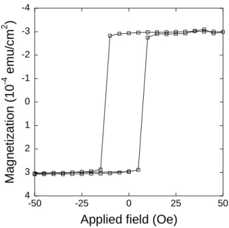
II.4.1.3. Determination of the hysteresis loop of the iron layer by electrical measurement ... 58
II.4.2. Spin-filter effect in the junction Pt / Co / MgO / n-Si ... 59
II.4.2.1. Transmission of unpolarized electrons ... 60
II.4.2.2 Transmission of spin-polarized electrons ... 61
II.4.3 Spin-valve effect in the junction Pt / IrMn / Co / Cu / Co / MgO / n-Si ... 62
II.4.3.1. Transmission of unpolarized electrons ... 62
II.4.3.2 Spin-dependent transmission of unpolarized electrons ... 63
II.4.4 What to conclude from the transmission experiments? ... 65
Chapter III
Optical detection of spin-filtering effects in ferromagnetic metal /
semiconductor junction ... 69
III.1. Ferromagnetic metal / semiconductor structure for cathodoluminescence ... 72
xi
III.1.2. Magnetic characterization... 74
III.1.3. Optical properties ... 76
III.1.4. Electron detection of electron injection and transmission in the InGaAs_1 junction ... 80
III.2. Cathodoluminescence experiments ... 83
III.2.1. The optical detection setup ... 83
III.2.2. Cathodoluminescence intensity versus injection energy ... 88
III.2.3. Spin asymmetry in the cathodoluminescence intensity and its asymmetry to the polarization of the incident beam ... 93
Conclusion and perspective ... 101
Appendix A: Details of samples introduced in the thesis ... 105
Appendix B: Details of data files introduced in the thesis ... 107
1
Introduction
In the early 1980’s, it was shown that inelastic electron scattering in ferromagnetic metals at energies well above the Fermi level depends on the orientation of the electron spin with respect to the magnetization [Unguris82, Kisker82, Hopster82, Penn85a]. This dependence is a direct consequence of the exchange interaction which induces a spin asymmetry in the electron density of states in the vicinity of the Fermi level. Different numbers of available empty states for the two directions of spin result in different values of the inelastic mean free path. Thus electrons which cross a magnetic thin film are spin-filtered. This effect was demonstrated in ballistic electron transmission experiments and the spin dependence of the electron inelastic mean free path was measured over an energy range which extends up to several tens of eV. [Pappas91, Getzlaff93, Schönhense93, Lassailly94, Vescovo95, Gröbli95, Drouhin96, Oberli98, Cacho02] This spin selectivity of ultrathin magnetic films has been exploited in magnetic domain imaging and in several model spintronic devices. [Monsma95, Filipe98, vanDijken03, Jiang04, Kinno97, Rippard99, Rippard00, Heer04, Kaidatzis08] Such devices, based on metal semiconductor junctions, exhibit high spin selectivity but suffer from high current attenuation. Attenuation can be compensated by increasing injection energy in order to benefit from secondary electron multiplication. [Filipe98, Rougemaille08] However, although the spin-dependent scattering is qualitatively well understood in the case of ballistic electron transmission, the situation is not so clear when dealing with inelastically scattered electrons.
The purpose of this thesis is to study the spin-dependent transport of electrons across ferromagnetic metal / semiconductor junctions as a function of the injection energy in a range which extends from 5 to 3000 eV above the Fermi level. Indeed, in high energy range the transport is dominated by electron-electron scattering which gives rise to the excitation of a secondary electron cascade. In this framework, several questions rise up like:
Introduction
2
1) How does spin-polarized electron transmission through the junction depend on the electron injection energy and on the metal / semiconductor barrier shape?
2) How to describe the energy and momentum relaxation which results in the formation of the secondary electron distribution?
3) Which spin transport processes have to be considered: relaxation, precession, filtering, dilution / exchange?
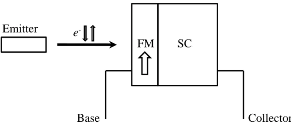
Figure A.1: Scheme of the three-terminal hybrid device. The emitter provides spin-polarized free electrons. The electrons are injected into the ferromagnetic metal (FM) / semiconductor (SC) junction. Base (metal) and collector (semiconductor) currents are separately detected.
In order to address these issues, we will have to answer the preliminary question of how to detect spin-dependent transport properties in a hybrid structure which combines ferromagnetic and semiconductor materials. The general scheme for such experiments is the one of a three terminal transistor-like device with a ferromagnetic metal base and a semiconductor collector. Then different configurations can be envisaged which mainly differ by the emitter. Our approach, schematized in Fig.I.1, is based on the use of a spin-polarized free electron source. The emitter is thus spatially separated from the base / collector junction, which offers the main advantage of controlling the spin polarization of the incident electron beam and that of accurately tuning the injection energy. The spin-polarized electron source is a p-doped GaAs
e
-FM
SC
Emitter
Introduction
3
photocathode activated in negative electron affinity. When excited in optical pumping conditions with circularly polarized near-bandgap light it produces an electron beam of polarization P0 = ± 25 %. The sign of P0 can be simply reversed by reversing the helicity of the
excitation light. The base, which contains one (or two) ultrathin ferromagnetic layer(s), acts as a spin filter by favoring the transmission of one electron spin state. It is required to exhibit a square hysteresis loop to achieve electron transmission in a persistent magnetic state. It is the relative orientation of the magnetization to the incident spin polarization, which determines the transmission of the base. Electrons travelling through the junction are detected at the collector as a transmitted current, whose magnitude depends on the magnetic state of the base. The other part of electrons, which are absorbed in the spin filter layer, contribute to the base current. Such transport measurements rely on the ability of independently measuring the base and the collector currents. This can only be achieved for junctions of very high impedance, provided by a Schottky-like barrier at the interface between the metal base and the semiconductor collector which exhibits a strong rectifying character. To work out a ferromagnetic metal / semiconductor junction with good rectifying behavior is a highly nontrivial task in practice. The main limitation comes from the fact that in a Schottky junction made of an abrupt metal / semiconductor contact, the interdiffusion between the metal and the semiconductor cannot be fully avoided. To overcome this problem we have explored two different approaches. One is to introduce a very thin oxide interfacial layer between the metal and the semiconductor which is known to improve the junction barrier and to prevent against the interdiffusion. The main difficulty is that the oxide layer has to be thin enough to let pass the electron without applying a bias. The other approach is to give up the electrical measurement of transmitted current and to develop instead an optical detection technique insensitive to the electrical properties of the junction. To do so we will exploit the light emitted from the recombination of the transmitted electrons into the semiconductor collector.
Introduction
4
experiments with emphasis on the energy range of electrons implicated in the transport. In Chapter 2, we present the first approach, where we study electron transmission through Metal / Insulator / Semiconductor junctions. Several structures are considered which differ one from the other by the composition of the metal layer, the thickness and bandgap of the oxide and finally by the semiconductor collector. In most samples we could not detect a reliable electron transmission signal at low injection energy (typically below few hundreds of eV) while, at high injection energy, we have obtained electron transmission larger than unity (because of secondary electron multiplication) and spin filtering effects. Finally, for samples containing two magnetic layers, no spin valve effect has been detected.
In Chapter 3, we describe the cathodoluminescence experiment that we have developed to exploit the radiative recombination of electron in the semiconductor collector in order to detect the transmission through the junction. For this purpose, specific semiconductor collectors have been grown with quantum wells to favor electron recombination close to the metal / semiconductor interface. We present the first results that we have obtained on the optical detection of spin-polarized electron transmission through ferromagnetic metal / semiconductor junctions.
In conclusion, we discuss the main limitations and advantages of the optical detection method and we present some perspectives for future experiments.
Chapter I
Spin-dependent effects
in magnetic thin films
Transport of electrons injected at energies well above the Fermi level
into empty bands is a complex problem. This chapter is intended to
present and discuss experimental results that are relevant to the
understanding of spin-dependent transmission experiments when
inelastic electron scattering dominates the transport properties.
Chapter I
Spin-dependent effects in magnetic substance
7
The present thesis work is related to the wide field of spintronics. Most of the approaches developed in this field concern the transport properties at the Fermi level EF. The giant
magnetoresistance (GMR) effect constitutes the most well-known paradigm. The approach pursued along this work deals with the transport of spin-polarized “hot” electrons having energies greater than EF. It makes use of tools at the frontier between electron transport and
electron spectroscopy techniques. We will briefly review the state of art in this domain, before describing the objectives of our work.
I.1 “Transport” at high energy in metallic thin films
The first energy range to consider is the low energy range of a few eV above EF (where
the electron transport through thin films is mainly ballistic). This situation is met in tunneling injection [Alvarado92, LaBella01, Vu11] and BEEM experiments [Rippard99, Kaidatzis08]. Electron transport above EF in the empty bands is ensured by thereafter called hot electrons,
which have the kinetic energy greater than EF and interact with the Fermi sea. Hot electron
transport can be described in term of mean free path as being the characteristic attenuation length, which is generally of the same order of magnitude as the thickness of metal layers.
Transport at higher energy range (several tens of eV) is far from being quantitatively well understood. Electrons crossing the sample interact with the conduction electrons, leading to the production of secondary electrons. The secondary emission is a cascade process of excitation from the Fermi sea combined with elastic and inelastic scatterings of the electron cascade. Thus a complete treatment of the secondary emission requires the knowledge of the electronic transition probabilities in the sample, of the scattering cross sections for elastic and inelastic electrons. So far, there is no single theory, which takes into account all of these features. However, previous results obtained in our group by the electron injection of energies up to 2 keV [Rougemaille08] will help us compare our spin dependence measurements of
Chapter I
8
electrons crossing ferromagnetic films.
Let us now give an overview of results, which are pertinent to the understanding of our work.
I.1.1 Low energy transport above EF in thin ferromagnetic films
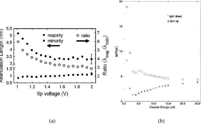
Figure 1.1: Hot electron transport. (a) Hot electron attenuation length for majority-spin and minority-spin electrons in Co in the energy range of 1 to 2 eV above the Fermi level, deduced from BEEM experiments [from Kaidatzis08]. Right: Inelastic mean free path calculated for majority-spin and minority-spin electrons in Fe at low energy [Hong00] (sp contributions are included). It evidences a large spin asymmetry in the mean free path (+ >> -) within about 10 eV from the vacuum level (electron energy equals zero). Its origin comes from the very strong spin-flip exchange scattering.
The key idea, common to all spin-injection experiments exploits the consequence of the imbalance of densities of the electronic states at EF in ferromagnetic metals: the inelastic
Spin-dependent effects in magnetic substance
9
mean free path of majority-spin electrons is larger than that of minority-spin electrons in an energy range up to 50 eV above EF [Penn85b, Pappas91, Grobli95, Oberli98, Weber01]. In
other words the scattering rate for minority-spin electrons injected into the ferromagnetic empty band is enhanced due to the excess of minority spin holes. (cf. Figure 1.1)
This asymmetrical transport of spin-polarized electrons gives rise to electron spin filtering in thin ferromagnetic films. The spin filtering techniques may be loosely classified into three groups.
1) Spin filter
Figure 1.2-a illustrates how to operate a spin filter. When an electron beam of spin polarization P0 strikes an ultrathin ferromagnetic sample the transmitted current depends on
the relative orientation of the incident spin polarization with respect to the film saturated magnetization.
One of the properties of the spin filter is that its spin selectivity depends on the energy of hot electrons traveling through the ferromagnetic film. The spin filter is characterized by the following experimental quantities:
- The asymmetry A of the transmitted current A = ( I+ - I-) / ( I+ + I- ), I+ ( I- ) being the transmitted current for +P0 (-P0) respectively;
- The spin-dependent transmission T = ( I+ - I- ) / I0, I0 being the incident current;
- And by analogy to spin polarimetry, its capability of spin discrimination, the so-called Sherman function S. It is the polarization acquired by an unpolarized beam when passed through the spin filter.
Chapter I
10
Figure 1.2: Working principle of spin filter in transmission geometry. (a) The ultrathin magnetic film preferentially transmits electron whose incident spin direction is parallel to the magnetization orientation. One of the prerequisites for having a spin filter relies on the square hysteresis loop with two saturated magnetized states +M and –M. Thus electron transport occurs under zero applied magnetic field. Reversing the saturated magnetization from +M to –M is equivalent to switching the incident electron polarization from +P0 to –P0. For a given magnetization an asymmetry between the
transmitted currents I + and I - is measured. (b) Experimental results showing the spin-filter effect in the Fe / GaAs junction. Variation of the transmitted current IC as a function of time, when modulating
periodically the polarization of the incident electrons between +P0 and –P0. When flipping the
magnetization the spin filtering effect is reversed. <IC> refers to the spin-independent part of the
transmitted current IC. The current scale is in nA.[Rougemaille03]
Typically the structure Au / Co / Au (1 nm thick Co layer) has a transmission of 4 × 10⁻⁴, a spin-dependent transmission T = 6 × 10⁻⁵ and a current asymmetry A = 8.5 % for an incident electron polarization of 25 %. The Sherman function value of such a spin filter is 0.34 for low injection energy, less than 5 eV. It can be shown that the transmission asymmetry verifies the equation A = P0 S. It means that to measure a spin-dependent asymmetry an initial
spin polarization P0 is required in conjunction with the spin-filter layer. This is the working
e- FM M H +P0 +M -M -1.5 -1 -0.5 0 0.5 1 1.5 0 2 4 6 8 10 0 2 4 6 8 10 +M -M time (ms) time (ms) IC ( ) -< IC > +P0 -P0 +P0 -P0 -P0 I+ I -(a) (b)
Spin-dependent effects in magnetic substance
11
condition of a spin filter.
Two experimental configurations have been explored for measuring spin filter effect: either the transmission takes place through a freestanding foil, such as Au / Co / Au of total thickness of 21 nm [Lassailly94, Oberli98] or through a compact structure, where the ferromagnetic layer is deposited on a bulk semiconductor, the latter collecting the transmitted current [Filippe98, Rougemaille03]. It is the latter configuration that we will use in the thesis.
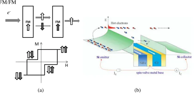
2) Spin valve: polarizer-analyzer experiments [Mousma95, Jansen01, Rippard00, Cacho02, VanDijken03]
Figure 1.3: Working principle of spin-valve device. (a) An unpolarized electron beam is transmitted through two uncoupled ferromagnetic layers separated by a nonmagnetic layer. The two magnetic layers act as polarizer and analyzer of electron spins, such that the relative orientation of the magnetization of the two layers determines the transmission of the base. (b): Schematic energy diagram of a spin valve transistor. Hot electrons are injected above the Fermi level. Hereby the incident electron energy is determined by the height of the Schottky barrier between the semiconductor emitter source and the metal base [from Jansen03].
e -FM FM M H FM/FM (a) (b)
Chapter I
12
The spin filtering effect can be exploited for achieving the optical equivalence of the polarizer-analyzer combination. Two ferromagnetic layers are required (Figure 1.3), the first one selecting a population of spin-polarized electrons, the second one detecting the projected spin component along the magnetization direction. The resulting salient feature is that the collector current depends on the magnetic state of the spin-valve layers, i.e. the base. Examples of spin-valve device include the magnetic tunneling transistor and the spin-valve transistor. Both devices are junctions sensible to electronic properties of interface, the transmission probability being determined by energy and momentum constraints imposed by the band structure difference between the semiconductor and the metal interface. Such junctions operate in low energy range from 0.8 to 2 eV, higher voltages resulting in a breakdown of the junction. To explore a higher energy range the electron source has to be decoupled from the spin-valve structure. It is the strategy that we have followed during this work. It also offers the advantage of optically controlling the incident spin polarization and tuning the energy of incident electrons up to 3 keV.
3) Spin-precession of the polarization
When the spin-polarization vector of the incident electron beam is perpendicular to the magnetization of the ferromagnetic layer, then it rotates into the direction of the magnetization and simultaneously precesses around it. The angle of rotation depends on the spin asymmetry
A [Oberli98]. The rotation around the magnetization is the optical analog of the linear
magneto-optics Faraday effect, the light propagation vector being oriented along the magnetization vector. Precession of electron spin can also be generated by the reflection at ferromagnetic surface [Weber02], by the injection of spin-polarized beam into non-magnetic materials but under a continuous magnetic field [Huang07]. Typically electron energy involved in spin-precession experiments is in the range of a few eV.
Spin-dependent effects in magnetic substance
13
Figure 1.4: Spin-precession effect. When electrons are injected into the ferromagnetic layer with the spin direction normal to the magnetization, the electron spin will rotate of the angle α into the direction of the magnetization of the layer and at the same time process around it.
I.1.2 High energy transport: the secondary electrons at play
Electron transmission in spin-valve structure up to 100 eV of injection energy reveals a linear increase versus the injection energy due to the secondary electron multiplication [Cacho02]. As soon as electrons enter the metal cap layer prior the magnetic filter, the secondary electron process induces a dilution of the initial spin polarization. Consequently the polarization of secondary electrons does not depend on the polarization of the injected electrons. At very high injection energy up to 3 keV, we can only predict an increase in the electron mean free path by referring to the well-known E1/2 variation of the electron mean free path versus electron energy. The ballistic transport is no longer valid in all sample thickness and must be replaced by the spatial evolution of a distribution composed of primary electrons, which keep the memory of the initial spin polarization, and secondary electrons. Varying the incident energy amounts to broad the electron distribution reaching the interface metal / semiconductor. The electron energy distribution of secondary electrons is characterized by a mean energy εM, which corresponds to the energy of electron travelling
within the interface and an amplitude given by the secondary multiplication factor. The collected current corresponds to the upper energy part of the electron distribution, the lower
e
-FM
Chapter I
14
part being successively energy filtered when crossing interface barriers. The spin-dependent part of transmission in the spin filter can be included by considering two electron distributions for the primary electrons, each being associated with spin-dependent mean free paths + and
-. Figure 1-.5 gives a pictorial representation of the different transport mechanisms involved in the spin filter.
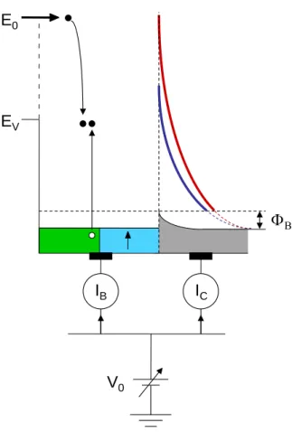
Figure 1.5: Schematic layout showing the transport in the structure metal / semiconductor based on the electron-electron interaction, each scattering yielding two electrons. B is the Schottky height, EV
the vacuum level and E0 the energy of incident electrons. The incoming electron relaxes its energy in
the metal base by generating a cascade of secondary electrons. The base current IB corresponds to
electrons, which have not enough energy to surmount the barrier B. Electrons which pass the barrier
form the collector current IC in the semiconductor. The spin filter effect results in two different energy
distributions of the transmitted electrons (red and blue curves), whose low energy part is cut off by the barrier B. The currentIC is actually the integral in energy of the energy distribution. The potential V0
applied on the two terminals of the junction determines the injection energy E0. B
EV E0
IB IC
Spin-dependent effects in magnetic substance
15
Increasing the incident energy E0 amounts to a boost in the multiplication of secondary
electrons, and therefore to a broadening of the electron distribution resulting from the subsequent cascade. The unknown quantity, which is not directly accessible from our measurement, is the mean energy εM of the electron distribution within the sample. Its
variation with the injection energy E0 can be obtained by self-consistently solving the
equation which yields the total transmission T through the junction:
where the value of αSC (αOx) the collection efficiency in the semiconductor (the oxide layer),
and ΦSC (ΦOx) the semiconductor band bending barrier (the oxide layer barrier height) are
known [Rougemaille08]. The exponential function reproduces the accumulation of secondary electrons due to the electron cascade. Figure 1.6 shows the variation of εM versus E0 deduced
from the experimental measurement of the transmission through the Fe / Oxide / GaAs sample.
Figure 1.6 [Rougemaiile08]: Calculated variation of the electron mean energy εM, which describes the
electron distribution width at the metal / Oxide interface in the structure Fe (3.5 nm) / Oxide / GaAs as a function of the injection energy E0. Horizontal dotted lines correspond to the two barrier heights ΦOx
and ΦSC. 3 1 0.3 10 100 1000 E0(eV) εM (eV) ΦOx= 4.5 eV ΦSC= 0.78 eV
Chapter I
16
I.2 Our experimental strategy
We briefly list the main features, which constitute the backbone of our experimental work. They will be thoroughly described in the next chapters.
I.2.1 A three-terminal device or the importance of having an abrupt, high-quality Schottky barrier
The metal base, which includes the spin-filter layer, is grown on the semiconductor substrate, which is used as a collector. The spin injection is achieved by an electron source separated from the base-collector electrodes by vacuum. The two electrodes are connected to the same potential, which defines the injection energy. The potential barrier formed at the metal-semiconductor interface has to fulfill two objectives. First, as previously mentioned, it ensures the selectivity in energy of the transmitted electrons. Electrons of energy below the potential barrier are collected in the base layer. Second, the barrier provides a junction resistance, whose value should be high enough for measuring independently the base current and the collector current under zero applied voltage to the junction. We will have to find out how to accurately measure the junction resistance.
I.2.2 What type of metal-semiconductor junctions?
Effort has been concentrated in our group on the growth of Fe on GaAs [Filippe98] to form a Fe / GaAs Schottky diode. The electrical properties of such samples are given by quality of the metal / semiconductor interface. Indeed the junction must block electrons of energies below the barrier. Pin holes and defects at the interface give rise to leak currents, which can compensate the current passing over the barrier. Also our working conditions
Spin-dependent effects in magnetic substance
17
require using samples of quite large area (typically 7 × 7 mm2). To overcome these obstacles, the approach is to form a Schottky-like junction. In this type of structure, a very thin oxide layer of different thicknesses (typically from 1 to 3 nm) is grown at the interface between the metal and the semiconductor.
In a first step we will study the archetype junction Pd / Fe / oxide / n+ - GaAs, whose spin-polarized-electron transport has been experimentally and theoretically analyzed [Rougemaille08, Lamine07]. The structure contains a single iron layer grown onto a 2 nm thick oxide layer. Then in a second step transmission through junctions having different thicknesses of oxide will be compared with transmission through the Pd / Fe / oxide / n+ - GaAs. These junctions are fabricated by our collaborators of the group “Nanomagnetism and Spin-Electronics”, led by Michel Hehn, at the Laboratory of Material Physics of Nancy University.
I.2.3 What type of detection for the transmitted electrons?
As early described in the chapter, the principle of all injection experiments is based on the electrical measurement of currents transmitted through the sample. The price to pay is the necessity of working with a high impedance sample. Indeed such a measurement amounts to detecting a weak current flowing through finite impedance terminals. In particular it remains to determine the threshold of detection for the transmitted currents. Another alternative to the current measurement is the optical detection of the transmitted current. Based on the formal analogy between polarizing and analyzing spin filter, one might expect that GaAs is not only a source but also a detector of spin polarization. This means to carry out a cathodoluminescence experiment, in which the transmitted electrons recombine with holes across the semiconductor band gap thereby by emitting light. Moreover spin-polarized electrons should produce circularly polarized luminescence. The oxide barrier presented in the previous samples is now
Chapter I
18
replaced by the energy gap of semiconductor. A new junction comprising the electron-photon converter part has been elaborated by Oleg Tereschenko of the Institute of Semiconductor Physics in Novosibirsk. The main advantage of the optical detection is that the constraint of having a rectifying behavior is now avoided. A new experimental setup will be developed to meet the need of such luminescence detection.
Chapter II
Electrical detection of spin-filter effect in
ferromagnetic metal / semiconductor
junctions
The existence and the properties of spin-filtering in ferromagnetic
metal / semiconductor rectifying junctions can be measured by injecting
spin-polarized electrons into empty bands of the ferromagnetic metal. In
this chapter we review the experimental configuration to achieve such a
transport measurement. Then we present the transmission results
obtained from junctions having one or two ferromagnetic layers. We also
show the effect of an interfacial oxide barrier introduced between the
metal and the semiconductor.
Chapter II
Electrical detections of spin-filter effect in the ferromagnetic metal / semiconductor junctions
21
II.1
The objectives
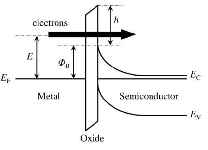
Our experimental approach relies on injecting spin-polarized electrons into a ferromagnetic metal / oxide / semiconductor (hereafter referred as MIS) junction, where the oxide layer behaves as a tunnel potential barrier for electrons having an energy less than the barrier height (E < ΦB + h, Figure 2.1).
Figure 2.1: Schematic energy diagram of electrical injection and detection at zero bias in MIS junction with n-type semiconductor substrate. ΦB is the Schottky barrier height (i.e. the barrier height
due to the semiconductor band bending). The main issue discussed in this chapter revolves around the oxide thickness, which affects the I-V characteristics and the results of the transmission experiments. E is the injection energy referred to the Fermi level EF.
The junction has to fulfill the following criteria.
The electrical properties. When collecting current on a metal electrode in ultra-high vacuum environment, the current flows through an infinite impedance, which is the impedance of the vacuum / electrode barrier. This is the ideal configuration to measure small currents, when, for instance, performing direct electron transmission through a freestanding sample [Cacho00]. However, measuring the current crossing a junction turns out to be limited
Metal Semiconductor h EF EC EV ΦB electrons E Oxide
Chapter II
22
by the intrinsic resistance of the junction, as it will be explained in § III.3.4. Therefore the equivalent resistance of the junction has to be as large as possible. In principle, when injecting high energy electrons into a junction, the rectifying character of the metal / semiconductor contact should provide high enough junction impedance to allow independent measurement of the currents flowing in the metal and in the semiconductor terminals. In practice, this is often not the case. Then, inserting an oxide layer (which introduces a barrier for both charge transport and atoms interdiffusion) between the ferromagnetic metal and the semiconductor provides a means of controlling the junction resistance. The oxide layer must be thin enough to behave as a tunnel barrier (Figure 2.1).
The magnetic properties. In our experimental geometry, the samples must contain ferromagnetic layers with in-plane magnetic anisotropy so that the spin polarization of the incident electron beam is parallel to the sample surface. We recall that our concern is to measure the transmitted current according to the relative orientation between the spin polarization and the saturated magnetization of the ferromagnetic layers. The number of ferromagnetic layers allows one to investigate either the spin-filter effect (one ferromagnetic layer) or the spin-valve effect (two ferromagnetic layers). In the case of the spin-valve sample the coercivity of each ferromagnetic layer should be quite distinct in order to reverse the magnetization of one layer without affecting the second one.
Thickness consideration. Concerning the interfacial oxide layer, it must be thin enough (in the range of 1~3 nm) to differ from the genuine metal / insulator / semiconductor capacitor. Concerning the metal layer thickness, as shown by the previous transmission experiments [Rougemaille03, Lamine07, Rougemaille08], the overall metal multilayer film has to be less than 20 nm thick, otherwise the transmission factor becomes too weak to give a detectable transmitted current.
Electrical detections of spin-filter effect in the ferromagnetic metal / semiconductor junctions
23
II.2
Nature of junctions
II.2.1 Sample structures
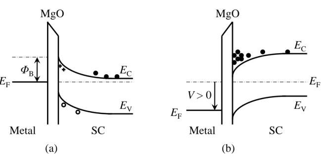
Figure 2.2: Schematic diagram of MgO interface in the junction Co / MgO / Si. (a) Zoom of the interface Si(100) / MgO(100) showing a highly textured MgO layer of 2 nm and a sharp and atomically flat interface [Bernos10]. An amorphous Si layer is between the Si substrate and the MgO layer. (b) Energy-band diagram of an ideal metal / MgO / semiconductor junction (equal metal and Si work function ΦS). The gap of MgO EGi = 7.6 eV, the electron barrier height ΦBe = 3.7 eV, the hole
barrier height ΦBh = 3.0 eV, the energy gap of Si is 1.1 eV, and the electron affinity of MgO
χM = 1.5 eV. [Parkin04, Kurt10]
As previously stated, an oxide layer is grown on the semiconductor substrate prior to the deposition of the ferromagnetic layer. We have used three types of oxide layers: magnesium oxide (MgO), aluminum oxide (Al2O3) and gallium oxide (Ga2O3) generated at room
temperature by UVOCS (“Ultra-Violet Ozone Cleaning System”). However, the samples
ΦBe
ΦBh
Metal MgO Semiconductor
EF EF EC EV EGi ΦS χM Vacuum level (a) (b)
Chapter II
24
containing a 2 nm thick aluminum oxide barrier show no photogenerated current under the light illumination (the main reason for that will be further described). In the rest of the thesis we will confine ourselves to the junctions with the two other types of oxides. All the semiconductors substrates are n-doped, so the majority carriers are electrons.
1. The junction Pd (5 nm) / Fe (4 nm) / Uvocs (10 Å) / n-GaAs, hereafter referred to as GaAs_1, which is the “canonical” junction, has been successfully studied in our group [Rougemaille03, Lamine07, Rougemaille08]. It will be used as the reference sample to give evidence to the effects due to the nature of barrier in the transmission experiments.
2. The junction Pt (3 nm) / Co (5 nm) / MgO (100) (2 nm) / n-Si (100), hereafter referred as MgO_1, to study the spin-dependent electron transport in Si. The choice of the MgO barrier is dictated by a barrier height higher (3.7 eV for an ideal MgO tunnel barrier, assuming that the Fermi level is pinned mid-gap, i.e. in the absence of fixed oxide charges, see Fig.2.2-b) than the amorphous Al2O3 barrier of 2.6 eV and by a
higher magnetoresistance in the magnetic tunnel junctions. According to the deposition process worked out by Bernos et al in Nancy [Bernos10], the MgO layer, which is RF sputtered on a unoxided silicon surface is textured with a very good planarity. The Figure 2.2-a shows the high-resolution cross-section image of the sample after annealing obtained by transmission electron microscope: starting from the Si (100) substrate, an amorphous Si layer followed by the 2 nm thick barrier can be successively observed.
3. The bilayer structure Pt (2 nm) / IrMn (7.5 nm) / Co (5 nm) / Cu (3.5 nm) / Co (5 nm) / MgO (3 nm) / n-Si (100), denoted by MgO_2. It contains two ferromagnetic layers decoupled by a thin non-magnetic Cu metallic layer. One of the cobalt layers is covered by the antiferromagnetic layer IrMn, which shifts the cobalt hysteresis loop due to the exchange interaction at the interface of both layers. To crystallize the MgO
Electrical detections of spin-filter effect in the ferromagnetic metal / semiconductor junctions
25
junction and to block the exchange layer, the structure has been annealed for 1 hour in an external field of 200 Oe directed along its easy axis. This structure is designed to form a spin valve for hot electrons. The first cobalt layer polarizes the electron beam by passing a spin direction. The second cobalt layer stops or transmits the polarized electrons depending on its magnetization orientation with respect to the one of the polarizing layer.
The two last samples were grown at the Laboratory of Material Physics (LPM), at the Nancy University.
II.2.2 Electric characterization of the samples
II.2.2.1 Current transport in metal / oxide / semiconductor structures
As previously mentioned, all the samples dedicated to the electron transmission experiments should present the rectifier electrical properties, so that the junction resistance is much larger than the access resistance of the junction. Here we start to give a short survey of the electronic transport in metal / insulator / semiconductor structure.
In MIS structure, the current-voltage characteristics critically depend on the insulator thickness, since the tunneling probability varies exponentially with the thickness. If the insulator layer is sufficiently thick (for instance, for the Si-SiO2 system greater than 7 nm
[Av-Ron78]) the carrier transport through the insulator layer is negligible and the MIS structure is equivalent to a conventional MIS capacitor. On the other hand, if the insulator layer is very thin (less than 1 nm), little hindrance is met by carriers flowing between the metal and the semiconductor, and the electric behavior looks like a Schottky-barrier diode at least at low bias voltages. Then most of the biasing voltage will be applied to the semiconductor. In this case, the tunneling probability term exp(- d h1/2), where d is the oxide
Chapter II
26
thickness and h is the mean barrier height (Figure 2.1), is close to unity and the tunneling current can be approximated by an expression similar to the standard thermionic-emission equation for Schottky barriers. Samples having an ultra-thin oxide layer (≤ 2 nm) should correspond to the latter case. The basic transport mechanisms are the thermionic emission and tunneling. The tunneling current dominates when the width of the depletion layer is thin enough. Here we recall that the depletion-layer width decreases with the impurity concentration of the semiconductor. So for heavily doped semiconductors the tunneling current may become more significant. The major expected differences of MIS structure compared to the conventional metal / semiconductor contact should be a reduced thermionic current of electrons because of the additional interfacial layer without affecting the minority current, a lower barrier height (the existence of defect states across the interfacial layer), a higher ideality factor, and the possibility of modulating the carrier concentration at the semiconductor surface by bias voltages (then all the applied voltage drops across the oxide barrier). Along this thesis, by ease of use we will designate our samples as Schottky-barrier diodes.
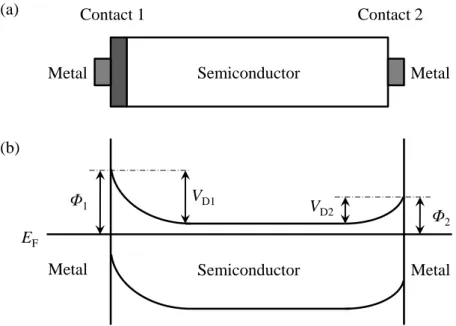
When measuring the I-V characteristics of Schottky-barrier samples, some specific care has to be taken because of recurrent high contact resistances. Figure 2.3 shows such a case, where the back side contact has a high contact resistance. The two-terminal device essentially corresponds to two metal / semiconductor contacts connected back to back, i.e. two Schottky barriers connected back to back. When a low negative voltage is applied to the metal-semiconductor contact 1 with respect to Contact 2, the barrier Φ1 is reverse-biased and
Φ2 is forward-biased. The applied voltage is shared between these two contacts but most of
the voltage drop will occur across the depletion region of Contact 1. The electron current is due to the thermionic emission of electrons from Contact 1. Note that the current continuity requires that the reverse current for the Contact 1 is equal to the forward current for the Contact 2, assuming same areas for both contacts. Therefore to avoid the voltage drop across
Electrical detections of spin-filter effect in the ferromagnetic metal / semiconductor junctions
27
the barrier of the Contact 2, we need to have an Ohmic contact with a very small contact resistance compared to the semiconductor resistance. A criterion to check the nature of transport across the back side is to measure the current-tension (I-V) characteristics under light illumination of energy larger than the semiconductor energy band gap. Indeed electrons, which are photoexcited across the semiconductor energy band gap, will diffuse toward the back side of junction in the same direction as the reverse saturation current, which gives an augmented current. The absence of such a photocurrent in I-V curves under reverse bias means that most of the carriers are blocked by a Schottky barrier on the back side. We will now briefly describe the I-V characteristics of an ideal Schottky diode, which we will use to analyze the rectifying electrical properties of our samples.
Figure 2.3: Schematic diagram of (a) a two-terminal device constituted of a Metal / Oxide / n-doped Semiconductor structure with the metallic contacts on both sides, whose high contact resistance at the back side (Contact 2) leads to two Schottky barriers connected back to back (the oxide layer is not shown), and (b) the corresponding band energy diagram at thermal equilibrium, where 1 and 2 are
the barrier heights for electrons and VD1 and VD2 are the built-in potentials for contacts 1 and 2
respectively [Tantraporn70]. Semiconductor Metal Metal Contact 1 Contact 2 EF VD1 VD2 Φ1 Φ2 (a) (b)
Chapter II
28
Figure 2.4: (a) Energy band diagram of metal on n-type semiconductor under different biasing conditions V. The electron flow is more important under Forward bias (V > 0) than under Reverse bias (V < 0). And (b) its equivalent circuit including the (access) series resistance RS and the differential
resistance RP including the resistance due to the Schottky barrier and the resistance due to leak current
through the junction. The differential capacitance of the space charge region is omitted. In the electron transmission experiments, the resistance RS will be assimilated to the contact resistance rB.
(cf. Figure 2.20)
In the assumption of an ideal Schottky diode with moderately doped semiconductor, the main transport mechanism is the thermionic emission of majority carriers from the semiconductor over the potential barrier B into the metal. The current density flowing in the
junction under an applied voltage V is given by the well-known equation:
J = J0 [exp (eV / kT) – 1], where J0 = A* T 2 exp (-B / kT) is the saturation current density
[Rhoderick78]. The effective Richardson constant A* is equal to 8.64 A·cm-2·K-2 for GaAs, 246 A·cm-2·K-2 for silicon in (100) directions, and 258 A·cm-2·K-2 for silicon in (111) directions, respectively. The equivalent circuit of a Shottky barrier includes the series resistance RS which accounts for the contact resistance and the resistance of the neutral
RP RS Metal Semiconductor EF EC EV EF V Metal Semiconductor EF EC EV EF V Forward Reverse (a) (b)
Electrical detections of spin-filter effect in the ferromagnetic metal / semiconductor junctions
29
semiconductor region between the ohmic contact and the depletion region (Figure 2.4). Therefore the voltage drop across RS causes the actual voltage drop across the depletion
region to be less than the applied bias V. So in the above equation, the applied bias V has to be replaced by the effective bias Veff = V – IRS, I being the current through the diode, which
stands for the real potential drop across the barrier.
The following parameters fully characterize the electrical performances of our Schottky diodes:
- J0, the dominant electron flow from the metal to the semiconductor for low reverse bias V.
We thereafter refer to reverse bias as positive voltage applied to the n-type semiconductor back side with respect to the metal side. For small V values, J J0 eV / kT, and 1 mV bias
gives a current density J J0 / 25, which constitutes the lower limit of the polarization
current. Therefore since our transmission experiments will be performed at zero bias, the samples must have values of J0 as low as possible. The additional argument for minimizing
J0 is that the mean square noise current of shot noise for the Schottky junction is
proportional to J0. We will show that values of dark current of a few nA can be strongly
detrimental for the detection of transmitted current. - B, the potential barrier.
- The ideality factor n = e / kT [dV / d(ln J)], whose deviation from unity indicates that the thermionic transport is not the only dominant mechanism.
- The dynamic resistance of the Schottky barrier R0 = S -1
(dJ / dV)-1 = kT / [ e S (J + J0)]
measured at zero bias (S is the surface of the sample), arising from the space charge region, where electrons are depleted in n-type semiconductor. Note that for several tenths of a volt of reverse bias J ≈ – J0 and R0 becomes infinite. The R0 resistance determines the Johnson
Chapter II
30
II.2.2.2 How to measure I-V characteristics
Figure 2.5: Three-terminal I-V measurement. (a) Experimental setup. The voltage is applied across the back terminal, I is the measured current through the MIS structure and Veff corresponds to the genuine
voltage applied to the back contact. Since the voltmeter has very high impedance, the current flowing between the back side pads is practically zero. (b) Equivalent circuit. D and D’ correspond to the back junction and the front junction respectively.
We perform all the measurements with three-terminal system to directly get the real applied voltage Veff to the back side of the sample, as shown in Figure 2.5.
To form an ohmic contact on the semiconductor backside, we deposit a drop of liquid metal, a gallium based alloy. The bias voltage Vapp is applied to one pad on the back side and
the voltage effectively applied Veff is measured on the other pad. Then the voltage difference
Vapp – Veff corresponds to the voltage drop across the back side contact due to contact
resistances and local junction resistance of non perfect ohmic contact. Two voltage followers are used to provide enough current gain. A soft gold tip is gently pressed on the top metal surface of the sample to measure the total current I, which is then converted into the output
+ -+ -+ -Laser Sample Rf=1kΩ Rout=100Ω I Vout Vapp Veff Vapp Veff I Back Front D’ D (a) (b)
Electrical detections of spin-filter effect in the ferromagnetic metal / semiconductor junctions
31
voltage Vout of the amplifier with respect to the ground. Another gold tip is used to
mechanically hold the sample. The I-V measurements can be easily performed in the dark and under illumination (630nm, 1.4mW).
In this configuration, the voltage is applied to the semiconductor side of the sample, which is opposite to the convention generally used in the measurement of I-V. Thus, in order to simplify the analysis of the electrical measurements and avoid any ambiguities, our I-V curves will be drawn to be compatible with the usual configuration, where the voltage is applied to the metal side of the diode.
II.2.2.3 Electrical characterizations of the samples
II.2.2.3.a Pd (5 nm) / Fe (4 nm) / Uvocs (1 nm) / n-GaAs, (sample GaAs_1): An excellent Schottky diode
For simplicity, bias denotes the real voltage applied to the junction of the sample Veff. The
I-V curves (Figure 2.6) present the electrical characteristics of a Schottky-barrier diode. A forward bias (positive voltage applied to the metal) decreases the potential barrier for electrons moving from the semiconductor into the metal. As the bias increases the current densities measured in the dark and under illumination follow an identical increase. On the other hand, in the reverse direction, a nearly constant difference of 1875 μA/cm2 between the two measured densities appears as the negative bias increases. It leads to a photovoltage of 0.24 V, which corresponds to the positive shift of the minimum of the absolute current density. The existence of a photocurrent demonstrates that electrons generated in the conduction band of the semiconductor diffuse toward the metal contact on the back side, while holes created in the valence band diffuse toward the front metal contact. Let us emphasize that this photocurrent can be collected without bias.
![Figure 1.6 [Rougemaiile08]: Calculated variation of the electron mean energy ε M , which describes the](https://thumb-eu.123doks.com/thumbv2/123doknet/2924367.76742/32.892.308.637.667.982/figure-rougemaiile-calculated-variation-electron-mean-energy-describes.webp)