Pépite | Croissance et transfert de graphène et nitrure de bore hexagonal : applications thermiques pour l'électronique flexible
97
0
0
Texte intégral
(2) Thèse de Théo Levert, Université de Lille, 2019. 1 © 2019 Tous droits réservés.. lilliad.univ-lille.fr.
(3) Thèse de Théo Levert, Université de Lille, 2019. Remerciements. Je ne peux terminer ces trois années et demi de thèse, riches en découvertes et émotions sans procéder à quelques remerciements. Cette thèse s’est déroulée entre l’IEMN à Lille et CINTRA à Singapour, sous la direction de Henri Happy et Philippe Coquet et sous l’encadrement de Emiliano Pallecchi et Edwin Teo Hang Tong. Je tiens tout d’abord à les remercier chaleureusement pour leur accueil, leurs conseils, leur expertise mais aussi leur relation avec moi durant les différents séjours effectués à Lille ou à Singapour, et de m’avoir offert d’excellentes conditions pour la réalisation de mes travaux. Je tiens aussi à remercier les membres de mon jury, à savoir Mme la Présidente Christelle Aupetit-Berthelemot de l’université de Limoges, les rapporteurs Aziz BenlarbiDelai de Sorbonne université et Laurent Pichon de l’université de Rennes, ainsi que Bérengère Lebental de l’université Paris Est, examinatrice. Ils ont su lire mon travail, le juger et me questionner pertinemment sur ces travaux. Je tiens aussi à remercier les personnes avec qui j’ai pu collaborer durant ces travaux, à savoir les membres de l’équipe techno, notamment Elisabeth Galopin, Pascal Tilmant, François Vaurette et tous les autres pour leurs conseils sur les différentes étapes technologiques. Un remerciement tout particulier à Dominique Vignaud avec qui j’ai pu travailler étroitement sur l’aspect matériau et son aide pour la spectroscopie Raman. Je remercie aussi Tous les autres membres de l’équipe CARBON avec qui j’ai pu travailler, à savoir Emmanuelle Pichonat, Wei Wei, Soukaina Bensalk et Dalal Fadil. Un gros merci aux personnes de l’équipe CINTRA qui m’ont épaulé et permis de m’intégrer facilement dans la vie du laboratoire et plus généralement dans la vie singapourienne, à savoir Ange, Nicolas, Mathieu, Etienne, Holger et les autres. Un gros merci, comme le dit Charles Aznavour à « mes amis, mes amours, mes emmerdes », qui seraient un peu trop long à citer ici. Je remercie quand même toute la team Picardie, avec qui nos liens d’amitiés perdurent dans le temps, ainsi que mes nouveaux amis lillois. Je tiens tout particulièrement à remercier le Uno’s bar pour m’avoir permis de décompresser les nombreux soirs où c’était nécessaire, autour d’une bière et d’une partie de Ping-Pong, m’ayant permis de faire des rencontres incroyables. 2 © 2019 Tous droits réservés.. lilliad.univ-lille.fr.
(4) Thèse de Théo Levert, Université de Lille, 2019. Je tiens à remercier aussi mes colocs incroyables Pilou, Léo et Jordane qui m’auront permis durant cette quasi dernière année de retrouver un chez nous, non pas désert comme le dit Aznavour, mais rempli de vie et d’amour, au rythme des barbecues et soirées musiques. Enfin je tiens à remercier mes parents et ma famille qui m’auront soutenu (et surtout supporté) durant ces années.. 3 © 2019 Tous droits réservés.. lilliad.univ-lille.fr.
(5) Thèse de Théo Levert, Université de Lille, 2019. Table of content. Remerciements ...................................................................................................................... 2 General Introduction ............................................................................................................. 6 Chapter 1: Growth, transfer and characterization of graphene and h-BN ........................... 8 I). Introduction ............................................................................................................... 8 I.1). Objectives ............................................................................................................ 8. I.2). Graphene ............................................................................................................. 9. I.3). h-BN ................................................................................................................... 12. II). Growth and transfer of 2D graphene ...................................................................... 16 1). CVD growth of graphene ................................................................................... 16. 2). Characterization of graphene............................................................................ 19 a). Optical microscopy ........................................................................................ 20. b). Scanning Electron Microscopy ....................................................................... 21. c). Raman spectroscopy...................................................................................... 22. 3). Growth of 2D polycrystalline graphene ............................................................ 25. 4). Characterization of the grown graphene .......................................................... 27. 5). Transfer of 2D graphene ................................................................................... 29. 6) III). a). Method of transfer ........................................................................................ 29. b). Characterization of transferred graphene..................................................... 31 Growth of 2D monocrystalline graphene .......................................................... 35. Growth of 3D graphene ........................................................................................... 38 1). Growth of graphene on Nickel foam ................................................................. 38. 2). Characterization of the Foam ............................................................................ 40. IV) Growth of 2D h-BN .................................................................................................. 41 1). CVD growth of h-BN .......................................................................................... 41. 2). Growth of 2D polycrystalline h-BN.................................................................... 43. 3). Characterization of the grown h-BN ................................................................. 44 4. © 2019 Tous droits réservés.. lilliad.univ-lille.fr.
(6) Thèse de Théo Levert, Université de Lille, 2019. 4). V). Transfer and characterization of h-BN .............................................................. 50 a). Method of transfer ........................................................................................ 50. b). Characterization............................................................................................. 53. Growth of 3D h-BN .................................................................................................. 55 1). Growth of h-BN on Nickel foam ........................................................................ 55. 2). Characterization of the foam ............................................................................ 55. VI) Conclusion................................................................................................................ 56 Chapter 2: 3DC and 3DBN foam infused with polyimide .................................................... 57 I). Introduction ............................................................................................................. 57. II). Infusion of 3D foam with polyimide ........................................................................ 58 1). First generation of substrate ............................................................................. 58. 2). Second generation of substrate ........................................................................ 60. III). Characterization of the substrates .......................................................................... 61 1). Mechanical properties....................................................................................... 61. 2). Electrical properties .......................................................................................... 65. 3). Thermal properties ............................................................................................ 67. 4). a). First generation of substrates........................................................................ 70. b). Second generation of substrates ................................................................... 74 Dielectric constant measurement ..................................................................... 75. IV) Conclusion................................................................................................................ 77 General conclusion .............................................................................................................. 78 List of abbreviations ............................................................................................................ 79 References ........................................................................................................................... 80 Scientific publications .......................................................................................................... 88 Annex ................................................................................................................................... 89 I.. Growth and transfer of graphene and h-BN............................................................ 89. II.. Printed transistors ................................................................................................... 90. III.. Organization on the time passed on each lab ......................................................... 96. 5 © 2019 Tous droits réservés.. lilliad.univ-lille.fr.
(7) Thèse de Théo Levert, Université de Lille, 2019. General Introduction. General Introduction As the fourth most abundant element in the universe, Carbon plays an important role in the emerging of life in earth as we know it today. The industrial era has seen this element at the heart of technological applications due to the different ways in which carbon forms chemical bonds, giving rise to a series of allotropes each with extraordinary physical properties. For instance, the most thermodynamically stable allotrope of carbon, graphite crystal, is known to be a very good electrical conductor, while diamond very appreciated for its hardness and thermal conductivity is nevertheless considered as an electrical insulator due to different crystallographic structure compared to graphite. The advances in scientific research have shown that crystallographic considerations are not the only determining factor for such a variety in the physical properties of carbon-based structures. Recent years have seen the emergence of new allotropes of carbon structures that are stable at ambient conditions but with reduced dimensionality, resulting in largely different properties compared to the three-dimensional structures. These new classes of carbon allotropes are namely: carbon nanotubes (one dimensional), fullerene (zero dimensional), and the last discovered allotrope of carbon, also known as the first twodimensional material: graphene Graphene, a 2D material consisting of a monolayer of carbon atoms forming a honeycomb structure, is well known for its unique properties, such as electronic, mechanic and thermal properties[1],[2],[3],[4]. Its electronic band structure does not have a forbidden band, making it a zero-gap semiconductor. Moreover the electronic mobility of charge carriers is very high compared to other materials[5]. This material has also a high thermal conductivity[6] and an ability to stand great deformations[7]. Thus, it is a good candidate for many applications. Wallace has first studied band structure and other properties of graphene theoretically in 1947[8]. However, the technical limitations did not permit to study its properties experimentally at this time. We had to wait until 2004 for the work of Geim and Novoselov who first succeed to isolate a monolayer of graphene from the exfoliation of graphite[9], which gave them the Nobel prize in 2010. Since then, many scientists focused on graphene with both theoretical and experimental studies. In 2013 a European project “Graphene Flagship” was launched for a duration of 10 years. The Carbon group at IEMN is involved in the project since its inception. 6 © 2019 Tous droits réservés.. lilliad.univ-lille.fr.
(8) Thèse de Théo Levert, Université de Lille, 2019. General Introduction For more than 10 years, other 2D materials appeared such as transition metal dichalcogenides or hexagonal boron nitride (h-BN). They have complementary properties and a great potential for many applications. h-BN is a wide gap semiconductor with a similar structure as graphene, with a honeycomb lattice which named it commonly as “white graphene”, with similar mechanical and thermal properties[10]. A major challenge is to find a way to grow those materials in order to achieve an easy and economically attractive way to produce large area of those materials with a good quality. Another challenge is to transfer those materials on substrate compatible with electronics (mainly SiO2), or the realization of heterostructures of such materials. We will focus in this first part of our work on investigation of the growth conditions required to produce large area graphene (few centimeters) and h-BN of good quality and their transfer on SiO2. Flexible electronics has become an important field of research for many applications, such as flexible batteries[11], RFID tags[12], displays[13] or touch screens[14]. In this goal, several materials have been used such as PEN, PET or polyimide (PI). All these materials present a good flexibility and a chemical compatibility with microelectronics process but they suffer from poor thermal conductivity, leading to lower utilization of power of devices deposited compared to classic microelectronic substrate such as SiO2. Several ways have been recently investigated to bypass this problem and a good solution is to fill the matrix of the polymer or polyimide with nanomaterials or nanofillers. We choose to use graphene and h-BN as the filler in a 3D shape: a foam of graphene or h-BN as the nanofiller and we chose a PI as the matrix. In this second part, we will explain in detail how we achieve novel flexible substrates with enhanced thermal properties.. 7 © 2019 Tous droits réservés.. lilliad.univ-lille.fr.
(9) Thèse de Théo Levert, Université de Lille, 2019. Chapter 1: Growth, transfer and characterization of graphene and h-BN. Chapter 1: Growth, transfer and characterization of graphene and h-BN I). Introduction I.1) Objectives. Graphene and h-BN are unique materials due to their form as monoatomic layers. Their synthesis by CVD process can be seen as the deposition of a very thin film through the pyrolysis of a gas precursor. As a result, we can adapt the growth model used in the thin film deposition model for the CVD growth. We can then understand how the process parameters such as pressure, temperature or gas flow can affect the morphology of the resulting materials, helping us preparing some large area graphene (few cm²) and h-BN with properties closer of those achieved in mechanically exfoliated graphene and h-BN. As CVD graphene and h-BN are monoatomic layers growing on metallic substrates, they require the use of a supporting layer in order to be transferred onto a target substrate. This supporting layer requires mechanical robustness and handling convenience. In this part, I will describe the technique developed for the transfer of 2D materials on the suitable substrate. Another objective of this work is to grow graphene and h-BN as 3D material (thick). The objective is to exploit the thermal properties of 2D material, for heat dissipation in the circuits. We decided to grow 3D graphene and h-BN structures as a foam in order to obtain thick materials. This is particularly important for applications in flexible electronics, where heat dissipation remains a major issue.. 8 © 2019 Tous droits réservés.. lilliad.univ-lille.fr.
(10) Thèse de Théo Levert, Université de Lille, 2019. Chapter 1: Growth, transfer and characterization of graphene and h-BN I.2) Graphene. Graphene has been studied theoretically as based material of graphite since the 40’s. The first work on electronic properties of a 2D material have been published in 1947[8]. In 2004 Novoselov and Geim showed for the first time the stability of few layers of graphene and studied their electronic transport properties[9]. Those studies opened the way of the development of new technologies based on the outstanding properties of this material. Since then, the number of publications on graphene increased significantly, as we can see on Figure 1:. Figure 1: Number of publications and patents on graphene from 2000 to 2016[15]. Graphene is one of the allotropes of carbon. It is defined as a 2D monolayer of carbon placed as a honeycomb lattice, following a hexagonal network. We can see in the Figure 2 a periodicity in the crystallographic structure when considering a unit cell composed of two neighbor atoms of carbon (A and B). Two vectors ⃗⃗⃗⃗ 𝑎1 and ⃗⃗⃗⃗ 𝑎2 define each of the unit cells: 𝑎1 = ⃗⃗⃗⃗. 𝑎𝐶𝐶 𝑎𝐶𝐶 (3, √3), ⃗⃗⃗⃗ 𝑎2 = (3, −√3) 2 2. With 𝑎𝐶𝐶 = 1.42Å, corresponding to the distance between two neighbor carbon atoms.. 9 © 2019 Tous droits réservés.. lilliad.univ-lille.fr.
(11) Thèse de Théo Levert, Université de Lille, 2019. Chapter 1: Growth, transfer and characterization of graphene and h-BN. Figure 2: Representation of the graphene structure in (a) real space and (b) reciprocal space[1]. From those two vectors, two other vectors of the reciprocal space ⃗⃗⃗ 𝑏1 and ⃗⃗⃗⃗ 𝑏2 are defined as: ⃗⃗⃗ 𝑏1 =. 2𝜋 2𝜋 (1, √3), ⃗⃗⃗⃗ 𝑏2 = (1, −√3) 3𝑎𝐶𝐶 3𝑎𝐶𝐶. From the unit cell of the reciprocal space, the Brillouin zone can be obtained. In the reciprocal space, two points are important: The K and K’ points also called Dirac points. The electronic configuration of a carbon atom is 1s22s22p2. There is in total six electrons whose two of the 1s orbital are the closest to the nucleus and are bonded. The four valence electrons of the two external orbitals allows it to form covalent bonds of the type σ and π. By using the tight-blinding approximation for graphene, it can be shown that a carbon atom is bonded with its 3 neighbors by σ bonds from the recovery of sp 2 orbitals, formed by the hybridization of atomic orbital 2s and of the two orbitals 2p included in the graphene plane. In addition to those bonds, each atom of carbon has an electron in the p z orbital perpendicularly to the graphene plane. Those π electrons are very movable and they are the main actors of the transport properties of graphene. The great difference of energy (10eV) of the bonding and anti-bonding orbital σ makes the σ electrons not playing a role in the electronic and optical properties of graphene[16]. Considering the hopping of only nearest neighbors and one π orbital per atom, we can use a tight-binding Hamiltonian to describe the band structure of graphene. Considering an undoped graphene, the valence and conduction bands meet at the Dirac points K and K’, making it a zero-gap semiconductor. At the Dirac point, for low energies, the energy-movement relation is linear as we can see in Figure 3, making electrons in this situation called Dirac fermions, with the particularity to have a zero effective mass[1].. 10 © 2019 Tous droits réservés.. lilliad.univ-lille.fr.
(12) Thèse de Théo Levert, Université de Lille, 2019. Chapter 1: Growth, transfer and characterization of graphene and h-BN. Figure 3: Electronic dispersion in the honeycomb lattice. Left: energy spectrum. Right: zoom in of the energy bands close to one of the Dirac points[1].. Graphene has also other unique properties. First its mechanical properties are impressive due to its thickness and its flexibility, but also due to its mechanical resistance (Young modulus of 0.5TPa[17]) because of the hybridization of sp2 orbitals, making it a material of choice for flexible electronics. Moreover it has interesting optical properties with a high transparency (absorption of 2.3% of visible light for a monolayer[18]). It is also a good thermal conductor, with a thermal conductivity up to 5000W.m-1.K-1[6] at room temperature.. 11 © 2019 Tous droits réservés.. lilliad.univ-lille.fr.
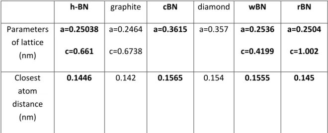
(13) Thèse de Théo Levert, Université de Lille, 2019. Chapter 1: Growth, transfer and characterization of graphene and h-BN Characteristics. Mechanical. Thermal. Parameter. Value. Young modulus. 0.5TPa. Compression Resistance. 300-560MPa. Specific heat @25°C. 700J.K-1.kg-1. Thermal conductivity @20°C. 2000-5000 W.m1.K-1. Sublimation point. 4240°C. Bandgap Electrical Mobility. 0eV Up to 200000 cm²V-1s-1. Table 1: Major properties of graphene. I.3) h-BN. Boron nitride is a III-V material. Unless other III-N nitride materials, which most stable structure is wurtzite, BN has four stable structure: hexagonal BN (h-BN), cubic BN (cBN), wurtzite BN (wBN) and rhomboedral BN (rBN). The hexagonal structure is stable at room temperature, the cubic structure is stable at high temperature and the two others are metastable at high pressure. We will focus in this work on h-BN, due to its 2D nature and outstanding properties. Boron nitride is not a natural material. Its first synthesis was made in 1842 by Balmain[19], using the reaction of boric acid melted on potassium cyanide. Unfortunately, the material was very unstable, and researchers used hundred years before finding a stable phase as powder. Bore (Z=5) and nitrogen (Z=7) are situated around carbon (Z=6) in the periodic classification, BN and carbon materials have similar stable structures: h-BN has a similar structure to graphite and cBN has a similar structure to diamond. Table 2 shows the different parameters of lattices.. 12 © 2019 Tous droits réservés.. lilliad.univ-lille.fr.
(14) Thèse de Théo Levert, Université de Lille, 2019. Chapter 1: Growth, transfer and characterization of graphene and h-BN h-BN. graphite. cBN. diamond. wBN. rBN. Parameters of lattice (nm). a=0.25038. a=0.2464. a=0.3615. a=0.357. a=0.2536. a=0.2504. c=0.661. c=0.6738. c=0.4199. c=1.002. Closest atom distance (nm). 0.1446. 0.142. 0.1555. 0.145. 0.1565. 0.154. Table 2: Lattice parameters of the different allotropes of BN and carbon. Figure 4: Structure of c-BN, w-BN, r-BN and h-BN[20]. 13 © 2019 Tous droits réservés.. lilliad.univ-lille.fr.
(15) Thèse de Théo Levert, Université de Lille, 2019. Chapter 1: Growth, transfer and characterization of graphene and h-BN h-BN phase is very similar to graphite with close lattice parameters (a=0.2464nm and c=0.6738nm for graphite). Its structure is formed by sheets stacked with an ABAB type. However, the difference of chemical nature of B and N atoms in the plane make the stack atoms perfectly on atoms (contrary to graphite) alternately with B and N. The force between the different sheets is a Van der Waals type. The distance between two planes is 3.3Å and the hexagons in the different sheets are made by BN covalent bonds with a distance of 1.45Å with a sp2 hybridization. The force of the covalent bond in the plane is much higher than the Van der Waals force between the sheets, giving at this material its peculiar properties. h-BN is a nontoxic material. We can use it at high temperature (850-900°C if presence of oxidation), which is quite higher than graphite (oxidation at 600°C. Moreover, it is transparent for visible light, making it a material of choice for transparent electronics. Its main physical properties are very close to graphene’s one, with a high mechanical robustness, a good thermal conductivity. However, h-BN is a semiconductor with a wide bandgap (5-6eV), making it a good substrate for electronics. Some theoretical studies on electronic properties of h-BN showed that its bandgap is first-order independent of the details of the atomic structure. Its dimensions are really close to the one of graphene (mismatch around 1.7%). Thus, many studies interested in the realization of heterostructures such as graphene/h-BN or sandwiches h-BN/graphene/h-BN for the realization of graphene field effect transistors (GFETs) or graphene/h-BN/graphene for the realization of tunneling field effect transistors. It must be noticed that h-BN, as well as graphene has a good thermal conductivity, which is a very important point for our work. Most physical properties of h-BN are presented in Table 3:. 14 © 2019 Tous droits réservés.. lilliad.univ-lille.fr.
(16) Thèse de Théo Levert, Université de Lille, 2019. Chapter 1: Growth, transfer and characterization of graphene and h-BN. Characteristics. Parameter Young modulus. Mechanical. Thermal. Electrical. Value (graphene). Value (h-BN). 0.5TPa. 0.7-1TPa. Compression Resistance. 30-120MPa. Specific heat @25°C. 800-2000J.K-1.kg-1. 700J.K-1.kg-1. Thermal conductivity @20°C. 1700-2000W.m-1.K-. 2000-5000 W.m1.K-1. Sublimation point. 2600-2800°C. Static dielectric constant. 7.04(⊥)-5.09(//). 1. High frequency dielectric constant. 4.95(⊥)-4.1(//). Bandgap. 4.97eV. 300-560MPa. 4240°C. 0eV. Table 3: Principal physical properties of h-BN and graphene[21]. 15 © 2019 Tous droits réservés.. lilliad.univ-lille.fr.
(17) Thèse de Théo Levert, Université de Lille, 2019. Chapter 1: Growth, transfer and characterization of graphene and h-BN. II). Growth and transfer of 2D graphene. 1) CVD growth of graphene. The CVD growth of graphene depends mainly on two things: a catalyst, which is in most case a transition metal such as Cu, Ni, Pt, Co, Au, Fe, Ru, Ir, Pd… and a precursor, which corresponds to the source of carbon forming the graphene on the catalyst. The catalysts mainly used are methane, ethylene or benzene. The total procedure of the graphene growth of graphene by CVD is always the same for every catalyst, namely a heating step, an annealing of the catalyst, then the growth step with the injection of the precursors at a constant temperature, then a cooling step down to room temperature. The Figure 5 shows a schematic of these four steps. Temperature. Heating. Annealing. Growth. Cooling. Time. Figure 5: Schematic of the four steps of a CVD growth of graphene. 16 © 2019 Tous droits réservés.. lilliad.univ-lille.fr.
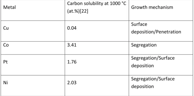
(18) Thèse de Théo Levert, Université de Lille, 2019. Chapter 1: Growth, transfer and characterization of graphene and h-BN. Table 4: Carbon solubility and the growth mechanism on typical metals for CVD graphene:. Metal. Carbon solubility at 1000 °C Growth mechanism (at.%)[22]. Cu. 0.04. Surface deposition/Penetration. Co. 3.41. Segregation. Pt. 1.76. Segregation/Surface deposition. Ni. 2.03. Segregation/Surface deposition. The growth mechanisms of graphene are depending on the catalyst, the precursor and the growth conditions. It is especially the solubility of the precursor which is the main factor. If the transition metal has a high carbon solubility (such as Ni), then after the growth and before the cooling there will be graphene at the surface of the metal, but also some carbon dissolved in the bulk material. When the temperature decreases, the carbon atoms dissolve in the metal will be evacuated and reached the surface of the metal, forming substantial layers of graphene. As a result, it is more complicated to obtain a monolayer of graphene with metals with a high carbon solubility such as Ni than a metal with a low carbon solubility such as Cu. Table 4 shows the solubility of few transition metals. The growth mechanism determines the interaction between the graphene and the catalyst. Batzill et al.[23] showed that there are three different mechanisms: Surface deposition, penetration and segregation. Table 4 shows the different mechanisms involved for some transition metals used. It must be noticed that these growth mechanisms are also depending on the temperature. We will concentrate on the growth of graphene on Cu and Ni, which are the two metals used in this work. The main advantage of the Cu as a catalyst is its low solubility of carbon. Indeed the Cu is not a carbon “tank” after the growth, so very few carbon atoms will segregate at the Cu surface during the cooling, making it a good candidate for the growth of graphene monolayer[24]. However, it is less reactive than Ni and it requires temperature around 17 © 2019 Tous droits réservés.. lilliad.univ-lille.fr.
(19) Thèse de Théo Levert, Université de Lille, 2019. Chapter 1: Growth, transfer and characterization of graphene and h-BN 1000°C to observe dissociation of the precursor at its surface, which is close to the sublimation temperature of Cu. Thus, it is very important to have a good control of the growth in order to avoid the sublimation of the copper foil in the CVD system. The growth principle of graphene on copper is a heating up to the growth temperature under a H2 flow, in order to increase the size of the Cu grains (which can be as big as 2mm under low pressure). Once the growth temperature reached, we insert the precursor in the CVD system, which will dissociate on the surface of the copper foil, leading into a saturation in carbon at the surface of the copper foil. As a result, we can observe the nucleation of graphene on the surface of the copper foil and an expansion of the graphene domains until they reach each other. Thereby we obtain a continuous layer of graphene, electrically continuous but with several domains, with the possibility of different orientations of the domains. Then we perform the cooling down to the room temperature. In most of the case the growth of graphene on copper leads to the formation of a monolayer due to the reasons explained previously, but in bad growth conditions (flow of the precursor to high or growth time too long) we can observe the formation of multilayers at the nucleation spots.. Figure 6: Schematic of the CVD growth of graphene on copper[25]. Ni as a catalyst has not been studied as much as the copper because the control of the number of layers and the uniformity of the growth is really hard because of the high solubility of carbon in nickel. However Nickel is still a good candidate for the graphene growth because the dissociation of the precursor occurs at lower temperature[26]. The growth of graphene on nickel consists on an increase of the temperature up to the temperature growth under a H2 flow in order to increase the size of the nickel grains[27]. When the growth temperature is reached, we insert the precursor into the CVD system. First the carbon dissolves into the nickel and then nucleation spots appeared at the surface of the nickel and the graphene growth begins. After some time, we stop the precursor exposure and we start the cooling. During this cooling, depending on the growth 18 © 2019 Tous droits réservés.. lilliad.univ-lille.fr.
(20) Thèse de Théo Levert, Université de Lille, 2019. Chapter 1: Growth, transfer and characterization of graphene and h-BN temperature and the temperature rate, we can observe the segregation of the carbon inside the Ni at the surface, leading to the formation of multilayers of graphene at the surface.. Figure 7: Schematic of the CVD growth of graphene on nickel[28]. 2) Characterization of graphene. The quality of graphene varies depending on the growth parameters, the choice of the precursor or the catalyst. Thus, it is important to systemically control the quality of graphene to validate or not the growth conditions. Several techniques have been developed and adapted for graphene. For our work we focused on 3 main characterization techniques: Optical microscopy, scanning electron microscopy (SEM) and Raman spectroscopy.. 19 © 2019 Tous droits réservés.. lilliad.univ-lille.fr.
(21) Thèse de Théo Levert, Université de Lille, 2019. Chapter 1: Growth, transfer and characterization of graphene and h-BN a) Optical microscopy. Optical microscopy is a good way to observe graphene. Indeed, the association of an optical microscope with a specificity of the substrate allows a good and quick identification of graphene. In this work we chose to transfer graphene onto SiO 2/Si substrates. The optical contrast results from light interferences inside the SiO 2. The thin oxide layer acts as a Fabry Perrot cavity. The transfer of graphene on such substrates for specific SiO2 thickness increases the optical contrast and allows us to identify the graphene with this simple method[29]. The following figure shows the optical contrast as a function of the wavelength and the SiO2 thickness.. Figure 8: Optical contrast of graphene as a function of the wavelength and the SiO2 thickness[29]. We can see that the optical contrast of graphene is at his maximum at thickness of SiO2 of 90 and 285nm for a 55nm wavelength (which corresponds to the maximum of sensibility of human eyes). Thus, we chose to work with substrate with a thickness of SiO2 at around 280-300nm. The observation of transferred samples with optical microscopy allows us to confirm its presence but also to evaluate quickly its quality, with the formation for example of holes or cracks during the transfer. Figure 9 shows an example of graphene transferred onto SiO2.. 20 © 2019 Tous droits réservés.. lilliad.univ-lille.fr.
(22) Thèse de Théo Levert, Université de Lille, 2019. Chapter 1: Growth, transfer and characterization of graphene and h-BN. Figure 9: Example of optical image of graphene on SiO2. However, this technique does not help for the identification of the number of layers of graphene or the crystallinity quality of graphene, letting us use other technique such as SEM, AFM and Raman spectroscopy.. b) Scanning Electron Microscopy. Scanning electron microscopy (SEM) is a quick and nondestructive technique to observe samples at high magnification. It is based and electron-material interaction. The principle of SEM is based on a scan of a sample with an electron beam and the detection of back electrons point by point, in order to create a cartography of all the scanned surface. The secondary electrons coming on the detector are coming from a zone at around 10nm on the surface of the sample and are really sensitive to the topography. The lateral resolution is close to the diameter of the electron beam (few nm), resulting in high magnification of the collected images. SEM is an important tool for morphological characterization and has no constraint concerning the size of the sample.. 21 © 2019 Tous droits réservés.. lilliad.univ-lille.fr.
(23) Thèse de Théo Levert, Université de Lille, 2019. Chapter 1: Growth, transfer and characterization of graphene and h-BN. Figure 10: a) Schematic diagram of the SEM working principle[30] and b) SEM image of graphene on SiO2. c) Raman spectroscopy. Raman spectroscopy is a non-destructive characterization technique, which is a great advantage for the study of graphene. Moreover, it is a technique pretty fast to use and requires no preparation of the sample. This technique has been discovered in 1928 by Chandrasekhar Raman[31] and is based on the interaction of the inelastic scattering of a monochromatic light and the molecular vibrations of the studied material (i.e photonphonon interaction). The principle consists of focalizing a monochromatic light source (usually from a laser) and to analyze the diffused light. Indeed, the material is set at a virtual level of energy by the scattering of the coming photons. The material emits back the photons with a different energy level. This back scattering shows two types of signals: -. Rayleigh scattering which is an inelastic scattering of the coming photons without a change of energy level. Stokes scattering (or anti-Stokes scattering) in the case where the coming photons interact with the phonons of the studied material with respectively a gain or a loss of energy level. The observed variation of energy gives us the levels of energy of rotation and vibration of the molecules of the studied material.. This energy variation is analyzed by a photodetector. It is called Raman shift. A Raman spectrum shows the diffused Raman intensity as a function of the frequency difference of the coming and the back scattering: if we study the Stokes scattering, this difference is 22 © 2019 Tous droits réservés.. lilliad.univ-lille.fr.
(24) Thèse de Théo Levert, Université de Lille, 2019. Chapter 1: Growth, transfer and characterization of graphene and h-BN positive and zero for the Rayleigh scattering. For practical reasons, this frequency difference is converted in wavenumber 𝜈̅ by the following formula: 𝜈̅ =. 1 𝜈 = 𝜆 𝑐. With 𝜈̅ : wavenumber (in cm-1), 𝜆 : wavelength of the scattering (in cm), 𝜈 : frequency of the scattering (in Hz) and c : speed of light in vacuum. Utilization of Raman spectroscopy for carbon materials is not new[32] and especially for graphene[33]. Raman spectrum of graphene are composed of 3 main peaks: G, D and 2D peaks, which can be seen in Figure 11. Figure 11: Example of Raman spectra of graphene[34]. -. -. G peak (around 1590cm-1): It is a characteristic signal of graphene and is associated with planar vibrations of sp2 carbon atoms. It corresponds to a Raman process of 1st order. It results from the phonons of E2g symmetry, which is associated to a shear stress in the unit cell plane. 2D or G’ peak (around 2700cm-1): it corresponds to a Raman process of 2nd order. In this configuration, there is a scattering of two phonons: one resulting from the electron scattering excited from a band close to the K point to a band close to the. 23 © 2019 Tous droits réservés.. lilliad.univ-lille.fr.
(25) Thèse de Théo Levert, Université de Lille, 2019. Chapter 1: Growth, transfer and characterization of graphene and h-BN. -. -. -. K’ point, and another one by the same process but on the other side. It corresponds to an intra-valley process. D peak (around 1350cm-1): it is a characteristic of the defects or disorder in the graphene plane, and is associated to out-of-plane vibrations. It corresponds to a Raman process of 2nd order with a phonon with a E2g symmetry and a defect of the system necessary for the activation of the D peak[35]. It comes from an elastic scattering of an excited electron from a band close to the K point to a band close to the K’ point on a defect, then a second scattering results in the emission of a photon. This peak is very weak or not present for a high quality graphene[36]. Two other peaks can also be detected: D’ peak and D+G peak: D+G peak (around 2940cm-1): This peak corresponds to a process with two phonons and a defect. It is a configuration where the scattering of the D and G peak scattering occur. In that case there is first an elastic scattering from a defect from a band close to the K point to a band close to the K’ point, and a 2nd inelastic scattering with a phonon emission. D’ peak (around 1635cm-1): This peak is resulting from an inelastic scattering from an excited electron because of a defect with a phonon emission.. -. Figure 12: Representation of the different Raman processes resulting in G peak(a), D' peak(b), 2D' peak(c), D peak(d) and 2D peak (e). Blue arrows are corresponding to the absorption of a photon by an electron. Red arrows correspond to the de-excitaion of an electron with a photon emission. Dotted horizontal lines represent an elastic scattering because of a defect and dotted arrows correspond to a scattering process[35]. 24 © 2019 Tous droits réservés.. lilliad.univ-lille.fr.
(26) Thèse de Théo Levert, Université de Lille, 2019. Chapter 1: Growth, transfer and characterization of graphene and h-BN Thus, the study of Raman spectrum of graphene (Figure 11) can inform us on the quality of the graphene (presence of defects), the number of layers, the doping level… Indeed, the Intensity ratio of some peaks allows us to determine the number of layers or to quantify the defects in graphene. For the number of defects in graphene, the intensity of D peak (ID) (characteristic for the defects) relatively to the G peak (IG) is relevant. A low ration ID/IG informs us on the low disorder in the graphene plane and so a good crystalline quality of the graphene. When working with a monolayer, one can observe the presence of a 2D peak very sharp and more intense than the G peak. When the number of layers increases, the 2D peak broadens itself and becomes less intense. Thus the ratio of intensity of G peak and 2D peak can informs us on the number of layers[37]. An intensity of the peak 2D 2 to 3 times higher than the intensity of the G peak informs us on the presence of a monolayer. This ratio is equal to 1 in the bilayer case and is superior to 1 over 2 layers. This method is quite simple to determine the number of layers of graphene.. 3) Growth of 2D polycrystalline graphene. As discussed earlier, we chose to focus on the growth of graphene using CVD, which is the better way to produce large area graphene for industry. We chose to use commercial Cu foil from Alpha Aesar of high purity (99,9999%) in order to obtain monolayer graphene, as discussed before. Graphene growth has been carried out in a Jipelec JetFirst Rapid Thermal CVD (RTCVD). This system allows heating and cooling at high rates (10°C/s). Heating is provided by halogen lamps on the top of the chamber and the sample placed horizontally onto a Si wafer. The temperature is measured by a thermocouple contacting the sample’s back face. The growth itself is decomposed as a heating, an annealing, a growth and a cooling. We used a mixture of 100sccm of Argon and 5sccm of Dihydrogen during all the steps and 20scccm of methane as a precursor during the growth phase. We can see a schematic of the steps in Figure 14. Note that the growth parameters have been optimized by postdoc Geeta.. 25 © 2019 Tous droits réservés.. lilliad.univ-lille.fr.
(27) Thèse de Théo Levert, Université de Lille, 2019. Chapter 1: Growth, transfer and characterization of graphene and h-BN. Figure 13: View of the CVD used for the growth of graphene. We first cut the Cu foil in small pieces (2.5x2.5cm), clean them with acetic acid for 5min, acetone for 5min and IPA for 5min under ultrasound in order to remove all possible copper oxide and to have the cleanest surface possible. We then put the pieces onto a Si wafer in the chamber. We proceed to a high vacuum (<5.10-5 bar) before starting and then we start the heating for 5min from room temperature to 300°C and then 2min from 300 to 1070°C, then the annealing for 5min, we continue with the growth for 5min and we finish with a quick cooling of the chamber using a water flow (with a decrease rate of 60°C/s from 1000 to 700°C), then around 10 min to reach room temperature.. Figure 14: Schematics of the growth parameters. 26 © 2019 Tous droits réservés.. lilliad.univ-lille.fr.
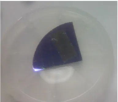
(28) Thèse de Théo Levert, Université de Lille, 2019. Chapter 1: Growth, transfer and characterization of graphene and h-BN 4) Characterization of the grown graphene. An optical image of the as-grown graphene can be seen in Figure 15. The dark lines are the Cu grain boundaries. It can be seen that no grain boundaries of graphene can be seen, indicating that we obtained a full covered sample. No particles or copper oxide have been observed on our samples, indicating a good quality of the copper foil and a good cleaning of the surface before the growth.. Figure 15: a) Photography and b) Optical image of graphene on Cu. SEM images have been performed using a Zeiss Ultra 55. The SEM images at low and higher magnification are also indicating that we have a full covered sample, confirming the growth conditions. We can also notice the presence of few nanoparticles on some points of the Cu foil, which surely comes from the quality of the Cu foil, or the cleaning of the foil.. 27 © 2019 Tous droits réservés.. lilliad.univ-lille.fr.
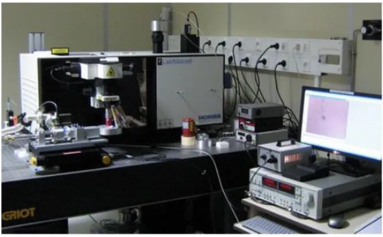
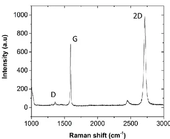
(29) Thèse de Théo Levert, Université de Lille, 2019. Chapter 1: Growth, transfer and characterization of graphene and h-BN. Figure 16: SEM images of graphene on copper foil. However, at higher magnification, at some areas of the surface, we noticed some darker area, indicating the presence of multilayer graphene at the nucleation points, as explained earlier concerning the formation of graphene on copper foil. Nevertheless, the objective of obtaining graphene on all available surface is achieved with these growth conditions, letting us work with large area graphene (3x3cm). Raman spectroscopy has been carried out using a LabRAM HR Horiba Jobin-Yvon with a 473nm laser as the light source, as we can see in Figure 17:. Figure 17: Photography of the Raman system used in this work. 28 © 2019 Tous droits réservés.. lilliad.univ-lille.fr.
(30) Thèse de Théo Levert, Université de Lille, 2019. Chapter 1: Growth, transfer and characterization of graphene and h-BN Raman has been performed on the as-grown sample. We can clearly identify the G and 2D peaks at respectively 1581 and 2712cm-1 for a FWHM of 29 and 45cm-1, and a weak D peak at 1355cm-1, indicating a high quality graphene. The relative intensities of the G and 2D peak is around 2.1, which is really close to 2, indicating the presence of monolayer graphene. One can notice that we obtained similar spectrum on all available surface of the copper foil, making the sample very homogeneous.. Figure 18: Raman spectra of graphene on copper foil. Thus, we showed that we obtained the good conditions to achieve full covered pieces of copper foil with monolayer graphene of good quality.. 5) Transfer of 2D graphene. a) Method of transfer. Various transfer methods are currently developed to prepare graphene onto dielectric substrates for device fabrication. One way to reach this goal is to cover the graphene with a polymer supporting layer (PMMA, for example) to prevent graphene from collapsing, and then etch the underneath Cu foil. Besides increasing visibility and facilitating 29 © 2019 Tous droits réservés.. lilliad.univ-lille.fr.
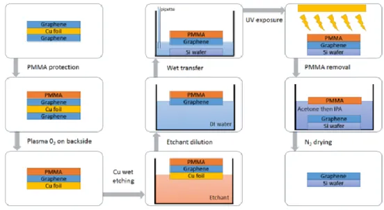
(31) Thèse de Théo Levert, Université de Lille, 2019. Chapter 1: Growth, transfer and characterization of graphene and h-BN the handling, the supporting layer is also necessary as bare graphene may collapse due to surface tension. The wet transfer technique consists on several steps which have been compiled according to what have been done in literature. We first cover the graphene/Cu foil with PMMA and we then perform an annealing at 110°C with a very slow heating and cooling in order to prevent cracks in the graphene due to the difference of the thermal expansion coefficient between copper and graphene. Then we perform an etching of the back graphene at the bottom of the copper foil using an O2 plasma[38]. The next step is to etch the copper foil. In that aim we use a solution of ammonium persulfate ((NH4)2S2O8), known as a good and clean etchant of copper and copper oxide nanoparticles residues[39] with a concentration of ~200mol.L-1 (see appendix for details). We let the PMMA/graphene/Cu float on the surface of the solution. We let the copper being etched for several hours (up to 15h) and we take the floating PMMA/graphene to put it in a DI solution. We repeat this operation around 10 time in order to rinse the graphene from the etchant solution. We can then use a SiO2 wafer to collect the PMMA/graphene on the top of its surface, by placing the Si wafer at the bottom of the container and removing the remaining water with a pipette until the PMMA/graphene reach the surface of the wafer. We perform again an annealing at 90°C with a slow heating and cooling in order to evaporate all water remaining. For the PMMA removal we first expose our sample to deep UV to facilitate the removal[40]. We then put our sample in different baths of acetone then IPA to remove the PMMA. A schematic of the wet transfer can be found in Figure 19, and the detailed parameters of each step can be found in Annex.I.. 30 © 2019 Tous droits réservés.. lilliad.univ-lille.fr.
(32) Thèse de Théo Levert, Université de Lille, 2019. Chapter 1: Growth, transfer and characterization of graphene and h-BN. Figure 19: Schematic of the wet transfer technique used in this work. b) Characterization of transferred graphene. The wet transfer process described earlier has been used on our sample in order to achieve a clean transfer of graphene. Figure 20 shows graphene coated with PMMA transferred onto SiO2 before the removal of the PMMA. We can see that the graphene finds itself very flat on the Si wafer, with absence of bubbles or cracks.. 31 © 2019 Tous droits réservés.. lilliad.univ-lille.fr.
(33) Thèse de Théo Levert, Université de Lille, 2019. Chapter 1: Growth, transfer and characterization of graphene and h-BN. Figure 20: Optical image of graphene with PMMA transferred on SiO2/Si. After the transfer of graphene, our sample have been slowly annealed, and then we proceeded to the PMMA removal, according to our process. Then it is possible to observe the transferred graphene using an optical microscope, according to the reasons discussed in a). Thus, it is possible to proceed to a first check of the graphene quality. Figure 21 shows the absence of cracks or bubbles either at the border or at the center of the sample, and also the absence of remaining resist residue, indicating that we achieved a clean transfer of graphene.. 32 © 2019 Tous droits réservés.. lilliad.univ-lille.fr.
(34) Thèse de Théo Levert, Université de Lille, 2019. Chapter 1: Growth, transfer and characterization of graphene and h-BN. Figure 21: Optical images of graphene transferred on SiO2 a) at the border of the sample and b) in the center of the sample. At higher magnification, using a SEM, we can also confirm the quality of the transfer as we can see in Figure 22. However, at higher magnification we can observe the presence of small wrinkles, which can lead into lowering the electronic transport of our graphene. However, the concentration of wrinkles or defects is very low. Further ameliorations on the growth can be investigated.. Figure 22: SEM images of graphene transferred on SiO2. 33 © 2019 Tous droits réservés.. lilliad.univ-lille.fr.
(35) Thèse de Théo Levert, Université de Lille, 2019. Chapter 1: Growth, transfer and characterization of graphene and h-BN. Figure 23: Raman spectra of the 3DC foam. Raman has been performed on the transferred sample as we can see in Figure 23. We can clearly identify clearly the G and 2D peaks at respectively 1590 and 2717cm-1 for a FWHM of 12.4 and 37.5cm-1, and a weak D peak at 1360cm-1, indicating a high quality graphene. The relative intensities of the G and 2D peak is around 1.5, indicating the presence of monolayer graphene. The position of the peaks did not change much compared to the spectra with graphene on copper foil. However, the relative intensities of the G and 2D peaks changed a bit, indicating residual stress in the film. This might be explained by the annealing of graphene on copper foil before the transfer because of the difference of the thermal expansion coefficient between graphene and copper. The low values of FWMH of G and 2D peaks and the absence of peak at 2900cm-1 indicates a clean removal of the PMMA, as compared to one can see in literature[41]. It has to be noticed that we obtained similar spectrum on all available surface of the copper foil, making the sample very homogeneous. This validates also the transfer process used in this work.. 34 © 2019 Tous droits réservés.. lilliad.univ-lille.fr.
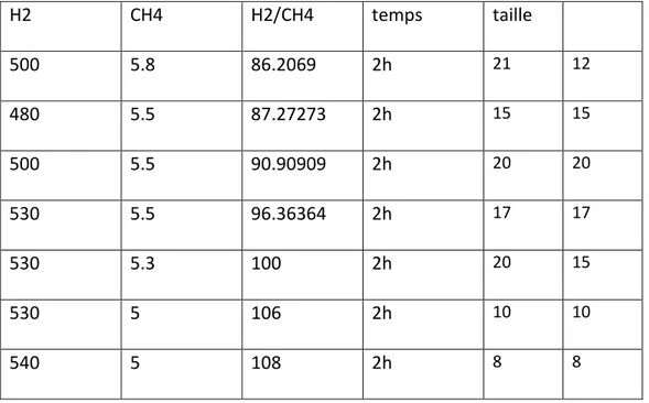
(36) Thèse de Théo Levert, Université de Lille, 2019. Chapter 1: Growth, transfer and characterization of graphene and h-BN 6) Growth of 2D monocrystalline graphene. Polycrystalline graphene present some lack of electron mobility because of the different orientations of the grains and the grain boundary, modifying the band structure of graphene, resulting in electron mobility lower than mobility of crystalline materials[42]. One way to bypass this problem is to use single crystals of graphene. Thus, it requires large single crystals of graphene in order to be compatible with microelectronic processes. The typical size of single crystals of graphene can be as large as millimeter size under special conditions but a lot of works present typical size around 10µm , and are usually reported with high nucleation points density (~106cm-2), limiting the size of the grains[43]. It is a challenge to reduce the nucleation density. Several approaches have been proposed, such as the use of copper oxide[44], the use of Pt as catalyst[45], or electro polishing of the copper foil[46]. We chose to treat the surface of the copper foil with a long annealing (3H) at atmospheric pressure using a strong H2 flow (~600sccm). It appeared that we reduced the nucleation density down to 4x104cm2 as we can see in Figure 24.. Figure 24: SEM image of single crystals graphene. With this low nucleation density, we chose to change firstly the H2/CH4 ratio, keeping the growth time at 2H in order to obtain large single crystals. The different. 35 © 2019 Tous droits réservés.. lilliad.univ-lille.fr.
(37) Thèse de Théo Levert, Université de Lille, 2019. Chapter 1: Growth, transfer and characterization of graphene and h-BN parameters used in this goal are resumed in Erreur ! Source du renvoi introuvable. with the corresponding average size of single crystals. H2. CH4. H2/CH4. temps. taille. 500. 5.8. 86.2069. 2h. 21. 12. 480. 5.5. 87.27273. 2h. 15. 15. 500. 5.5. 90.90909. 2h. 20. 20. 530. 5.5. 96.36364. 2h. 17. 17. 530. 5.3. 100. 2h. 20. 15. 530. 5. 106. 2h. 10. 10. 540. 5. 108. 2h. 8. 8. The different sizes of the grain as a function of H2/CH4 ratio are presented in Figure 25. It has to be noted that the biggest grain size is around 20µm for a H2/CH4 ratio, corresponding to the best etching/graphene growth ratio. It is very similar to other work on the role of H2 flow on graphene growth[47].. Figure 25: Average size of the grains as a function of the H2/CH4 ratio. 36 © 2019 Tous droits réservés.. lilliad.univ-lille.fr.
(38) Thèse de Théo Levert, Université de Lille, 2019. Chapter 1: Growth, transfer and characterization of graphene and h-BN Knowing the best H2/CH4 ratio, we chose to increase the growth time up to 5H to check the role of the growth time on the size of the grains. Different growth parameters are resumed in Table 5. It appeared that the best growth time was 4H. After 5H the size of the single crystals didn’t increase, indicating that the etching and graphene growth competition achieved its saturation regime, resulting in the limitation of the size of single crystals.. H2 flow (sccm). CH4 flow (sccm). H2/CH4 ratio. time (H). Size (µm). 500. 5.5. 90.9. 2. 20. 500. 5.5. 90.9. 3. 22. 500. 5.5. 90.9. 4. 28. 500. 5.5. 90.9. 5. 27. Table 5: Growth conditions of single crystals graphene. We presented the SEM image of our best sample in Figure 26.. Figure 26: SEM image of single crystal graphene. 37 © 2019 Tous droits réservés.. lilliad.univ-lille.fr.
(39) Thèse de Théo Levert, Université de Lille, 2019. Chapter 1: Growth, transfer and characterization of graphene and h-BN We checked the Raman signal of our grown graphene. We can identify clearly the G and 2D peak at 1579.9 and 2707.9cm-1 respectively with a, intensity ratio of 2.3, confirming the presence of monolayer graphene. Moreover, the very weak D peak indicates a high quality graphene with very few defects.. Figure 27: Raman spectra of single crystal graphene. We achieved a maximum size of ~30µm, but other studies showed bigger single crystals (up to 5mm) and lower nucleation density using other methods[44],[48],[45]. Thereby we decided to stop the investigations at this time.. III). Growth of 3D graphene. 1) Growth of graphene on Nickel foam. The growth process used in this work is very similar to the growth of 2D graphene and then the growth mechanism will not be explained in detail. It consists to use a Nickel foam as a substrate which is well known for growth of multilayer graphene[49]. The substrate used for the growth of both 3DC and 3DBN is a Nickel foam from Latech[50]. It is a porous Ni foam with a purity higher than 99%, with a porosity between 90 to 98% and a pore concentration of around 100 pores per inch (PPI). An SEM image of the structure of the foam can be seen in Figure 28: 38 © 2019 Tous droits réservés.. lilliad.univ-lille.fr.
(40) Thèse de Théo Levert, Université de Lille, 2019. Chapter 1: Growth, transfer and characterization of graphene and h-BN. Figure 28: SEM image of the Ni foam[50]. The 3DC growth process is very similar to those of 2D graphene. It consists to expose the Nickel substrate to a mixture of dihydrogen and argon for the annealing, and a mixture of dihydrogen, argon and methane (which is the precursor) for the growth in a CVD system at atmospheric pressure[51] (APCVD). A schematic of the growth process of 3DC can be seen in Figure 29.a). The growth mechanism explained earlier allows the multilayer graphene to deposit on all available surface of the Nickel foam, adopting its porous structure. After the growth, the foams obtained are then dip coated with PMMA, in order to protect the h-BN or the graphene and then dipped into an HCl solution for several hours (at least 15h) for the etching of the Nickel. After total etching of the Nickel, the foams are rinsed with DI water for few hours and then dried. The resulting 3D foam is then put into a slow annealing during 3h with a temperature of 700°C and a rate of 300°C/h in order to evaporate the PMMA coating (BN and graphene are stable at that temperature). This annealing allows us to prevent the use of classical dissolution of the resist in a solvent such as acetone, avoiding the resist residues issue[52]. After the annealing, we obtain pure foam of 3DC, with a similar structure and porosity to the Nickel foam used. Optical images of 3DC can be seen in Figure 29.b).. 39 © 2019 Tous droits réservés.. lilliad.univ-lille.fr.
(41) Thèse de Théo Levert, Université de Lille, 2019. Chapter 1: Growth, transfer and characterization of graphene and h-BN. Figure 29: a) Schematic process of the growth of 3DC and b) image of a 3DC foam. 2) Characterization of the Foam. In order to characterize the obtained 3DC, SEM images have been obtained and can be seen in Figure 30. Thus, we can see that the foams obtained has a similar structure and the same porosity as the Nickel foam used at first. At a higher magnification, we can see the presence of several domains, with some grain boundaries and some wrinkles. This results from the difference of the thermal expansion between graphene and the Ni foam, also observed in previous work[51].. Figure 30: SEM images of the 3DC foam. 40 © 2019 Tous droits réservés.. lilliad.univ-lille.fr.
(42) Thèse de Théo Levert, Université de Lille, 2019. Chapter 1: Growth, transfer and characterization of graphene and h-BN. Raman spectroscopy has been performed on the obtained foams and the spectrum can be seen in Figure 31. We can clearly identify the presence of the G and 2D peak located at 1582 and 2700cm-1 with a FWHM of 25.7 and 59.0cm-1 respectively. The intensity ratio of 0.72 indicates the presence of multilayer graphene. Moreover, the low intensity of the D peak on the graphene indicates the obtained graphene is of high quality according to the domain’s sizes with few defects. Elsewhere, the change of intensity of the obtained peaks on few other points indicates that graphene is not homogeneous. This can be explained by the use of a Nickel foam which results in a few layers graphene[53] giving several domains with a different number of layers, with higher number of layers near the nucleation points, as we can see in Figure 31.. Figure 31: Raman spectrum of 3DC on two different points. IV). Growth of 2D h-BN. 1) CVD growth of h-BN. Many methods have been used to synthetize h-BN of various quality. They are very similar to what have been achieved for the growth of graphene with some modifications, especially concerning the precursors. We will focus on the growth of hBN by CVD.. 41 © 2019 Tous droits réservés.. lilliad.univ-lille.fr.
(43) Thèse de Théo Levert, Université de Lille, 2019. Chapter 1: Growth, transfer and characterization of graphene and h-BN Similarly, metals that can be used as catalyst for the growth of h-BN such as Ni, Cu, Co, Ru, Pt… The most commonly used precursor are ammonia borane[54] (NH3BH3), borazane[55] (BNH6), borazine[56] or the combination of ammonia and diborane. All those precursors are either solid or liquid but have a common point: they are all easily evaporable by moderate heating and thus are perfect candidate for CVD process. A schematic of a h-BN growth can be found in Figure 32. As for graphene, micrometerssized monolayers of h-BN have been grown by other work using Cu and Co substrates[57]. Indeed, the solubility of B and N are similar on those metals, in the same way as for C. However, there is some issues providing large area h-BN (wafer scale) with a good quality, either if it is multilayer or monolayer, providing a great challenge for applications in electronics. Indeed, the use of h-BN as a substrate requires large area and a very flat surface.. Figure 32: Schematic of the CVD of h-BN using a copper foil as a catalyst and ammonia borane as a precursor[58]. 42 © 2019 Tous droits réservés.. lilliad.univ-lille.fr.
(44) Thèse de Théo Levert, Université de Lille, 2019. Chapter 1: Growth, transfer and characterization of graphene and h-BN For now, only few micrometers-sized of single crystals of h-BN have been achieved in literature. We will focus on the growth of polycrystalline h-BN in order to obtain large area for applications in electronics.. Figure 33: Atomic force microscopy image of a trigonal monolayer h-BN grain grown on Cu foil[57]. 2) Growth of 2D polycrystalline h-BN. We chose to focus on the growth of polycrystalline h-BN using CVD, which is the better way to produce large area h-BN for industry. We chose to use commercial Cu foil from Alpha Aesar of high purity (99,9999%) in order to obtain monolayer h-BN, as discussed before. h-BN growth has been carried out in a Thermo Scientific Lindberg CVD, which can be seen in Figure 34. This system allows heating and cooling at moderate rates with 2 inches tube furnace. We used a mixture of 200sccm of Argon and 20sccm of Dihydrogen during all the steps. We chose a solid precursor of ammonia borane and we decided to change the amount of precursor from 6 to 11g during the growth phase. The precursor is placed at the entrance of the tube and heated at ~90°C during the growth phase. We first cut the Cu foil in small pieces (6x2cm), clean them with acetic acid, acetone and IPA under ultrasound in order to remove all possible copper oxide and to have the 43 © 2019 Tous droits réservés.. lilliad.univ-lille.fr.
(45) Thèse de Théo Levert, Université de Lille, 2019. Chapter 1: Growth, transfer and characterization of graphene and h-BN cleanest surface possible. We then put the pieces in the middle of the tube furnace. We proceed to a high vacuum (<5.10-5 bar) before starting and then we start the heating for 40min from room temperature to 1000-1050°C, then the annealing for 1H, we continue with the growth for 30min and we finish with a moderate cooling by stopping the heater and let the temperature of the tube decrease down to room temperature. A schematic of the growth process can be found in Figure 35.. Figure 34: Image of the tubular CVD used in this work. 1050 °C. Annealing. H2 + Ar. 40 min. H2 + Ar. 1H. Growth. H2 + Ar + NH3BH3 30 min. Figure 35: Schematic of the growth process of h-BN. 3) Characterization of the grown h-BN. 44 © 2019 Tous droits réservés.. lilliad.univ-lille.fr.
(46) Thèse de Théo Levert, Université de Lille, 2019. Chapter 1: Growth, transfer and characterization of graphene and h-BN For all the different growth made, we performed optical images, SEM images, and Raman spectroscopy. The optical images and the SEM images of our samples tends to show that we have full covered h-BN. We first tried to vary the quantity of precursor from 6 to 11g to achieve good growth conditions. For the growth with a low quantity of precursor (68g of ammonia borane) no Raman spectra have been obtained, indicating bad quality of the h-BN. From 9 to 11g of ammonia borane, a weak Raman signal has been obtained at ~1370cm-1 as observed in literature[59],[60], indicating the presence of h-BN. However, for samples with high quantity of precursor we observed the presence of multilayer at the nucleation point, as we can see in the following SEM image:. Figure 36: SEM image of h-BN on copper foil with the presence of multilayer regions. All these growths have been carried out with a growth temperature of 1050°C.. Table 6 shows the different observations made with the help of Raman spectroscopy and SEM images. The best quantity of precursor seems to be 9g of ammonia borane.. Quantity of Ammonia borane (g). Raman signal. SEM observations. 6. No signal. Seems full covered 45. © 2019 Tous droits réservés.. lilliad.univ-lille.fr.
(47) Thèse de Théo Levert, Université de Lille, 2019. Chapter 1: Growth, transfer and characterization of graphene and h-BN 7. No signal. Seems full covered. 8. Weak signal. Seems full covered. 9. Good signal. Seems full covered. 10. Good signal. Seems full covered with the presence of multilayer regions. 11. Good signal. Seems full covered with the presence of multilayer regions. Table 6: Observations of the characterized samples made with Raman spectroscopy and SEM with different quantity of precursor. We chose to present the best sample that we grew, according to the characterization performed, using 9g of ammonia borane. The samples have been cut into 3 pieces of ~2cmX2cm. Two pieces have then been transferred and characterized. We will focus now on these two pieces, named sample 1 and sample 2 in the following description. We can see that the two samples are very similar and have the same size. We can also see at optical microscope that the copper is homogenous, with similar copper grain size.. 46 © 2019 Tous droits réservés.. lilliad.univ-lille.fr.
(48) Thèse de Théo Levert, Université de Lille, 2019. Chapter 1: Growth, transfer and characterization of graphene and h-BN. Figure 37: Optical images of sample 1 and sample 2. Figure 38: Optical images of h-BN on copper. The SEM images at low and higher magnification are also indicating that we have a full covered sample, confirming the growth conditions, with similar structure of grains and grains boundaries.. 47 © 2019 Tous droits réservés.. lilliad.univ-lille.fr.
(49) Thèse de Théo Levert, Université de Lille, 2019. Chapter 1: Growth, transfer and characterization of graphene and h-BN. Figure 39: SEM images of h-BN on copper. Raman spectroscopy has been performed on our samples. We chose different areas to compare the Raman signal on all surfaces. For both samples we found similar Raman spectrum with the typical peak of h-BN located at 1370cm-1 originating from the boronnitrogen bond stretching. Although the signal is pretty weak, it is comparable with other publications on monolayer h-BN[59],[60]. The FWMH of the peak is always around 5-7cm1. The position of the peak and the FWMH seem confirming the presence of a monolayer of h-BN[61]. Moreover, we obtained similar spectrum on all available surface, confirming the good conditions of the growth to obtain a full covered film of h-BN. Figure 40: Different Raman spectrum performed on h-BN on copper. Sample 1. 48 © 2019 Tous droits réservés.. lilliad.univ-lille.fr.
(50) Thèse de Théo Levert, Université de Lille, 2019. Chapter 1: Growth, transfer and characterization of graphene and h-BN. Figure 41: Different Raman spectrum performed on h-BN on copper. Sample 2. XPS spectroscopy was carried out on our sample with the Help of Dominique Vignaud and Jawad Hadid in order to determinate the elemental composition and the stoichiometry of our h-BN. We attributed the 397.6 and 190.1eV peaks to N1s and B1s respectively, as expected for h-BN[59], confirming the presence of a pure h-BN sample.. Figure 42: XPS spectra of h-BN on copper. 49 © 2019 Tous droits réservés.. lilliad.univ-lille.fr.
(51) Thèse de Théo Levert, Université de Lille, 2019. Chapter 1: Growth, transfer and characterization of graphene and h-BN. Figure 43: Peak parameters from the XPS signal. 4) Transfer and characterization of h-BN. A good and clean transfer of h-BN is essential for potential applications in electronics. Thus, we tried to use what have been achieved with the graphene transfer and to adapt it to the transfer of our samples of h-BN. We will present a second method of transfer called bubbling transfer which has been optimized by another PhD student (Soukaina BEN SALK from CARBON group) on graphene. We will present the characterization performed on the two best samples presented earlier.. a) Method of transfer. Two methods of transfer have been used: the wet transfer and the bubbling transfer. First, we adapted the wet transfer of graphene with h-BN. Several improvements have been made. Due to the difference of surface tension between graphene and h-BN, we modified the deposition parameters of PMMA to achieve a protection layer of the same thickness. As h-BN is less chemically active than graphene, an O2 plasma etching of the back face is not suitable (chemical etching). We preferred to use an Ar etching (physical etching). 50 © 2019 Tous droits réservés.. lilliad.univ-lille.fr.
(52) Thèse de Théo Levert, Université de Lille, 2019. Chapter 1: Growth, transfer and characterization of graphene and h-BN We checked with Raman spectroscopy that the back side was fully etched from h-BN. The other steps of the wet transfer remain the same as for graphene and can be found in Figure 19. An optical image of sample 1 before and after wet transfer can be found in Figure 44.. Figure 44: Image of h-BN before and after transfer. The second method used for the transfer of h-BN is the bubbling transfer. Its steps are similar to the wet transfer. Its main difference is the separation of the PMMA/h-BN with the copper. Instead of etching the copper we separate the h-BN from the copper based on an electrolytic solution. Its principle consists to apply a continuous voltage between the cathode formed by the copper foil covered with h-BN, and the anode formed by a graphite stem (purity of 99.997%) in an electrolytic solution made with potassium hydroxide KOH of 0.1mol/L concentration. A voltage of 2.6V is applied between the two electrodes, generating the formation of H2 bubbles at the h-BN/Cu interface following the equation: 2𝐻2 𝑂 (𝑙) → 𝐻2 (𝑔) + 2𝑂𝐻 − (𝑎𝑞) A schematic of the bubbling transfer process can be found in Figure 45.. 51 © 2019 Tous droits réservés.. lilliad.univ-lille.fr.
(53) Thèse de Théo Levert, Université de Lille, 2019. Chapter 1: Growth, transfer and characterization of graphene and h-BN. Figure 45: Schematic of the bubbling transfer process. The following steps of the process remains the same as for the wet transfer. The advantage of the bubbling transfer is its rapidity of utilization. Indeed the etching of the copper for the wet transfer requires several hours for the copper to be completely etched. The bubbling transfer allows a separation of h-BN in only few minutes.. Figure 46: image of h-BN before and after bubbling transfer. 52 © 2019 Tous droits réservés.. lilliad.univ-lille.fr.
(54) Thèse de Théo Levert, Université de Lille, 2019. Chapter 1: Growth, transfer and characterization of graphene and h-BN b) Characterization. Optical microscopy has been carried out on our two samples and the images show a good and clean transfer of h-BN onto SiO2, confirming both methods of transfer.. Figure 47: Optical images of h-BN (sample 1 and sample 2) transferred on SiO2. SEM images show that after transfer, both samples present h-BN on all available surface. Images show a similar aspect of the h-BN surface concerning the grain size and grain boundary of h-BN.. Figure 48: SEM images of h-BN (sample 1 and sample 2) on SiO2. 53 © 2019 Tous droits réservés.. lilliad.univ-lille.fr.
Figure
![Figure 1: Number of publications and patents on graphene from 2000 to 2016[15]](https://thumb-eu.123doks.com/thumbv2/123doknet/3584324.105141/10.918.172.747.424.690/figure-number-publications-patents-graphene.webp)
![Figure 7: Schematic of the CVD growth of graphene on nickel[28]](https://thumb-eu.123doks.com/thumbv2/123doknet/3584324.105141/20.918.317.623.241.491/figure-schematic-cvd-growth-graphene-nickel.webp)
+7
![Figure 10: a) Schematic diagram of the SEM working principle[30] and b) SEM image of graphene on SiO 2](https://thumb-eu.123doks.com/thumbv2/123doknet/3584324.105141/23.918.193.791.109.333/figure-schematic-diagram-sem-working-principle-image-graphene.webp)
Documents relatifs