HAL Id: hal-02999546
https://hal.archives-ouvertes.fr/hal-02999546
Submitted on 10 Nov 2020HAL is a multi-disciplinary open access archive for the deposit and dissemination of sci-entific research documents, whether they are pub-lished or not. The documents may come from teaching and research institutions in France or abroad, or from public or private research centers.
L’archive ouverte pluridisciplinaire HAL, est destinée au dépôt et à la diffusion de documents scientifiques de niveau recherche, publiés ou non, émanant des établissements d’enseignement et de recherche français ou étrangers, des laboratoires publics ou privés.
Low-Temperature Solution Synthesis of Au-Modified
ZnO Nanowires for Highly Efficient Hydrogen
Nanosensors
Oleg Lupan, Vasile Postica, Niklas Wolff, Jun Su, Frédéric Labat, Ilaria
Ciofini, Heather Cavers, Rainer Adelung, Oleksandr Polonskyi, Franz Faupel,
et al.
To cite this version:
Oleg Lupan, Vasile Postica, Niklas Wolff, Jun Su, Frédéric Labat, et al.. Low-Temperature Solution Synthesis of Au-Modified ZnO Nanowires for Highly Efficient Hydrogen Nanosensors. ACS Applied Materials & Interfaces, Washington, D.C. : American Chemical Society, 2019, 11, pp.32115 - 32126. �10.1021/acsami.9b08598�. �hal-02999546�
1
Please cite this paper as:
Oleg Lupan,1,2,3* Vasile Postica,3 Niklas Wolff,4 Jun Su,5 Frédéric Labat,5 Ilaria Ciofini,5 Heather Cavers,2 Rainer Adelung,2 Oleksandr Polonskyi,6 Franz Faupel,6 Lorenz Kienle,4
Bruno Viana,1 Thierry Pauporté1,*
Low-Temperature Solution Synthesis of Au-Modified ZnO
Nanowires for Highly Efficient Hydrogen Nanosensors
ACS Appl. Mater. Interfaces 2019, 11, 32115−32126. DOI:10.1021/acsami.9b08598
1 PSL Université, Institut de Recherche de Chimie Paris, Chimie ParisTech, 11 rue Pierre et Marie Curie
75231 Paris cedex 05, France
2 Institute for Materials Science – Functional Nano Materials, Faculty of Engineering, Kiel University,
Kaiserstraße 2, D-24143 Kiel, Germany
3Department of Microelectronics and Biomedical Engineering, Technical University of Moldova, 168 Stefan
cel Mare Av., MD-2004 Chisinau, Republic of Moldova
4 Institute for Materials Science – Synthesis and Real Structure, Faculty of Engineering,
Christian-Albrechts-University of Kiel, Kaiserstraße 2, D-24143 Kiel, Germany
5 PSL University, i-CLeHS, Chimie ParisTech, 11 rue Pierre et Marie Curie 75231 Paris cedex 05, France 6 Institute for Materials Science – Chair for Multicomponent Materials, Faculty of Engineering,
Christian-Albrechts-University of Kiel, Kaiserstraße 2, D-24143 Kiel, Germany
*Corresponding authors
Prof. Dr. O. Lupan
(
ollu@tf.uni-kiel.de)
Prof. Dr. R. Adelung ( ra@tf.uni-kiel.de )2 ABSTRACT
In this work, the low temperature one-step electrochemical deposition of arrayed ZnO nanowires (NWs) decorated by Au nanoparticles (NPs) with diameters ranging between 10-100 nm is successfully reported for the first time. The AuNPs and ZnO NWs were grown simultaneously in the same growth solution in consideration of the HAuCl4 concentration. Optical, chemical and
structural characterization were performed in detail, showing high crystallinity of the NWs, as well as the distribution of Au NP on the surface of ZnO NWs demonstrated by transmission electron microscopy (TEM). Individual Au NPs-functionalized ZnO NWs (Au-NP/ZnO-NWs) were incorporated into sensor nanodevices using a FIB/SEM system. The gas sensing measurements demonstrated excellent selectivity to hydrogen gas at room temperature with a gas response, Igas/Iair, as high as 7.5 to 100 ppm for Au-NP/ZnO- NWs possessing a AuNP surface coverage of
~ 6.4%. The concentration of HAuCl4 in the growth solution was observed to have no impact on
the gas sensing performances. This highlights the significant influence of the total Au/ZnO interfacial area establishing Schottky contacts for the achievement of high performances. The most significant performance of H2 response was observed for gas concentrations higher than 500 ppm
of H2 in the environment, which was attributed to surface metallization of ZnO NW during
exposure to hydrogen. For this case an ultra-high response of 32.9 and 47 to 1000 and 5000 ppm of H2 was obtained, respectively. Spin-polarized periodic density functional theory calculations
were performed on Au/ZnO bulk and surface functionalized models, validating the experimental hypothesis. The combination of H2 gas detection at room temperature, ultra-low power
consumption and small size, make these devices ideal candidates for hydrogen gas leakage detection, as well as hydrogen gas monitoring (down to 1 ppm).
KEYWORDS: Au-modified ZnO NW, gas sensor, nanosensor, hydrogen, electrochemical deposition.
3 1. INTRODUCTION
During the last decade the synthesis of new nanomaterials for a wide range of applications, such as high-performance gas sensors, nanosensors, biosensors, photocatalysis, electronics, optoelectronics, etc., has been the focus of an intense research from the scientific community.1 In this context, zinc oxide micro- and nanostructures are ideal building blocks for high-performance hybrid nanomaterials as they possess superior electrical, optical and sensing properties, and can be synthesized by numerous cost-effective synthesis methods.2-7 Another essential advantage of ZnO is the possibility to fabricate a wide range of one-dimensional, two-dimensional and three-dimensional morphologies in a controlled manner.2,8,9 A lot of attention has been paid to one-dimensional nanostructures, such as nanowires, nanotubes, nanorods and nanobelts, as they are excellent candidates for the fabrication of devices based on individual structures with unique optical and sensing properties.10-12 It was demonstrated that surface reactions (adsorption/desorption of gaseous species) have a large influence on the electrical transport properties in individual nanostructures,12 which is advantageous for fabrication of highly sensitive gas nanosensors that are able to operate at room temperature.13,14
Different methods were used in order to improve the sensitivity and selectivity of these gas nanosensors, such as doping,15 surface modification with noble metal nanoparticles13,14 or with transition metal oxides,16,17 as well as the design of Schottky contacts.18 In this context, the surface
deposition of Au NPs on the ZnO nanostructures for the formation of Au-NP/ZnO structures is very attractive for high-performance gas sensors and UV photodetectors.19-22 For example, Liu et al. fabricated UV photodetector based on individual ZnO NW modified with Au NPs that showed increased improvement of the device performance.21 However, to the best of our knowledge, no data on gas sensing properties of individual ZnO NWs decorated with Au-NPs has been reported in the literature yet. Thus, it is very important to study the gas sensing properties of individual Au-NP/ZnO nanostructures/nanowires, which is the main aim of the research presented in this work.
4
Herein, we report on a one-step electrochemical functionalization of the surface of ZnO NW arrays with Au-NPs for the fabrication of nanodevices with highly selective gas-sensing applications, where Au-NP-nucleation, growth and deposition was performed in the same process as the ZnO NW growth. Individual ZnO NWs decorated with Au-NPs were integrated into the nanosensor devices using a FIB/SEM system. This approach demonstrated highly selective and sensitive hydrogen gas sensing properties at room temperature.
2. EXPERIMENTAL SECTION
Synthesis of AuNP/ZnO NWs: The synthesis of AuNP/ZnO-NWs arrays was performed by electrochemical deposition in a classical three-electrode electrochemical cell,15,23-25 using a glass substrate coated with polycrystalline F-doped SnO2 (FTO, 10 Ω/ ) films as a working electrode.
The growth solution was composed of zinc chloride (ZnCl2) at 0.2 mM, a supporting electrolyte
(KCl) at 0.1 M and O2 at saturation.23 The concentrations of HAuCl4 (Sigma-Aldrich, >99.9%) in
the growth solution was varied from 0.1 μM to 2.0 μM in order to study the influence on the growth of ZnO NWs arrays with Au-NPs. Upon deposition, the substrate was rotated at a constant speed of ω = 300 rotations/min (rpm).15,23,24 The electrodeposition was performed at 85 or 90 ºC at
constant applied potential, as indicated further for each sample investigated in this work, using an Autolab PGSTAT30 potentiostat/galvanostat monitored by the GPES AutoLab software.23 More
details are presented in previous works.15,23,24,26
Material characterization and computational details: The ZnO nanowires decorated with Au-NPs have been examined with methods of transmission electron microscopy (TEM). The specimens were prepared by scratching the deposit onto a lacey carbon/copper grid and placed into a double tilt TEM holder. Structural analysis was carried out by using a FEI Tecnai F30 G2 STwin
operated at 300 kV, equipped with a field emission gun. Selected area electron diffraction (SAED) patterns were recorded using apertures as small as 250 nm in diameter. The obtained SAED
5
patterns were evaluated with the Digital Micrograph (Gatan, Inc.) analysis software. For the chemical analysis via energy-dispersive X-ray (EDX) spectroscopy, a Si/Li detector (EDAX System) was used. Scanning (S)TEM Z-contrast images were recorded by using a high angle annular dark field (HAADF) detector.
X-ray photoelectron spectroscopy (XPS, Omicron Nano-Technology GmbH) was utilized for surface characterization of deposited Au-NP/ZnO-NW samples in order to reveal the chemical composition of the sample surface. All the spectra were charge referenced after the measurements using the aliphatic carbon peak (285.0 eV) with the help of CasaXPS software.
The nanodevices based on single nanowires were fabricated by procedure developed previously by Lupan et al.15,27,28 The gas sensing measurements were performed at room temperature (RT, ~ 25 °C) and under normal ambient air (relative humidity of ~ 25 %), following the procedure reported in previous works.15,29 The electrical measurements were continuously monitored and collected using a computer-controlled Keithley 2400 sourcemeter through LabView software (National Instruments) by applying 1 V bias voltage.29 The gas response (S) was defined as the ratio of the current under exposure to gas (Igas) and current under exposure to ambient air
(Iair), i.e. S = Igas/Iair. The theoretical detection limit was estimated using the method reported in
detail by Dua et al. using a signal/(noise)2 ratio.30
Computational details about DFT modeling and choice of the surface models based on experimental evidences are given in Supporting Information (Text S1 and S2, respectively).
3. RESULTS AND DISCUSSIONS
3.1. Growth of samples
Figure S1a shows the first voltammetry cycles recorded on the FTO substrate in the ZnO
electrodeposition solutions with various HAuCl4 concentrations: (1) 0.6 µM; (2) 1.0 µM; and (3)
6
M and O2 at saturation.23 As can be observed, a small increase in cathodic current appears at above
– 0.4, – 0.3 and – 0.22 V for samples with HAuCl4 concentrations of 0.6 µM, 1.0 µM and 2.0 µM,
respectively. This reduction peak was also observed and by Argiubi et al. in the case of electrochemical reduction of Au(III) on the surface of screen-printed carbon electrodes. Therefore, it can be attributed to the reduction of Au.31 The cathodic wave appears at above – 0.8, – 0.8 and
– 0.75 V, respectively, with the further increase of negative-going scan (see Figure S1a), and can be attributed to the reduction of Zn2+ to the metal Zn.26 The slight increase in measured current
density is observed with increasing in HAuCl4 concentrations, which might indicate that Au-ions
act as electrocatalyst for the electrochemical reaction (O2 +2H2O+4e− →4OH−).23 Based on these curves, the values of constant potential for the deposition of samples were determined (see
Table S1).
The chronoamperometry curves, measured while the FTO substrate electrode was rotated at 300 rpm are shown in Figure S1b. It is clear from this figure that the deposition current density decreases sharply in the initial period, and gradually stabilizes. This can be attributed to the process of nucleation of ZnO NWs and Au NPs. Taking into account the values of current density for pure ZnO NWs, by adding HAuCl4 to the growth solution a dramatic increase of the deposition cathodic
current density is obtained, which was also reported for ZnO:Ag NWs23 and Pd/ZnO NWs.14 Thus,
we believe that the Au-NPs decorating the deposited ZnO NWs serve as good electrocatalysts for the electrochemical reactions.
3.2. Morphological and structural properties
Figure 1 shows SEM images of Au-NP/ZnO-NW arrays grown using different
concentrations of HAuCl4 in the electrolyte solution: (a) 0.3 μM, (b) 0.6 μM, (c) 0.75 μM, (d) 1.0
μM, (e) 1.5 μM and (f) 2.0 μM. All samples are composed of arrays of free-standing ZnO NWs. The diameters of the NWs vary in the 100 – 200 nm range (see Figure S2). With increasing
7
HAuCl4 concentration, essentially no change in the size of the NWs was observed (see Figure 1
and Figure S2). While unmodified ZnO NWs arrays are vertically oriented,23 the Au-NP decorated ZnO NWs are tilted from the vertical direction with increased surface texture (see Figure 1). This effect increases with the HAuCl4 concentration, which indicates more difficultly with the
nucleation of the nanowires and that NWs grow from the same point forming flower-like structures, which were also observed for Ag-doped ZnO NW grown by the same method.23 It is
important to mention that at higher magnifications, Au-NPs deposited on the surface of the ZnO NWs could be observed (see red circles in Figure S3). These clusters are described in more details, using TEM measurements, in the following. The cathodic electrodeposition of Au NPs from the dissolved precursor can be described by the following equation:32
− − −+ + Cl Au e AuCl4 3 0 4 (1)
In the case of samples grown using 2.0 μM of HAuCl4, the deformation of NWs
morphology can be observed, as well as a lack of Au-NPs (see Figure 1f and Figure S4). In this case, the applied potential was – 0.95 V vs saturated calomel electrode (SCE). The rugged surface structure can be a result of the formation of native defects, such as vacancies, during crystal growth in the solution, which can migrate to the surface leading to indentation of the surface. This effect was also observed for Pd-modified ZnO NWs,14 as well as for Cl- and Sb-doped ZnO NWs.33,34 However, the samples grown at – 0.65 V vs SCE showed no deformation on surface of the NWs while Au-NPs were observed on their surface (see Figure S5). This can be tentatively explained by the fact that the lower applied bias of – 0.65 V vs SCE is closer to the kinetic regime of gold deposition (– 0.5 V vs SCE in the case of HAuCl4), as was determined using current – potential
8
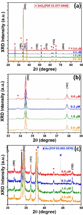
XRD /2 investigations were performed to study the influence of HAuCl4 concentration
on the crystallinity of the Au-NP/ZnO-NW arrays. Figure 2a shows the XRD data in the 10-90° 2 range with a scanning step of 0.02° for Au-NP/ZnO-NW arrays, grown using different concentrations of HAuCl4 (0.0, 0.3, 1.5 and 2.0 μM). Reflections at 31.79º, 34.44º, 36.28º, 47.65º,
56.63º, 62.88º and 72.54º were assigned to the (1 0 0), (0 0 2), (1 0 1), (1 0 2), (1 1 0), (1 0 3) and (0 0 4) planes of wurtzite ZnO (PDF card # 36-1451). While reflections noted with red “*” were
assigned to SnO2 (i.e. to the FTO substrate) according to PDF card # 01-077-0488.24
To study the effect of doping on the crystallinity of the ZnO NWs, the intensity of the (0 0 2) and (1 0 1) reflections was monitored (see Figure 2b). A slight decrease in intensity of the diffraction peaks (0 0 2) and (1 0 1) was observed corresponding to an increase in HAuCl4
concentration up to 2.0 μM. The ionic radii of Au and Zn are r(Au3+) = 0.085 nm and r(Zn2+) =
0.074 nm, respectively.36 Therefore, the Au incorporation in ZnO lattice should lead to an expansion of lattice, shifting the XRD diffraction peaks.36 However, in our case no shift in the
position of the (0 0 2) and (1 0 1) reflections, with the HAuCl4 concentration, was observed (see
Figure 2b). Moreover, additional low intensity peaks were observed for Au-NP/ZnO-NW arrays
at 38.17º and 44.42º, which can be assigned to cubic Au with Fm-3m space group (a = 4.0786 Å, PDF card # 03-065-2870, see Figure 2c).20 The weak reflections of Au indicate that only a small amount of gold on the nanometer scale is present.20 These reflections increase in intensity with
increasing HAuCl4 concentration (see Figure 2c). Therefore, it can be concluded that the Au-NPs
are deposited on the surface of ZnO NWs during the process of electrochemical deposition and that likely no significant doping occurs.14 This could be due to the low solubility of Au in ZnO,9,37
only a few works have reported Au-doped ZnO with evident proof.36,38
Figure 3 shows the results of the TEM analysis of the sample grown using 2.0 μM HAuCl4
at – 0.65 V vs SCE. Figure 3a shows a STEM HAADF image of ZnO microcrystals decorated with Au nanodots which were observed ranging from 10-100 nm in size. An EDX elemental map
9
(Figure 3b) of the area within the red frame correlates the high Z-contrast positions with X-ray signals denoted to the Au M-shell. The electron diffraction pattern depicted in Figure 3c shows the superposition of structural reflections of the ZnO crystal in [211̅̅̅0] orientation, and reflection spots originating from the (1 1 1) and (0 0 2) planes of fcc gold, with d = 0.231 nm and d = 0.201 nm, respectively.39 No systematic orientation relationship between the ZnO and the Au
lattice could be identified. For the Au nanodots, multiple twinning40,41 as well as an amorphous shell coating the nanodot could be evidenced by high-resolution imaging.
3.3. EDX and XPS studies of the AuNP/ ZnO NWs
Analysis by energy dispersive X-ray spectroscopy (EDX) on a Zeiss SEM has been performed to give a rough estimate about the molar Au content in the nanowire arrays prepared in the presence of increasing HAuCl4 concentration. The results are presented in Table S1. The molar
ratio between gold and zinc in the Au-NP/ZnO-NWs increased with the HAuCl4 concentration in
the bath and was comparable with the ratio present in the deposition bath. Two samples of Au-NP/ZnO-NW arrays, grown using the addition of 0.6 and 0.9 µM of HAuCl4 to the ZnO NW
growth solution, were analyzed by using XPS. Figure 4a shows a survey spectrum of a typical Au-NP/ZnO-NW array grown using a solution containing 0.6 µM of HAuCl4. The following
elements were detected: C, O, Zn and Au and the relative atomic concentrations are shown below the spectrum. Generally, the deposition process does not contain carbon and so carbon is not expected to be present in the films. However, since the samples were exposed to the open air and no surface cleaning was performed prior XPS characterization, the carbon observed can be attributed to adventitious carbon resulting from exposure to the ambient atmosphere.42 The presence of the adventitious carbon (285.0 eV) allowed us to use it as a reference for energy calibration. Detailed deconvolution of C-1s spectrum (Figure 4b) shows that in addition to the adventitious carbon there are also two peaks present at 286.7 eV and 289.4 eV, corresponding to CO and CO2, respectively.42
10
Au-NP/ZnO-NW arrays grown using solutions with 0.6 and 0.9 µM of HAuCl4 contain
around 0.4 at% and 0.6 at% of Au, respectively, as revealed by XPS analysis. This is slightly lower in comparison to the data measured using EDX (see Table S1). High resolution XPS spectra of Au-4d are shown in Figure 4c. The peaks observed at 352.26 and 334.72 eV can be attributed to metallic gold and are in a good agreement with the XPS data reported in the literature.43,44 As will be discussed later, samples containing different concentration of gold demonstrate different gas sensing behavior. In Figure 4d, the high resolution spectrum of O-1s core level is depicted. To get more insight into the chemical composition of the sample surface, the high resolution O-1s spectrum was de-convoluted using several components, following the proposed structure suggested in Ref. 45. The resulted fitting is depicted in Figure 4d, and it contains the following three main components: ZnO (530.4 eV), defective ZnOx or Zn(OH)2 (531.5 eV) and OH groups
or adsorbed oxygen (533.2 eV).14,45 Additionally, two smaller peaks located at 531.0 eV and 532.5 eV were attributed to adventitious CO and CO2, respectively.45,46
3.4. Optical properties of the AuNP/ZnO NWs
It was demonstrated that defects in ZnO can greatly affect the gas sensing properties.47,48 In this case, the measurements of optical properties can provide useful information related to defects in ZnO nanowires. Figure 5a shows UV-visible transmission spectra of the AuNP-modified ZnO NWs arrays grown using different concentrations of HAuCl4 in the growth solution.
While unmodified ZnO NW arrays are highly transparent in the near-IR region (close to 100%), by adding the HAuCl4 to the growth solution a decrease in transparency for the entire UV-visible
spectrum can be observed. No shift of the band-edge, corresponding to an increase of HAuCl4
concentration, was observed. The optical band gap (Eg) was obtained from the intercept of (αhν)2
vs. photon energy (hν) (see Figure 5b). It can be observed that no changes in value of Eg (~ 3.26
eV) are induced by an increase in the HAuCl4 concentration. Therefore, no evidence of doping
11
The presence of Au-NPs in the Au-NP/ZnO-NW arrays was further demonstrated by the UV–vis absorption spectra. Figure 5c shows the absorbance spectra of Au-NP/ZnO-NW arrays grown using different concentrations of HAuCl4 in the growth solution. The gradual increase in
the peak intensity at ~ 540 nm with higher concentration of HAuCl4 is observed (see Figure 5c),
which is attributed to the surface plasmon resonance of Au NPs,3,49 demonstrating the successful surface modification of ZnO NWs with Au NPs.
The photoluminescence (PL) spectra measured at room temperature for Au-NP/ZnO-NW arrays, grown using different concentrations of HAuCl4 in the growth solution, is presented in
Figure 5d. No visible emission due to bulk and surface defects is observed, either for the
unmodified ZnO NWs or Au-NP/ZnO-NWs, demonstrating that the synthesized NWs possess high structural quality, even with a deposition temperature of only 90 °C.23 No shift of the near-band-edge (NBE) emission peak was observed, corresponding to an increase in HAuCl4 concentration
(see Figure 5d). However, a gradual increase in intensity of NBE emission with increase in HAuCl4 concentration was observed. The emission is enhanced by Au as the surface is higher,
despite stronger reabsorption at the wavelengths of the ZnO emission. As the absorbance increases with the HAuCl4 concentration as seen in Figure 5c, this unexpected enhancement of the UV
emission may be attributed to the strong interfacial coupling between the metal Au NPs and the semiconductor ZnO NWs as observed in Ref. 49, where Au surface electrons are transferred to the
ZnO nanowires leading to an increase in electron density in the conduction band of ZnO resulting in an increased recombination rate.49
12
From the above discussions, Au-doping in bulk of ZnO NW was not evidenced, however, surface modification of Au-NP/ZnO-NWs was highlighted. To shed light on possible Au/ZnO structures involved, we present data obtained on models of Au-doped bulk ZnO wurtzite and adsorption of Au clusters of different sizes on the clean (undoped) ZnO (10-10) surface, as an example of surface functionalization. As previously performed for the bulk case of Ag23 and Pd,14 calculations have also been performed on: (i) pure ZnO, (ii) doped ZnO with inserted Au (Aui) at
a 1.85 at% doping amount, to gain insight on the effect of the Au insertion into the wurtzite bulk structure on the electronic properties. The unit cell of the inserted Au:ZnO system is shown in
Figure S6 and corresponding band structures are shown in Figure S7, along with obtained data in Table S2.
Computed shortest metal to O distances (d1 to d6 in Table S2) indicate that when Au is
inserted in the ZnO lattice, a highly distorted octahedron around Au can be evidenced, with distances ranging between 2.37 and 3.94 Å. The a and b wurtzite lattice vectors are slightly increased (+0.4%), while the c lattice vector is decreased of about -1.6%. From the data of Figure
S7 and Table S2, it is clear that the ZnO band gap decreases upon insertion of Au, by at least 1.1
eV. Gold mainly contributes through 5d orbitals at the top of the valence band (VB) and at the bottom of the conduction band (CB), with bands possessing very low dispersion, indicating an almost atomic-like character. The lack of a shallow level at the bottom of the CB indicates that no p-type ZnO is obtained however, as already outlined for Pd14 or Ag23 doping.
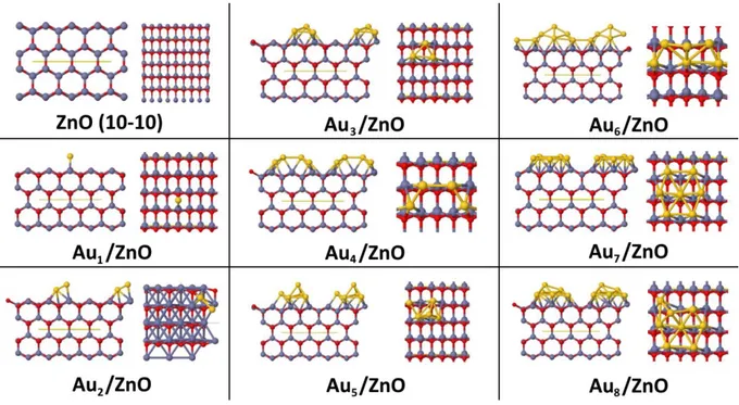
Adsorption of small Aun clusters (n ranging from 1 to 8) on a bulk ZnO (10-10) surface[17, 30] has
also been considered (see Figure 6). Comments on the functionalized surface models can be found in Supporting Information Text S2.
From the data collected in Table S3, Supporting Information, the negative adsorption energies obtained indicate the stable adsorption of the Aun clusters in all the cases investigated,
13
adjacent clusters from one periodic cell to the other. In particular, while Au atoms of small clusters tend to occupy bridge sites between Zn and O surface atoms, in larger clusters, Au atoms tend to occupy hollow sites, with a clear hcp motif obtained for the Au7 and Au8 clusters. In addition,
larger clusters tend to spread on the ZnO substrate, as evidenced by the dAu-Au distances reported
in Table S3, which increase from the smallest to the largest clusters. Both bonding to surface Zn and O atoms can be evidenced, the shortest distances involving surface O atoms. A charge transfer from the Aun cluster to the ZnO substrate can also been evidenced, the Aun cluster being positively
charged, with a charge value close to +1, as already highlighted in the case of the adsorption of Au9/TiO2 (001),50 for instance. Computed band gaps globally decrease upon increasing the size of
the adsorbed Aun cluster, and all reported band gaps are lower than that of the clean ZnO (10-10)
surface (3.88 eV). From Figure S8, Supporting Information, weakly-interacting Au5d levels
contribute mainly to the band gap decrease commented above for the functionalized surface. Shallow levels can be observed in all cases, both at the top of the VB and at the bottom of the CB. Together with the charge transfer mentioned above, this clearly outlines that the NP size strongly influences the ZnO electronic structure, with very different reactivity of the functionalized ZnO substrate possible, depending on the size of the chosen NP.
3.6. Gas nanosensors based on individual Au-NP/ZnO-NWs
The nanosensor devices based on single Au-NP/ZnO-NWs were fabricated following the procedures reported by Lupan et al.15,51 The Au-NP/ZnO-NWs were removed from the NW arrays
grown on the original substrate via sonication in ethanol. In order to obtain a lower density of NWs on the chip for further integration into device the transfer to an intermediate SiO2 (300 nm)-coated
Si substrate (SiO2/Si) was used.14 Next, the dispersion was diluted further to decrease the density
of NWs on the substrate and for further transfer on special designed chip with pre-patterned Au/Cr electrical pads using a direct contact technique and a gentle rubbing few times in order to obtain a
14
low density and good distribution of NWs on the chip. Finally, the NWs were connected to the Au/Cr electrical pads using Pt complex in FIB/SEM by maskless localized patterning feature, forming the Au/Pt/ZnO/Pt/Au structure. The schematic illustration of the device connection is presented in Figure S9. Figure 7a shows the typical image of the device fabricated from an individual Au-NP/ZnO-NW. The Au-NPs can be observed on the ZnO NW surface (see inset from
Figure 7a). The typical current – voltage (I – V) characteristic of device based on an individual
Au-NP/ZnO-NW is presented in Figure 7b. The nonlinear and asymmetrical I – V curves indicate on the formation of double-Schottky contacts which was observed for all samples. The formation of double-Schottky contacts is due to higher work function of Pt (ϕ = 6.1 eV) contacts compared to electron affinity of ZnO NW (Ea = 4.2 eV).14,15 The asymmetry of I – V curves can be a result
of the different contact barriers, different area of contacts and barrier height.11,12,18
Figure S10a shows the gas response to 100 ppm of H2 gas for individual ZnO NWs grown
using different concentrations of HAuCl4. It is necessary to mention that no Au NPs were observed
on the surface of these NWs. Also, for these ZnO NWs the diameter is 120 ± 10 nm in order to investigate only the potential influence of NW growth in different concentrations of HAuCl4. The
results from Figure S10a demonstrate that the concentration of HAuCl4 does not significantly
influence the gas response of individual ZnO NWs. This can be attributed to the fact that the ZnO NWs are not doped with Au, nor show large amounts of structural defects. Therefore we conclude that the main parameter that is important for the improvement of the gas response is the number of Au NPs on the surface of individual NWs, i.e. the surface ratio of nanoscale Schottky contacts to the pristine ZnO surface.
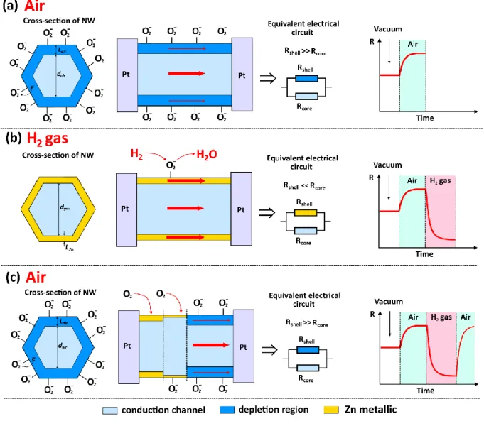
To achieve a considerable increase in gas response by surface-modification of the ZnO NWs with Au NPs, a gas sensing mechanism is proposed, which is attributed to both the electronic and chemical sensitization.52 Figure 8 shows an illustration of the proposed gas sensing mechanism of devices based on individual Au NP-modified ZnO NWs. Under exposure in ambient
15
air at room temperature, the oxygen species are adsorbed on the surface of the ZnO nanowires by capturing free electrons from the conduction band:13,15,52
O2 + e– → O2–(ad) (2)
This reduction results in the formation of a region with higher electrical resistivity than the conductive core at the surface of the ZnO NW (see Figure 8a).13,15 The width of the electron depletion region was noted with Lair, while the diameter of conduction channel was noted as dair
(see Figure 8a). Due to operation at room temperature the chemical sensitization effect, described above, is considerably reduced, i.e. adsorption of more oxygen species occurs via the “spillover effect”, which was observed at high operating temperatures (thermally activated event, > 200 ºC).53
In the case of room temperature conditions, the electronic sensitization is a dominant factor, which can greatly influence the electrical transport through the conduction channel due to formation of nanoscale Schottky barriers at the Au/ZnO interface (see Figure 8a).13,19,22,52 As a result, the formation of Schottky barriers lead to an essential narrowing of the conduction channel (dgas) and
a widening of the electron depletion region (Lgas, see Figure 8a).
Under exposure to H2 gas, the hydrogen molecules are oxidized by the adsorbed oxygen
species as follow:15,54 − − → + + O ad H O e H 12 2 2 2 1 2 ( ) (3)
The released electrons will contribute to the narrowing of the electron depletion region, or a widening of the conduction channel (see Figure 8b). Due to the exothermic nature of the reaction
16
(1.8 kcal mol−1), the water molecules desorbs quickly from the surface.54 In the case of
Au-NP/ZnO-NWs, the modulation of the conduction channel diameter will be larger, which will lead to greater change in current flowing through the conduction channel, resulting in a higher gas response (see Figure 8b).13,15 Therefore, the formation of nanoscale Schottky barriers is an efficient way to highly improve the sensing properties of individual nanostructures such as nanowires. In this respect, works on AuNP/ZnO nanorod structures by Shingange et. al.55 and
Hosseini et.al.56 demonstrate that a narrow size distribution of Au-NPs with diameter between 5-15 nm and a uniform surface coverage yields the highest response at room temperature to H2 or
H2S gas.
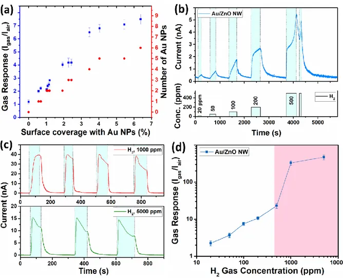
Figure 9a shows the behavior of the measured gas response to 100 ppm of H2 gas for
individual Au-NP/ZnO-NWs, integrated in nanosensors, versus ratio of the Schottky contact area formed by Au NPs on the ZnO to the uncovered ZnO surface. This ratio is further called the “Au NPs surface coverage” and is determined from SEM images. The coverage was calculated by (SNP · 100%)/SNW, where SNP is the Schottky contact area formed by Au-NPs (calculated as πr2,
with r the radius of the Au-NP approximated as half-spheres) on the surface of ZnO NW and SNW
is the surface of ZnO NWs (calculated as 2πrh, where r and h are the radius and length of NW). The gas response was measured at room temperature under 1 V applied bias voltage, in order to reduce the self-heating effect.15 All chosen NWs possess diameters of 120 ± 10 nm, in order to
investigate only the influence of Schottky contact area. As expected, the gas response to hydrogen gas increased with the percentage of the Au covering surface. The number of Au-NPs follows the same tendency as the gas response demonstrating that the surface coverage of the Au-NPs is an essential factor in order to achieve a higher gas response. Further, the H2 gas response for
individual Au-NP/ZnO-NWs with ~ 0.0, ~ 1.1, ~ 2.2, ~ 2.4, ~ 4.0 and ~ 6.4% Au-NPs coverage is 1.2, 2.4, 4.2, 6.8 and 7.5, respectively. The gas response at room temperature to different vapors of volatile organic compounds (VOCs, concentration of 100 ppm) is presented in Figure S10b and S10c. As shown, the gas response to VOC vapors such as ethanol, acetone, 2-propanol,
n-17
butanol and methanol is lower than 1.1, demonstrating high selectivity of Au-NP/ZnO-NWs to hydrogen gas at room temperature. This high selectivity of H2 is also characteristic for unmodified
ZnO NWs,15,54 therefore, no change in selectivity of individual NWs was observed with addition
of Au-NPs, but a considerable increase in gas response was induced (by factor of 6.25). To conclude, it is believed that an even larger increase in the gas response to hydrogen gas could be achieved by larger surface coverage density of smaller Au-NPs and a narrower size distribution, regarding this and previous studies.
Figure 9b shows the gas response of one individual Au-NP/ZnO-NW (0.9 μM HAuCl4
and ~ 6.4% Au-NPs coverage) to different concentrations of H2 gas (from 20 to 500 ppm). The
gas response to 20, 50, 100 and 200 ppm is 2.25, 3.7, 7.5 and 10.6, respectively. Under exposure to relatively higher concentrations of 500 ppm a rapid increase in the current value can be observed. A second short pulse of 500 ppm of H2 gas was applied and the same effect observed
(see Figure 9b). Figure 9c shows the gas response to 1000 ppm and 5000 ppm of H2 gas, which
is ~ 329 and ~ 470, respectively. As can be observed from Figure 9b the stabilization of current during exposure to hydrogen gas is slow, as well as recovery, resulting in a “saw-tooth”-like response which indicates on slow saturation rate and can be attributed to the charge accumulation and slow recovery rate of NW which operates at room temperature.57 The increase and further
decrease in current after introducing in the test chamber of the higher concentrations of hydrogen gas (> 500 ppm, see Figure 9c) can be attributed to the competition of two main mechanism involved in the gas sensing process, namely the surface metallization (which will be further discussed in detail) and the adsorption/desorption of the gas species on the surface of sensor.57
Therefore, the individual Au-NPs/ZnO NW needs time to get a stabilized response after exposure to relatively low or high concentrations of hydrogen gas.
The dependence of the gas response to the concentration of H2 gas is presented in Figure
18
sensing tests of the same sensors. In the gas concentration region of 20 – 200 ppm, the gas response is according to a power law relationship:
2
H p
S , where β = 0.72 is the slope of dependence curve
58,59. In the case of gas concentrations higher than 500 ppm, a considerable increase in response
can be observed. The theoretical detection limit of ~ 1 ppm was estimated using the signal/(noise)2
ratio, as was reported by Dua et al.30
Such a sharp increase in the response for gas concentrations higher than 500 ppm (pink region) can be explained using the semiconductor-to-metal transition of ZnO NW surface, which occurs in the presence of H2 gas molecules.60 The same effect was also observed for ultra-thin CuO
NWs,61 ZnO nanofibers,62,63 and ZnO-SnO2 composite nanofibers.64 In the presence of H2 the
surface of ZnO will take on a metallic character. This is due to the fact that the 4s orbital of Zn in ZnO is occupied by one electron (4s1) and when hydrogen gas adsorbs on the surface this orbital
becomes fully occupied (4s2), causing a metallization of the ZnO on the surface.60,65,66 As shown
in the results, in the presence of H2 gas the hydrogen molecules will adsorb on the surface of the
ZnO NW (H2(ad) → 2H+ + 2e-), and the surface depletion region of ZnO (resulting from the
adsorption of oxygen molecules) will be narrowed and a thin metallic Zn (ϕZn = 4.3 eV) layer will
be formed (Zn (4s1) + e- → Zn (4s2), see Figure 10a and 10b).60 This process will drastically lower
the resistance between the Pt contacts, leading to considerable increase in current of the device (which was observed in Figure 8b). When the H2 gas is evacuated from the test chamber, the
metallic Zn layer will be converted back to ZnO ( 2( ) () ( ) 2
1
s s
g Zn ZnO
O + → ), returning the current
value to its original baseline (see Figure 10c).60
However, it is necessary to mention that surface metallization occur at relatively high temperatures, due to necessity of high energy for reduction of metal oxides.62-64 In our case, the
gas sensing is performed at room temperature by applying a bias voltage of 1 V, in order to reduce the self-heating effect. However, the Joule heating of individual Au-NPs/ZnO NW integrated into device is inevitable due to a high increase in current of device at exposure to high concentrations
19
of hydrogen gas (see Figure 9b). Thus, we believe that the locally generated high temperature at exposure to high concentrations of hydrogen gas is responsible for surface metallization of NW.67
Table S4 lists the results on H2 gas sensing of individual structures of metal oxides and
other materials from literature in order to compare with our results. As can be observed, our results are superior to many of the reported data. Another important factor is fast response and recovery (~ 10 s) at exposure to high concentrations of H2 gas (5000 ppm), which is attributed to the
semiconductor-to-metal surface transition process under H2 and leads to enhanced hydrogen
response at concentrations higher than 500 ppm. This allows for its use in the fabrication of rapid detectors for hydrogen gas leakages. Due to its ease of production and its potential applications, the use of liquid and gaseous hydrogen has been developed in various fields such as hydrogenation processes, petroleum transformation, soldering, cryogenic cooling, or chemical substances production.68 Under normal atmospheric conditions, gaseous hydrogen leakage in the air can lead
to an explosive atmosphere easily ignited for hydrogen concentrations between 4% (lower explosive limit (LEL)) and 74.5% (upper explosive limit UEL) — at room temperature and pressure.68,69 Thus, the fast detection of hydrogen leakage is very important for safety purposes,
and is one of the major safety concerns in different fields due to the small ignition energy of only 0.02 mJ, and large velocity of flame propagation.70
4. CONCLUSIONS
In this work, the one-step electrochemical deposition of AuNP-modified ZnO NWs arrays is reported. The optical, chemical and structural investigations were performed in detail demonstrating high crystallinity of the NWs, and that doping of the NWs with Au does not occur. The growth of Au NPs, with diameters varying from 10 to >100 nm on the surface of ZnO NWs was observed with TEM. Individual Au-NP/ZnO-NWs were integrated into sensor devices showing excellent hydrogen gas sensing properties, i.e. high gas response of ~ 7.5 to 100 ppm at
20
room temperature and excellent selectivity against selected alcohols and ketones. It was observed that higher gas response can be achieved by using the individual Au-NP/ZnO-NWs with a higher coverage of Au NPs on the surface (in the case of NPs the gas response is ~ 7.5). At high concentrations of H2 gas, a considerable increase in gas response was observed, which could be
due to surface metallization of the ZnO NW, resulting in ultra-high responses of 329 and 470 for 1000 and 5000 ppm of H2. Such devices are ideal candidates for detection of hydrogen gas leakages
with ultra-low power consumption and the possibility of room temperature operation. DFT calculations performed on Au-doped ZnO bulk and surface functionalized models support and validate the model proposed based on the experimental findings.
■ ASSOCIATED CONTENT
Supporting Information: First voltammetry cycles recorded on the FTO substrate in the ZnO
electrodeposition solutions with various HAuCl4 concentrations. SEM images of Au-modified
ZnO NWs arrays grown using different concentrations of HAuCl4 in electrolyte solution. SEM images at higher magnification of Au-modified ZnO NWs arrays grown using 0.3 μM of HAuCl4
in electrolyte solution in order to show the presence of NPs on the surface of NWs. Side view of the unit cell of doped ZnO wurtzite from computational studies. Computed band structures, total and orbital-projected density of states of (a) ZnO and (b) Au-doped ZnO bulk systems. Computed band structures, total and projected density of states of pure ZnO (10-10), and Aun/ZnO (10-10) with n ranging from 1 to 8. Schematic illustration of connection of the individual Au-NPs/ZnO NW into device. Gas response of individual ZnO NWs (without Au NPs on the surface) with diameter of 120 ± 10 nm versus concentration of HAuCl4 used for grown of NWs. Computed
lattice parameters (a, b, c in Å, α, β and γ in degrees). Computed adsorption energies per Au atom (Eads, in eV), electronic band gaps (Egapα and Egapβ, in eV) and top of valence band energies (EVBα
21
ZnO (10-10) surface and the different Aun/ZnO (10-10) systems considered. Summary of the
hydrogen gas sensors based on individual structures of metal oxides and other materials.The Supporting Information is available free of charge on the ACS Publications website at http://pubs.acs.org
■ AUTHOR INFORMATION Corresponding Authors
*E-mails: ollu@tf.uni-kiel.de oleg.lupan@mib.utm.md ra@tf.uni-kiel.de thierry.pauporte@chimieparistech.psl.eu
Notes
The authors declare no competing interest.
ACKNOWLEDGMENTS
Dr. Lupan gratefully acknowledges PSL University, Chimie-ParisTech for invited professor position and CNRS Council for support as expert scientist at IRCP Chimie ParisTech, Paris. This research was sponsored partially by the German Research Foundation (DFG- Deutsche Forschungsgemeinschaft) under the schemes SFB1261, FOR2093 and by SFB859. Dr. Lupan acknowledges the Alexander von Humboldt Foundation for the research fellowship for experienced researchers 3-3MOL/1148833 STP at the Institute for Materials Science, Kiel University, Germany. This research was partly supported by the STCU within the Grant 6229. Dr. Ilaria Ciofini, Dr. Frédéric Labat and Jun Su would like to acknowledge the HPC resources of TGCC made available by GENCI (Grand Equipement National de Calcul Intensif) through project A0050810135. Jun Su gratefully acknowledges the China Scholarship Council (Grant number 201706150081) for PhD funding.
22 ■ REFERENCES
(1) Franklin, A. D. Nanomaterials in Transistors: From High-Performance to Thin-Film Applications.
Science 2015, 349, 2750-2751 - 2760-2759.
(2) Mishra, Y. K.; Adelung, R. ZnO Tetrapod Materials for Functional Applications. Mater. Today 2017,
21, 631-651.
(3) Li, P.; Wei, Z.; Wu, T.; Peng, Q.; Li, Y. Au−ZnO Hybrid Nanopyramids and Their Photocatalytic Properties. J. Am. Chem. Soc. 2011, 133, 5660-5663.
(4) Özgür, Ü.; Alivov, Y. I.; Liu, C.; Teke, A.; Reshchikov, M. A.; Doğan, S.; Avrutin, V.; Cho, S. J.; Morkoç, H. A Comprehensive Review of ZnO Materials and Devices. J. Appl. Phys. 2005, 98, 041301. (5) Katoch, A.; Kim, J.-H.; Kim, S. S. TiO2/ZnO Inner/Outer Double-Layer Hollow Fibers for Improved
Detection of Reducing Gases. ACS Appl. Mater. Interfaces 2014, 6, 21494-21499.
(6) Katoch, A.; Kim, J.-H.; Kwon, Y. J.; Kim, H. W.; Kim, S. S. Bifunctional Sensing Mechanism of SnO2– ZnO Composite Nanofibers for Drastically Enhancing the Sensing Behavior in H2 Gas. ACS Appl.
Mater. Interfaces 2015, 7, 11351-11358.
(7) Choi, S.-W.; Katoch, A.; Sun, G.-J.; Kim, J.-H.; Kim, S.-H.; Kim, S. S. Dual Functional Sensing Mechanism in SnO2–ZnO Core–Shell Nanowires. ACS Appl. Mater. Interfaces 2014, 6, 8281-8287. (8) Zhong Lin, W. Zinc Oxide Nanostructures: Growth, Properties and Applications. J. Phys. Cond.
Matter 2004, 16, R829.
(9) Pearton, S. J.; Norton, D. P.; Ip, K.; Heo, Y. W.; Steiner, T. Recent Advances in Processing of ZnO. J.
Vac. Sci. Technol., B 2004, 22, 932-948.
(10) Huang, M. H.; Mao, S.; Feick, H.; Yan, H.; Wu, Y.; Kind, H.; Weber, E.; Russo, R.; Yang, P. Room-Temperature Ultraviolet Nanowire Nanolasers. Science 2001, 292, 1897.
(11) Li, Q. H.; Wan, Q.; Liang, Y. X.; Wang, T. H. Electronic Transport Through Individual ZnO Nanowires.
Appl. Phys. Lett. 2004, 84, 4556-4558.
(12) Li, Q. H.; Liang, Y. X.; Wan, Q.; Wang, T. H. Oxygen Sensing Characteristics of Individual ZnO Nanowire Transistors. Appl. Phys. Lett. 2004, 85, 6389-6391.
(13) Kolmakov, A.; Klenov, D. O.; Lilach, Y.; Stemmer, S.; Moskovits, M. Enhanced Gas Sensing by Individual SnO2 Nanowires and Nanobelts Functionalized with Pd Catalyst Particles. Nano Lett. 2005, 5, 667-673.
(14) Lupan, O.; Postica, V.; Adelung, R.; Labat, F.; Ciofini, I.; Schürmann, U.; Kienle, L.; Chow, L.; Viana, B.; Pauporté, T. Functionalized Pd/ZnO Nanowires for Nanosensors. Phys. Status Solidi (RRL) 2017,
12, 1700321.
(15) Lupan, O.; Cretu, V.; Postica, V.; Ahmadi, M.; Cuenya, B. R.; Chow, L.; Tiginyanu, I.; Viana, B.; Pauporté, T.; Adelung, R. Silver-Doped Zinc Oxide Single Nanowire Multifunctional Nanosensor with a Significant Enhancement in Response. Sens. Actuators B 2016, 223, 893-903.
(16) Lupan, O.; Postica, V.; Gröttrup, J.; Mishra, A. K.; de Leeuw, N. H.; Adelung, R. Enhanced UV and Ethanol Vapour Sensing of a Single 3-D ZnO Tetrapod Alloyed with Fe2O3 Nanoparticles. Sens.
Actuators B 2017, 245, 448-461.
(17) Kuang, Q.; Lao, C.-S.; Li, Z.; Liu, Y.-Z.; Xie, Z.-X.; Zheng, L.-S.; Wang, Z. L. Enhancing the Photon- and Gas-Sensing Properties of a Single SnO2 Nanowire Based Nanodevice by Nanoparticle Surface Functionalization. J. Phys. Chem. C 2008, 112, 11539-11544.
(18) Hu, Y.; Zhou, J.; Yeh, P. H.; Li, Z.; Wei, T. Y.; Wang Zhong, L. Supersensitive, Fast‐Response Nanowire Sensors by Using Schottky Contacts. Adv. Mater. 2010, 22, 3327-3332.
(19) Gogurla, N.; Sinha, A. K.; Santra, S.; Manna, S.; Ray, S. K. Multifunctional Au-ZnO Plasmonic Nanostructures for Enhanced UV Photodetector and Room Temperature NO Sensing Devices. Sci.
Rep. 2014, 4, 6483.
(20) Guo, J.; Zhang, J.; Zhu, M.; Ju, D.; Xu, H.; Cao, B. High-Performance Gas Sensor Based on ZnO Nanowires Functionalized by Au Nanoparticles. Sens. Actuators B 2014, 199, 339-345.
(21) Liu, K.; Sakurai, M.; Liao, M.; Aono, M. Giant Improvement of the Performance of ZnO Nanowire Photodetectors by Au Nanoparticles. J. Phys. Chem. C 2010, 114, 19835-19839.
23
(22) Zheng, Z. Q.; Wang, B.; Yao, J. D.; Yang, G. W. Light-Controlled C2H2 Gas Sensing Based on Au-ZnO Nanowires with Plasmon-Enhanced Sensitivity at Room Temperature. J. Mater. Chem. C 2015, 3, 7067-7074.
(23) Pauporté, T.; Lupan, O.; Zhang, J.; Tugsuz, T.; Ciofini, I.; Labat, F.; Viana, B. Low-Temperature Preparation of Ag-Doped ZnO Nanowire Arrays, DFT Study, and Application to Light-Emitting Diode. ACS Appl. Mater. Interfaces 2015, 7, 11871-11880.
(24) Lupan, O.; Pauporté, T.; Chow, L.; Viana, B.; Pellé, F.; Ono, L. K.; Roldan Cuenya, B.; Heinrich, H. Effects of Annealing on Properties of ZnO Thin Films Prepared by Electrochemical Deposition in Chloride Medium. Appl. Surf. Sci. 2010, 256, 1895-1907.
(25) Lupan, O.; Pauporté, T. Hydrothermal Treatment for the Marked Structural and Optical Quality Improvement of ZnO Nanowire Arrays Deposited on Lightweight Flexible Substrates. J. Cryst.
Growth 2010, 312, 2454-2458.
(26) Pauporté, T.; Bataille, G.; Joulaud, L.; Vermersch, F. J. Well-Aligned ZnO Nanowire Arrays Prepared by Seed-Layer-Free Electrodeposition and Their Cassie−Wenzel Transition after Hydrophobization. J. Phys. Chem. C 2010, 114, 194-202.
(27) Lupan, O.; Chai, G.; Chow, L. Fabrication of ZnO Nanorod-Based Hydrogen Gas Nanosensor.
Microelectron. J. 2007, 38, 1211-1216.
(28) Lupan, O.; Cretu, V.; Deng, M.; Gedamu, D.; Paulowicz, I.; Kaps, S.; Mishra, Y. K.; Polonskyi, O.; Zamponi, C.; Kienle, L.; Trofim, V.; Tiginyanu, I.; Adelung, R. Versatile Growth of Freestanding Orthorhombic α-Molybdenum Trioxide Nano- and Microstructures by Rapid Thermal Processing for Gas Nanosensors. J. Phys. Chem. C 2014, 118, 15068-15078.
(29) Lupan, O.; Postica, V.; Mecklenburg, M.; Schulte, K.; Mishra, Y. K.; Fiedler, B.; Adelung, R. Low Powered, Tunable and Ultra-Light Aerographite Sensor for Climate Relevant Gas Monitoring. J.
Mater. Chem. A 2016, 4, 16723-16730.
(30) Dua, V.; Surwade Sumedh , P.; Ammu, S.; Agnihotra, S. R.; Jain, S.; Roberts Kyle , E.; Park, S.; Ruoff Rodney , S.; Manohar Sanjeev , K. All‐Organic Vapor Sensor Using Inkjet‐Printed Reduced Graphene Oxide. Angew. Chem., Int. Ed. 2010, 49, 2154-2157.
(31) Argoubi, W.; Saadaoui, M.; Ben Aoun, S.; Raouafi, N. Optimized Design of a Nanostructured SPCE-Based Multipurpose Biosensing Platform Formed by Ferrocene-Tethered Electrochemically-Deposited Cauliflower-Shaped Gold Nanoparticles. Beilstein J. Nanotechnol. 2015, 6, 1840-1852. (32) Song, Y.; Ma, Y.; Wang, Y.; Di, J.; Tu, Y. Electrochemical Deposition of Gold–Platinum Alloy
Nanoparticles on an Indium Tin Oxide Electrode and Their Electrocatalytic Applications.
Electrochim. Acta 2010, 55, 4909-4914.
(33) Liang, J. K.; Su, H. L.; Kuo, C. L.; Kao, S. P.; Cui, J. W.; Wu, Y. C.; Huang, J. C. A. Structural, Optical and Electrical Properties of Electrodeposited Sb-Doped ZnO Nanorod Arrays. Electrochim. Acta 2014, 125, 124-132.
(34) Wang, F.; Seo, J.-H.; Li, Z.; Kvit, A. V.; Ma, Z.; Wang, X. Cl-Doped ZnO Nanowires with Metallic Conductivity and Their Application for High-Performance Photoelectrochemical Electrodes. ACS
Appl. Mater. Interfaces 2014, 6, 1288-1293.
(35) Wijnhoven, J. E. G. J.; Zevenhuizen, S. J. M.; Hendriks, M. A.; Vanmaekelbergh, D.; Kelly, J. J.; Vos, W. L. Electrochemical Assembly of Ordered Macropores in Gold. Adv. Mater. 2000, 12, 888-890. (36) Sahu, D.; Panda, N. R.; Acharya, B. S.; Panda, A. K. Enhanced UV Absorbance and
Photoluminescence Properties of Ultrasound Assisted Synthesized Gold Doped ZnO Nanorods.
Optical Mater. 2014, 36, 1402-1407.
(37) Lee, E.-C.; Chang, K. J. Possible p-Type Doping with Group-I Elements in ZnO. Phys. Rev. B 2004,
70, 115210.
(38) Xu, Y.; Yao, B.; Li, Y. F.; Ding, Z. H.; Li, J. C.; Wang, H. Z.; Zhang, Z. Z.; Zhang, L. G.; Zhao, H. F.; Shen, D. Z. Chemical States of Gold Doped in ZnO Films and Its Effect on Electrical and Optical Properties.
J. Alloys Comp. 2014, 585, 479-484.
(39) Morris, M. C.; McMurdie, H. F.; Evans, E. H.; Paretzkin, B.; Degrbot, J. H. Standard X-ray Diffraction Powder Patterns: Section 13-Data for 58 Substances. Interim Report National Bureau of
24
(40) Johnson, C. L.; Snoeck, E.; Ezcurdia, M.; Rodríguez-González, B.; Pastoriza-Santos, I.; Liz-Marzán, L. M.; Hÿtch, M. J. Effects of Elastic Anisotropy on Strain Distributions in Decahedral Gold Nanoparticles. Nat. Mater. 2007, 7, 120.
(41) Seo, D.; Yoo, C. I.; Chung, I. S.; Park, S. M.; Ryu, S.; Song, H. Shape Adjustment between Multiply Twinned and Single-Crystalline Polyhedral Gold Nanocrystals: Decahedra, Icosahedra, and Truncated Tetrahedra. J. Phys. Chem. C 2008, 112, 2469-2475.
(42) Greczynski, G.; Hultman, L. C 1s Peak of Adventitious Carbon Aligns to the Vacuum Level: Dire Consequences for Material's Bonding Assignment by Photoelectron Spectroscopy.
ChemPhysChem 2017, 18, 1507-1512.
(43) Tian, Y.; Tatsuma, T. Mechanisms and Applications of Plasmon-Induced Charge Separation at TiO2 Films Loaded with Gold Nanoparticles. J. Am. Chem. Soc. 2005, 127, 7632-7637.
(44) Moulder, J. F.; Chastain, J. Handbook of X-ray Photoelectron Spectroscopy: A Reference Book of
Standard Spectra for Identification and Interpretation of XPS Data; Physical Electronics Division,
Perkin-Elmer Corporation, 1992.
(45) Lupan, O.; Chow, L.; Ono, L. K.; Cuenya, B. R.; Chai, G.; Khallaf, H.; Park, S.; Schulte, A. Synthesis and Characterization of Ag- or Sb-Doped ZnO Nanorods by a Facile Hydrothermal Route. J. Phys.
Chem. C 2010, 114, 12401-12408.
(46) Armelao, L.; Fabrizio, M.; Gialanella, S.; Zordan, F. Sol–Gel Synthesis and Characterisation of ZnO-Based Nanosystems. Thin Solid Films 2001, 394, 89-95.
(47) Ahn, M. W.; Park, K. S.; Heo, J. H.; Park, J. G.; Kim, D. W.; Choi, K. J.; Lee, J. H.; Hong, S. H. Gas Sensing Properties of Defect-Controlled ZnO-Nanowire Gas Sensor. Appl.Phys. Lett. 2008, 93, 263103.
(48) Li, L. M.; Du, Z. F.; Wang, T. H. Enhanced Sensing Properties of Defect-Controlled ZnO Nanotetrapods Arising from Aluminum Doping. Sens. Actuators B 2010, 147, 165-169.
(49) Wang, X.; Kong, X.; Yu, Y.; Zhang, H. Synthesis and Characterization of Water-Soluble and Bifunctional ZnO−Au Nanocomposites. J. Phys. Chem. C 2007, 111, 3836-3841.
(50) Jiang, Z.-Y.; Zhao, Z.-Y. Density Functional Theory Study on the Metal–Support Interaction Between a Au9 Cluster and an Anatase TiO2(001) Surface. Phys. Chem. Chem. Phys. 2017, 19, 22069-22077.
(51) Lupan, O.; Postica, V.; Marx, J.; Mecklenburg, M.; Mishra, Y. K.; Schulte, K.; Fiedler, B.; Adelung, R. Individual Hollow and Mesoporous Aero-Graphitic Microtube Based Devices for Gas Sensing Applications. Appl. Phys. Lett. 2017, 110, 263109.
(52) Yamazoe, N. New Approaches for Improving Semiconductor Gas Sensors. Sens. Actuators B 1991,
5, 7-19.
(53) Chang, C.-M.; Hon, M.-H.; Leu, I.-C. Outstanding H2 Sensing Performance of Pd Nanoparticle-Decorated ZnO Nanorod Arrays and the Temperature-Dependent Sensing Mechanisms. ACS Appl.
Mater. Interfaces 2013, 5, 135-143.
(54) Lupan, O.; Chow, L.; Pauporté, T.; Ono, L. K.; Roldan Cuenya, B.; Chai, G. Highly Sensitive and Selective Hydrogen Single-Nanowire Nanosensor. Sens. Actuators B 2012, 173, 772-780.
(55) Shingange, K.; Tshabalala, Z. P.; Ntwaeaborwa, O. M.; Motaung, D. E.; Mhlongo, G. H. Highly Selective NH3 Gas Sensor Based on Au Loaded ZnO Nanostructures Prepared Using Microwave-Assisted Method. J. Colloid Interface Sci. 2016, 479, 127-138.
(56) Hosseini, Z. S.; Mortezaali, A.; Iraji zad, A.; Fardindoost, S. Sensitive and Selective Room Temperature H2S Gas Sensor based on Au Sensitized Vertical ZnO Nanorods with Flower-Like Structures. J. Alloys Compd. 2015, 628, 222-229.
(57) Chan, N. Y.; Zhao, M.; Huang, J.; Au, K.; Wong, M. H.; Yao, H. M.; Lu, W.; Chen, Y.; Ong, C. W.; Chan, H. L. W.; Dai, J. Highly Sensitive Gas Sensor by the LaAlO3/SrTiO3 Heterostructure with Pd Nanoparticle Surface Modulation. Adv. Mater. 2014, 26, 5962-5968.
(58) Volanti, D. P.; Felix, A. A.; Orlandi, M. O.; Whitfield, G.; Yang, D.-J.; Longo, E.; Tuller, H. L.; Varela, J. A. The Role of Hierarchical Morphologies in the Superior Gas Sensing Performance of CuO-Based Chemiresistors. Adv. Funct. Mater. 2013, 23, 1759-1766.
25
(59) Choi, Y.-H.; Kim, D.-H.; Hong, S.-H.; Hong, K. S. H2 and C2H5OH Sensing Characteristics of Mesoporous p-Type CuO Films Prepared via a Novel Precursor-Based Ink Solution Route. Sens.
Actuators B 2013, 178, 395-403.
(60) Katoch, A.; Choi, S.-W.; Kim, H. W.; Kim, S. S. Highly Sensitive and Selective H2 Sensing by ZnO Nanofibers and the Underlying Sensing Mechanism. J. Hazard. Mater. 2015, 286, 229-235. (61) Lupan, O.; Postica, V.; Ababii, N.; Hoppe, M.; Cretu, V.; Tiginyanu, I.; Sontea, V.; Pauporté, T.;
Viana, B.; Adelung, R. Influence of CuO Nanostructures Morphology on Hydrogen Gas Sensing Performances. Microelectron. Eng. 2016, 164, 63-70.
(62) Kim, J.-H.; Mirzaei, A.; Woo Kim, H.; Wu, P.; Kim, S. S. Design of Supersensitive and Selective ZnO-Nanofiber-Based Sensors for H2 Gas Sensing by Electron-Beam Irradiation. Sens. Actuators B 2019,
293, 210-223.
(63) Abideen, Z. U.; Kim, H. W.; Kim, S. S. An Ultra-Sensitive Hydrogen Gas Sensor Using Reduced Graphene Oxide-Loaded ZnO Nanofibers. Chem. Commun. 2015, 51, 15418-15421.
(64) Katoch, A.; Abideen, Z. U.; Kim, H. W.; Kim, S. S. Grain-Size-Tuned Highly H2-Selective Chemiresistive Sensors Based on ZnO–SnO2 Composite Nanofibers. ACS Appl. Mater. Interfaces 2016, 8, 2486-2494.
(65) Xu, H.; Fan, W.; Rosa, A. L.; Zhang, R. Q.; Frauenheim, T. Hydrogen and Oxygen Adsorption on ZnO Nanowires: A First-Principles Study. Phys. Rev. B 2009, 79, 073402.
(66) Wang, Y.; Meyer, B.; Yin, X.; Kunat, M.; Langenberg, D.; Traeger, F.; Birkner, A.; Wöll, C. Hydrogen Induced Metallicity on the ZnO {10-10} Surface. Phys. Rev. Lett. 2005, 95, 266104.
(67) Prades, J. D.; Jimenez-Diaz, R.; Hernandez-Ramirez, F.; Barth, S.; Cirera, A.; Romano-Rodriguez, A.; Mathur, S.; Morante, J. R. Ultralow Power Consumption Gas Sensors Based on Self-Heated Individual Nanowires. Appl. Phys. Lett. 2008, 93, 123110.
(68) Bévenot, X.; Trouillet, A.; Veillas, C.; Gagnaire, H.; Clément, M. Hydrogen Leak Detection Using an Optical Fibre Sensor for Aerospace Applications. Sens. Actuators B 2000, 67, 57-67.
(69) Okazaki, S.; Nakagawa, H.; Asakura, S.; Tomiuchi, Y.; Tsuji, N.; Murayama, H.; Washiya, M. Sensing Characteristics of an Optical Fiber Sensor for Hydrogen Leak. Sens. Actuators B 2003, 93, 142-147. (70) Sumida, S.; Okazaki, S.; Asakura, S.; Nakagawa, H.; Murayama, H.; Hasegawa, T. Distributed
26
Figure 1. SEM images of Au-modified ZnO NWs grown using different concentrations of HAuCl4
27
Figure 2. (a) XRD patterns of the Au-modified ZnO NWs arrays grown using different
concentrations of HAuCl4 in the electrolyte. (b) Position of (0 0 2) and (1 0 1) peaks for
Au-modified ZnO NWs arrays. (c) Demonstration of peaks with low relatively intensity which correspond to Au.
28
Figure 3. Structural and chemical analysis with TEM. (a) STEM dark field image of ZnO nano-
and microwires faceted with gold nanodots (samples grown using 2.0 µM of HAuCl4 at – 0.65 V
vs SCE). (b) STEM EDX elemental mapping of the red framed area in (a) depicting Au nanodots on ZnO. (c) Electron diffraction pattern of ZnO in [211̅̅̅0] orientation superimposing with reflections of Au.
29
Figure 4. XPS spectra of Au-NP/ZnO-NW arrays grown using different concentrations of
HAuCl4: (a) survey spectrum for sample grown using 0.6 µM; (b) high resolution of C-1s peak;
(c) high resolution spectra of Au-4d peaks for two samples grown using 0.6 and 0.9 µM; (d) high resolution of O-1s peak.
30
Figure 5. (a) Transmission spectra; (b) plot of (αhν)2 vs. photon energy (hν); (c) absorbance
spectra; and (d) PL spectra at room temperature for Au-modified ZnO NW arrays grown using different concentrations of HAuCl4. In inset is presented the PL spectra for NBE peak.
31
Figure 6. Side and top views of the unit cells of pure ZnO (10-10) surface with 8 layers, and of
Aun/ZnO (10-10), with n ranging from 1 to 8. Red, grey and yellow balls correspond to O, Zn and
32
Figure 7. (a) Typical SEM image of device based on individual Au-NP/ZnO-NW. In inset is
presented zoomed region with Au NPs attached on the surface of NW. (b) Room temperature current – voltage characteristic of device.
33
Figure 8. Tentatively proposed gas sensing mechanism for individual ZnO and Au-NP/ZnO-NW:
34
Figure 9. (a) Measured gas response versus the Au NPs surface coverage of individual
Au-NP/ZnO-NW (with diameter of 120 ± 10 nm and grown in various solutions of HAuCl4) calculated
from SEM images. The number of Au NPs for each individual Au-NP/ZnO-NW is also presented to show the minor influence of the shear amount of Au NPs on the gas response. (b) The dynamic gas response to different concentrations of H2 gas, (c) the multiple exposures to 1000 and 5000
ppm of H2 gas and (d) the dependence of gas response on H2 gas concentrations for individual
Au-NP/ZnO-NW (with ~ 6.4 % AuNPs coverage). The errors bars represent the standard deviation between the three measurements in the gas sensing testing of the same sensors.
35
Figure 10. Tentatively proposed gas sensing mechanism involving surface metallization for
individual ZnO NW: (a) under exposure in ambient air; (b) under exposure in H2 gas with surface
metallization; (c) under exposure in ambient air with oxidation of metallic Zn and formation of surface depletion region.
36