HAL Id: hal-01104069
https://hal.archives-ouvertes.fr/hal-01104069
Submitted on 11 May 2020
HAL is a multi-disciplinary open access
archive for the deposit and dissemination of
sci-entific research documents, whether they are
pub-lished or not. The documents may come from
teaching and research institutions in France or
abroad, or from public or private research centers.
L’archive ouverte pluridisciplinaire HAL, est
destinée au dépôt et à la diffusion de documents
scientifiques de niveau recherche, publiés ou non,
émanant des établissements d’enseignement et de
recherche français ou étrangers, des laboratoires
publics ou privés.
Fault-aware configurable logic block for reliable
reconfigurable FPGAs
Chagun Basha Basheer Ahmed, Sébastien Pillement, Stanislaw Piestrak
To cite this version:
Chagun Basha Basheer Ahmed, Sébastien Pillement, Stanislaw Piestrak. Fault-aware configurable
logic block for reliable reconfigurable FPGAs. IEEE International Symposium on Circuits & Systems,
May 2015, Lisbonne, Portugal. pp.2732-2735, �10.1109/iscas.2015.7169251�. �hal-01104069�
Fault-aware Configurable Logic Block for Reliable
Reconfigurable FPGAs
B. Chagun Basha
IRISA, Universit´e de Rennes 1, France [email protected]
Sebastien Pillement
IETR, L’UNAM University, France [email protected]
Stanisław J. Piestrak
IJL/Universit´e de Lorraine, France [email protected]
Abstract—Field Programmable Gate Arrays (FPGAs) used in mission-critical applications such as aerospace, nuclear, and defense require high reliability in spite of internal faults. Fortu-nately, today’s FPGAs have the ability to dynamically reconfigure themselves in the field, which may help to mitigate the effects of certain faults affecting the FPGA devices. Although the reconfig-uration process can remove only the upsets affecting the configu-ration bitstream, unfortunately, there are other sources of faults that might directly affect hardware resources of reconfigurable FPGAs. Their nature and consequences differ from those which occur in the configuration bitstream and their effects cannot be corrected by performing configuration writeback. This paper proposes a fault-aware configurable logic block architecture to detect such faults in FPGA-implemented logic circuits. The fault coverage of the proposed architecture is also discussed. Hardware complexity estimations suggest higher efficiency of the approach proposed over similar existing ones.
I. INTRODUCTION
Static Random Access Memory (SRAM) based FPGAs are widely used in many application domains due to their compelling advantages such as high density functionality, run-time partial reconfiguration, and the ability to update the functionality remotely. The most common contemporary FPGA architectures are built of computational logic blocks that include resources to perform combinational and/or sequential functions which are configurable, according to the end ap-plication. Basically, all architectures of reconfigurable FPGA devices use three primitive elements: (i) configurable memory elements (e.g. SRAM cells), (ii) combinational circuit elements (e.g. multiplexers), and (iii) sequential circuit elements (e.g. D flip-flops as user data memory cells). In high reliability applications, an extra care needs to be taken to deal with the occurrence of faults in all of them. Faults may have varying consequences on the hardware architecture, depending on a primitive element affected. Various sources of faults that occur in FPGA devices include process variability, radiation induced Single Event Effects (SEEs), and aging factors.
The goal of this paper is to present a new fault-aware Configurable Logic Block (CLB) architecture which is capable of on-line detection (i.e. during normal functioning) of faults at the fine granular level (i.e. Look-Up Table (LUT) level). The approach proposed relies on identifying combinational and sequential circuit faults separately, which helps in finding a fault and its handling according to its nature. This paper is organized as follows. Section II presents related work whereas Section III describes the consequences of fault occurrence in primitive elements of reconfigurable FPGAs. Section IV details the proposed fault-aware CLB architecture and discusses its
fault coverage. Section V compares the hardware overhead of the proposed architecture with the state-of-the-art approaches. Finally, Section VI concludes the paper.
II. RELATEDWORK
The configuration SRAM can be affected by strikes of high energy particles resulting in bit flips (0 → 1 or 1 → 0), called Single Event Upsets (SEU), which, depending on multiplicity of affected bits, are called Single-Bit Upsets (SBUs) and Multi-Bit Upsets (MBUs). Scrubbing (e.g. configuration writeback) and partial reconfiguration-based approaches can clear only the upsets created in the configuration bitstream [1]. Apart from SEUs, there are other sources of faults that might directly affect the hardware resources present in FPGAs and which cannot be corrected by scrubbing. The nature of such faults and their consequences differ from those which occur in the configura-tion bitstream. To deal with faults which occur in logic circuits, the most commonly used methods rely on functional hardware replication, like Duplication With Comparison (DWC) and Triple Modular Redundancy (TMR) with majority voting (in particular, Xilinx’s XTMR (Xilinx TMR) with majority as well as minority voting [2]). Because these schemes replicate the whole functional hardware unit, one of their drawbacks is that fault detection/identification is done only at the output of the replicated functional block, i.e., at the output of the comparator (in case of DWC) or the voter (in case of TMR). Unfortunately, unless special care is taken, either of these techniques may suffer because of the possibility that the error propagates from its origin, which can result in accumulation of errors inside redundant modules or at the comparator/voter.
As for multiplexers, they cannot be directly affected by radiation-induced SEUs which could cause SBUs and/or MBUs, because they do not contain any storage elements. Nevertheless, as any other combinational circuits, they can be affected by radiation-induced temporary faults called Single Event Transients (SETs). (Although they can also be affected by permanent faults like stuck-at-faults and transistor bridging faults [3], [4], they are significantly less likely and hence will not be considered here explicitly.) Temporary faults can be detected by implementing circuits as self-checking which are capable of signaling error occurrence during normal function-ing of a system [5]. The authors of [7] have developed self-checking logic circuits intended specifically to protect CLBs of FPGAs by adapting the self-checking 2-rail checker circuit proposed in [5]. However, the self-checking version of the CLB proposed in [7] has limited fault coverage, because it incorporates fault checker only at the final level of the
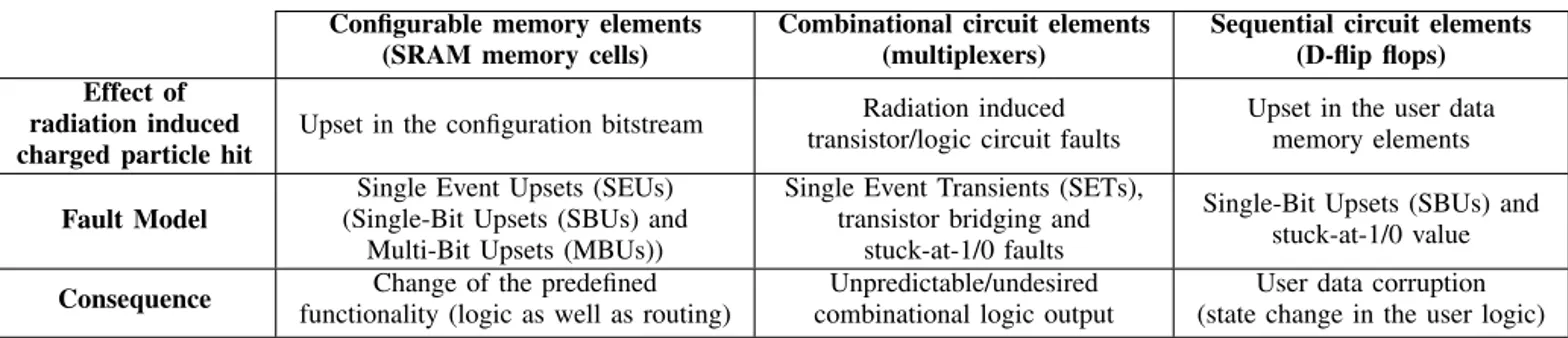
multi-TABLE I: Summary of impact of radiation induced faults on primitive elements of a reconfigurable FPGA
Configurable memory elements (SRAM memory cells)
Combinational circuit elements (multiplexers)
Sequential circuit elements (D-flip flops) Effect of
radiation induced charged particle hit
Upset in the configuration bitstream Radiation induced transistor/logic circuit faults
Upset in the user data memory elements Fault Model
Single Event Upsets (SEUs) (Single-Bit Upsets (SBUs) and
Multi-Bit Upsets (MBUs))
Single Event Transients (SETs), transistor bridging and
stuck-at-1/0 faults
Single-Bit Upsets (SBUs) and stuck-at-1/0 value Consequence Change of the predefined
functionality (logic as well as routing)
Unpredictable/undesired combinational logic output
User data corruption (state change in the user logic)
plexer circuit. This limitation motivated us to propose a new fault-aware CLB architecture, which will have the advantage of detecting faults at a very fine granular level. The scope of this paper is limited to fault detection in combinational as well as sequential circuit elements of a CLB, hence it does not address the configuration bitstream protection.
III. FAULTOCCURRENCE INRECONFIGURABLEFPGAS
Table I summarizes the effects of radiation induced faults in the basic primitive elements of the FPGA architecture. Faults affecting the configuration bitstream could cause soft errors such as SBUs or MBUs which could result in changing the pre-programmed functionality of hardware by affecting routing or logic (CLBs). The configuration bitstream could be protected against errors using scrubbing or built-in error detecting and/or correcting codes. Thanks to run-time background readback and writeback provision available in the recent FPGAs, cleaning the configuration upsets can be done with the help of partial reconfiguration, without halting the entire system. Some Xilinx FPGA devices use Cyclic Redundancy Check (CRC) codes to detect and Hamming Single Error Correcting/Double Error Detecting (SEC/DED) codes to handle errors at the frame level of the configuration bitstream [1].
Some basic combinational and sequential circuit elements are combined together to form a CLB in any FPGA archi-tecture. However, the nature of faults and their consequences differ for each of them. The faults of combinational circuits (which have no memory elements) include SETs and transistor level permanent faults such as bridging, stuck-at-0 or 1 faults. Obviously, these faults result in completely different behavior of a circuit than SEUs affecting the configuration or the user data memory. The most commonly used user-data memory element in FPGA architecture is a D Flip-Flop (D-FF), which is used in CLBs to implement sequential circuitry. A fault in a D-FF could be in the form of user-data memory upset or any other circuit/transistor fault. That is why different fault detection schemes must be used for combinational and sequential circuit elements. A fault in D-FF might change the state of the user logic, which can eventually result in user data corruption.
IV. FAULT-AWARECLB
Fig. 1 shows the block diagram of the proposed fault-aware CLB. The n-input logic block comprises conventionally available combinational and sequential logic elements: a n : 1 LUT, a pair of D-FFs, and the 2 : 1 multiplexer (to choose
between combinational and sequential data output). In the proposed CLB, these three basic functional units are imple-mented as self-checking by using 2-rail codes for multiplexers (similarly e.g. to [7], [8]) and the DWC to protect the D-FF. As for sequential logic resources, these utilize‘Redundant Logic Comparison’ (Logic comparator in Fig. 1) method to detect the user-data upsets as well as the circuit’s internal faults. The discussion concluding this section will reveal the efficiency of the proposed architecture in terms of area overhead and fault coverage when compared to the scheme proposed in [7], as well as DWC- and TMR-based schemes.
Fig. 1: Block diagram of the proposed fault-aware CLB.
Fault-aware Sequential Logic: The D-FFs are widely used in FPGAs to realize the implement sequential functions. There are two types of faults that could affect the normal operation of D-FF in the logic cell:
1) a fault in the D-FF itself, and 2) a flip in the user data (SBU).
As D-FFs are storage elements, it is not possible to adapt self-checking circuit as in multiplexer checking, as it can deal only with circuit faults, not with bit upsets. The contents of D-FFs is updated during computation, hence the user data bits cannot be protected using any of the built-in configuration protection schemes. To deal with circuit faults as well as with user data upsets, some redundancy technique must be adapted. A simple duplication of D-FF with output comparison suffices to identify/detect the fault. Hence, we will take advantage that the ratio between the quantity of basic combinational and sequential logic resources (e.g. LUTs and D-FFs, respectively) could be often like 1 : 2 (for example, a standard CLB
Fig. 2: Transistor scheme of the self-checking 4 : 1 multiplexer of [7].
Fig. 3: Self-checking 24: 1 multiplexer
slice of Xilinx 7 Series architecture consists of 4 LUTs and 8 D-FFs [11]). Also, in [11] was reported that the number of unused flip-flops is high in most of applications. Hence, unused flip-flops of the logic block can be utilized to detect faults in sequential elements by performing duplication with comparison, as it is shown in Fig. 1. The comparator is nothing else but the 2-input XOR gate. In the presence of a fault causing an error, once the mismatch is detected on the outputs of duplicated D-FFs, the comparator generates ‘Err seq’ signal to indicate the presence of error in the sequential logic. The cost of this strategy is an additional XOR gate for each pair of D-FFs and associated routing wires inside the cell.
Fault-aware Combinational Logic: A LUT-based logic block structure is used in the scheme proposed here (similarly to Xilinx Virtex FPGA architectures), due to the possibility of implementing all the n-input of logic functions in it, compared to multiplexer-based architectures. However, the proposed approach can be also adapted to multiplexer-based logic blocks, (such as Microsemi’s FPGA architectures [6]), with less transistor overhead but limited functional efficiency. The configuration data of LUT SRAM cells are part of FPGA’s configuration bitstream and they can be protected using con-figuration bitstream protection scheme such as discussed in [12] and the references therein. Hence, we concentrate here on dealing with faults occurring in the selection multiplexers of the logic block. Before applying any fault mitigation schemes to any given logic resource, it is crucial to understand the fault models and the consequences of their occurrence.
The self-checking 2 : 1 multiplexer built using four transmission gates and an inverter can be found in [8]. Fig. 2 shows a pass-transistor scheme of a self-checking 4 : 1 multiplexer protected using 2-rail code, used in [7]. The transistor pairs (Q17/Q18 and Q19/Q20) used in the checker are characterized by different aspect ratios to achieve different voltage thresholds VT 1and VT 2. It can be achieved in CMOS
technology by various methods as discussed in [9], [11]. If the ‘OUT’ node has an intermediate voltage, the checker outputs E1 and E2 with different voltage levels, otherwise, E1 and E2 have the same voltage level. Indeed, the ‘OUT’ node has
an intermediate voltage when there is a fault in the circuit. Hence, it is interpreted as in the absence of a fault, the output of the checker (E1 E2) assumes the value (11) or (00). If a fault occurs in the multiplexer, (E1 E2) shall assume either (01) or (10). According to (E1 E2), the comparator (i.e. the 2-input XOR) generates the error status signal ‘Err comp’ to indicate the occurrence of a fault in the combinational logic.
The self-checking 4 : 1 multiplexer of Fig. 2 is the basic circuit for the proposed combinational logic protection scheme. The 4 : 1 multiplexer has two functional logic levels 22 and 21 connected to the final 2-rail checker. The LUT selection
multiplexers of the 4-input, 6-input, and 8-input CLBs are constructed by introducing the 2-rail checker circuitry after every second functional logic level of the multiplexer; i.e., larger self-checking multiplexers are constructed using the set of 4 : 1 self-checking multiplexers by connecting them appro-priately. For example, the 24 : 1 self-checking multiplexer is constructed using five 4 : 1 multiplexers using 2-rail checker circuitry at two logic levels 21 and 23, as shown in Fig. 3. The ‘Err seq’ and ‘Err comp’ signals could be used to trigger the appropriate fault mitigation strategy, according to the nature of the fault. Performing task re-execution might clear the user-data upset in D-FF and SETs in combinational circuits in the next operation cycle. If an error persists, it is considered a permanent fault, hence to avoid using faulty resources, task relocation has to be done.
Fault Coverage: The proposed architecture applies self-checking at the fine granular level (circuit level fault detection). Also, it applies different fault detection techniques to combina-tional and sequential logic, according to their fault models and consequences. Hence the proposed scheme is able to detect and identify combinational faults and sequential faults individually. Additionally, in combinational logic, the 2-pair 2-rail checker is used at every second logic level of the multiplexer, which increases the fault coverage of the proposed circuitry. For example, the 4-input logic block is composed of the 24 × 1 LUT SRAM and the 24:1 selection multiplexer. Thus, the
16 : 1 multiplexer has four logic levels subsequently with 24,
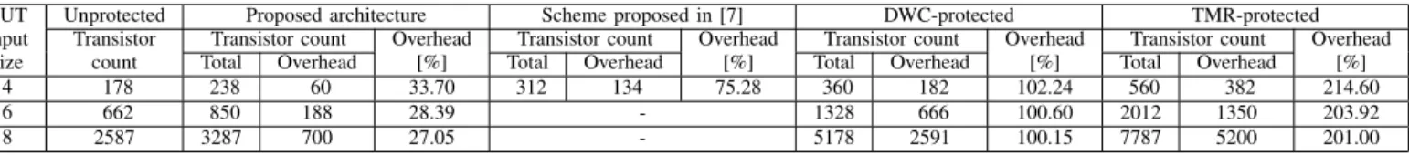
TABLE II: Comparison of hardware overhead of fault-aware CLBs
LUT Unprotected Proposed architecture Scheme proposed in [7] DWC-protected TMR-protected input Transistor Transistor count Overhead Transistor count Overhead Transistor count Overhead Transistor count Overhead
size count Total Overhead [%] Total Overhead [%] Total Overhead [%] Total Overhead [%] 4 178 238 60 33.70 312 134 75.28 360 182 102.24 560 382 214.60 6 662 850 188 28.39 - 1328 666 100.60 2012 1350 203.92 8 2587 3287 700 27.05 - 5178 2591 100.15 7787 5200 201.00
levels numbered 23 = 8 and 21 = 2 to detect the presence of faults (see Fig. 3). The proposed scheme has smaller error latency because, unlike redundancy based techniques such as DWC and TMR, it does not have to wait till the signal reaches the module outputs, so that a comparator or a voter can handle errors; thus it helps to avoid accumulation of errors and enables faster fault detection. As compared to the self-checking scheme of [7], the proposed self-checking combinational circuit has the ability to detect faults at the fine granular level, as it incorporates the 2-rail checker circuitry not just at the last logic level (21) of the multiplexer.
V. HARDWAREOVERHEADCOMPARISON
Table III shows the transistor count for the individual mod-ules used, which helps to estimate the total amount of hardware used. Table II shows hardware complexity estimations which allow to compare the proposed fault-aware CLB against its unprotected version as well as its two fault-aware counterparts: DWC-based and TMR-based. The evaluation is performed for three logic block sizes: 4-input (24 × 1 SRAM and 24 : 1
MUX), 6-input (26 × 1 SRAM and 26 : 1 MUX), and
8-input (28× 1 SRAM and 28: 1 MUX). Digikey’s ’P artSim’
and ’Circuitlab’ workbench tools were used to perform the evaluation of different schemes.
TABLE III: Transistor count of modules used
Module Name Transistor Count SRAM cell of LUT 6T 2-pair 2-rail checker
+ Error evaluator 8T D flip-flop 8T XOR/Comparator 4T 2 : 1 multiplexer 6T
The hardware complexity figures of Table II clearly show that the proposed architecture is significantly more hardware efficient compared to DWC and TMR based schemes which require respectively about three and six times extra hardware than the proposed architecture. For example, to implement the 6-input CLB with proposed fault checking mechanism, only extra 188 transistors are required i.e., 28.39 %, whereas, in case of DWC and TMR the overhead reaches 100.60 % and 203.92 %, respectively. Compared to the 4-input self-checking CLB of [7] which requires a total of 312 transistors, our scheme requires only 238 transistors, i.e. 23.71% less overhead.
VI. CONCLUSION
A new fault-aware configurable logic block (CLB) archi-tecture intended for FPGAs is presented. The novelty lies in
the idea of applying different fault identification mechanism for combinational and sequential logic elements. Evaluation results show that the proposed scheme has less transistor over-head than other known schemes. In particular, it is about three and six times smaller than for schemes based on duplication with comparison and triple modular redundancy. Separate iden-tification of combinational and sequential circuit faults would help in formulating appropriate fault tolerance/mitigation strat-egy in the future.
ACKNOWLEDGMENT
The authors would like to thank the French National Research Agency (ANR) for the research support provided to the ARDyT project (ANR-11-INSE-015).
REFERENCES
[1] C. Carmichael and C. W. Tseng, “Correcting single-event upsets in Virtex-4 FPGA configuration memory,” Xilinx Appl. Note XAPP1088 (v1.0), 5 Oct. 2009.
[2] B. Bridgford, C. Carmichael and C. W. Tseng, “Single-event upset mitigation selection guide,” Xilinx Appl. Note XAPP987 (v1.0), 18 March 2008.
[3] R. F. DeMara and K. Zhang, “Autonomous FPGA fault handling through competitive runtime reconfiguration ,” in Proc. NASA/DoD Conf. Evolv-able Hardware (EH05), pp. 109–116, June 2005.
[4] J.-M. Lauenstein et al., “Single event gate rupture in power MOSFETs: A new radiation hardness assurance approach,” Ph.D Thesis, Univ. Maryland, College Park, MA, USA, 2011.
[5] P. K. Lala, “Self-Checking and Fault-Tolerant Digital Design,” Morgan Kaufmann Publ., San Francisco, CA, USA, 2001.
[6] “Accelerator Series FPGAs - ACT 3 Family”, Microsemi corporation application note : Revision 3, Jan 2012.
[7] S. Pontarelli, G. C. Cardarilli, A. Leandri, M. Ottavi, and A. Salsano, ”A self-checking cell logic block for fault tolerant FPGAs,” in Proc. IEEE Int. Symp. Circuits and Systems (ISCAS), vol. 4, 2002, pp. 477–480. [8] D. P. Vasudevan, P. K. Lala, and J. P. Parkerson, “Self-checking
carry-select adder design based on two-rail encoding,” IEEE Trans. Circuits and Systems—I, Reg. Pap., vol. 54, no. 12, pp. 2696–2705, Dec. 2007. [9] A. Fariborz, B. Kerry, M.J. Hargrove, N.J. Rohrer, and S. Peter, “SOI
CMOS dynamic circuits having threshold voltage control,” US patent number 6433587 B1, Aug, 2002.
[10] N. Mehta, and B. Amrutur, “Dynamic Supply and Threshold Voltage Scaling for CMOS Digital Circuits Using In-situ Power Monitor,” IEEE Trans. VLSI Systems, vol. 20, no. 5, pp. 892–901, May 2012. [11] N. Mehta, Xilinx 7 Series FPGAs: The logical advantage, Xilinx, White
Paper WP405 (v1.0), 6 March 2012.
[12] B. Chagun Basha, S. J. Piestrak, and S. Pillement, “Built-in 3-dimensional Hamming multiple-error correcting scheme to mitigate radiation effects in SRAM-based FPGAs,” in Proc. 10th Int. Symp. on Applied Reconfigurable Computing (ARC), Lect. Notes on Comput. Sci., vol. 8405, pp. 254–261, Jan. 2014.
![Fig. 2: Transistor scheme of the self-checking 4 : 1 multiplexer of [7].](https://thumb-eu.123doks.com/thumbv2/123doknet/8174914.274440/4.903.78.877.121.409/fig-transistor-scheme-self-checking-multiplexer.webp)