BIAS-ENHANCED TUNGSTEN OXIDE FILMS FOR DURABLE ELECTROCHROMIC DEVICES
FRANCIS BLANCHARD
DÉPARTEMENT DE GÉNIE PHYSIQUE ÉCOLE POLYTECHNIQUE DE MONTRÉAL
MÉMOIRE PRÉSENTÉ EN VUE DE L’OBTENTION DU DIPLÔME DE MAÎTRISE ÈS SCIENCES APPLIQUÉES
(GÉNIE PHYSIQUE) MAI 2018
UNIVERSITÉ DE MONTRÉAL
ÉCOLE POLYTECHNIQUE DE MONTRÉAL
Ce mémoire intitulé :
BIAS-ENHANCED TUNGSTEN OXIDE FILMS FOR DURABLE ELECTROCHROMIC DEVICES
présenté par : BLANCHARD Francis
en vue de l’obtention du diplôme de : Maîtrise ès sciences appliquées a été dûment accepté par le jury d’examen constitué de :
M. MOUTANABBIR Oussama, Ph. D., président
M. MARTINU Ludvik, Ph. D., membre et directeur de recherche
Mme KLEMBERG-SAPIEHA Jolanta-Ewa, Doctorat., membre et codirectrice de recherche M. SCHIETTEKATTE François, Ph. D., membre externe
ACKNOWLEDGEMENTS
I first want to thank my research director, Ludvik Martinu, and codirector, Jolanta-Ewa Sapieha, for my time at the FCSEL, both as an undergraduate and master’s student, and all the opportunities that came with it.
I also wish to thank Bill Baloukas who, more than anyone else, has provided guidance and counsel of the utmost quality, along with many discussions. Similarly, Simon Loquai has also always been the right person to ask a question about anything.
Thank you also to all the members, past and present, that made the FCSEL a friendly and stimulating work environment.
One cannot forget to thank the technicians present throughout my time as a student, Francis Turcot and Sébastien Chénard, without whom no work could be done as the systems would inevitably break down in time.
RÉSUMÉ
La technologie des couches minces fait partie intégrante de la vie courante mais reste tout de même largement méconnue du publique. Elle consiste à déposer des couches très minces de matériaux, de l’ordre du micron ou même du nanomètre sur un objet afin de modifier les propriétés et par le fait même, la façon dont il interagit avec le monde. Ces revêtements fonctionnels sont utilisés pour augmenter la durée de vie des outils et engins mécaniques, pour donner de la couleur et brillance à une surface, pour prévenir les égratignures et les reflets sur les lunettes, ainsi qu’une multitude d’autres applications. Un autre usage très important est pour les fenêtres écoénergétiques, où des revêtements spécialement conçus peuvent aider au contrôle de la température en modifiant leur efficacité thermique. Parmi les nanotechnologies dites “vertes” pour la fenestration existe la fenêtre intelligente, basée sur des matériaux électrochromiques ayant la capacité de moduler leur coloration par l’insertion d’ions lorsqu’un courant électrique est appliqué. En cyclant entre un état coloré et un état transparent, l’absorption thermique de la fenêtre peut être ajustée de manière à réduire la consommation énergétique pour le chauffage et la climatisation.
Ce projet s’intéresse principalement au plus connu des matériaux électrochromiques pour ses capacités supérieures: le WO3. Puisque le WO3 et les dispositifs électrochromiques en général ont tendance à souffrir de dégradation lors de longues périodes d’utilisation, l’objectif de ce projet est d’améliorer la durabilité du matériau en modifiant sa microstructure. Pour ce faire, nous avons préparé ce matériau par pulvérisation magnétron RF avec l’assistance d’un bombardement ionique à haute énergie généré par un potentiel électrique appliqué sur le porte-substrat.
Des échantillons ont été préparés avec et sans bombardement ionique, à haute et basse pression, puis ont été analysés par ellipsométrie, spectrophotométrie, microscopie à force atomique, microscopie électronique à balayage, microscopie électronique en transmission et voltammétrie cyclique. Ceci nous a permis d’établir qu’à des énergies assez élevées, le bombardement ionique cause des modifications structurelles importantes, particulièrement de la nanocristallisation et une porosité microstructurale. Pour des échantillons préparés à basse pression, ces changements sont jugés responsables d’une large augmentation de la durabilité par rapport aux échantillons à haute pression, tout en maintenant une structure poreuse favorable pour l’insertion d’ions et la coloration. Des travaux ont aussi été réalisés pour développer de petits dispositifs électrochromiques pour des applications d’authentification de documents importants. Des travaux futurs envisagés en lien avec
ce projet incluent une recherche approfondie sur le mécanisme de croissance du WO3 et d’autres matériaux soumis à un bombardement ionique à haute intensité, ainsi que l’intégration du WO3 modifié par bombardement ionique dans des dispositifs de sécurité.
ABSTRACT
Thin film technology is a critical component of many objects in our daily lives, yet remains mostly unknown to the public at large. It consists in the deposition of very thin layers of material on substrates at the micron or even at the nanometer scale to modify their properties and consequently, the way they interact with the world. These so-called functional coatings can be used to vastly augment the lifetime of tools and mechanical parts, to give color and sheen to a surface, to prevent scratches and glare on glasses as well as multitude other uses. One very important application is for eco-energetic windows, where specially designed coatings can help with temperature control by improving their thermal efficiency. Amongst these “green” nanotechnologies for fenestration is the smart window, based on electrochromic materials which possess the ability of transmission modulation following the application of an electrical current resulting in ion insertion. By switching between a colored and a bleached state, the thermal absorption of the window can be adjusted to reduce the energy required to heat or cool a building.
This work focuses mostly on the most famous electrochromic material for its superior properties: WO3. Since WO3 and electrochromic devices in general tend to suffer from degradation issues over repeated coloration/bleaching cycles, the aim was to improve the durability of the material by changing its microstructure. To do so, we prepared the material with RF magnetron sputtering and the assistance of a high energy ion bombardment generated by substrate biasing.
Samples were prepared at high and low pressures with and without ion bombardment and subsequently analyzed by ellipsometry, spectrophotometry, atomic force microscopy, scanning electron microscopy, transmission electron microscopy and cyclic voltammetry. This allowed us to establish that at high enough energies, the ion bombardment results in significant structural changes, most notably nanocrystallization and microstructural porosity. For samples prepared at low pressures, these changes are thought to be responsible for a large increase in durability over samples deposited at higher pressures whilst maintaining a porous microstructure favorable for ion insertion and coloration. Work was also done towards developing smaller electrochromic devices aimed towards the anticounterfeiting market. Future work based on this project includes further research into the growth mechanisms of WO3 and other materials under high energy ion bombardment as well as integration of the biased WO3 layers into security devices.
TABLE OF CONTENTS
ACKNOWLEDGEMENTS ... iii
RÉSUMÉ ... iv
ABSTRACT ... vi
TABLE OF CONTENTS ... vii
LIST OF TABLES ... x
LIST OF FIGURES ... xi
LIST OF SYMBOLS AND ABBREVIATIONS... xiv
LIST OF APPENDICES ... xvii
CHAPTER 1 : INTRODUCTION ... 1
1.1 Energy consumption and control – smart windows ... 1
1.2 Context of the research ... 5
1.3 Objectives ... 7
1.4 Scientific publications ... 7
1.5 Thesis outline ... 8
CHAPTER 2 : LITERATURE REVIEW AND THEORETICAL BACKGROUND ... 10
2.1 Foreword ... 10 2.2 Electrochromism ... 11 2.2.1 Historical background ... 11 2.2.2 Electrochromic materials ... 12 2.2.3 Coloration mechanism ... 13 2.2.4 Electrochromic devices ... 15
2.3 Fabrication methods ... 22
2.3.1 Electron-beam evaporation ... 22
2.3.2 Sol-gel ... 24
2.3.3 Sputtering ... 25
CHAPTER 3 : METHODOLOGY ... 33
3.1 Bias assisted RF magnetron sputtering ... 33
3.2 Optical properties characterization ... 34
3.2.1 Spectroscopic ellipsometry ... 35 3.2.2 Spectrophotometry ... 36 3.3 Electrochemical characterization ... 37 3.3.1 Cyclic voltammetry ... 37 3.3.2 In situ transmission ... 40 3.4 Physical characterization ... 40
3.4.1 Atomic force microscopy ... 41
3.4.2 Raman spectroscopy ... 41
3.4.3 Rutherford back-scattering ... 42
3.4.4 Scanning electron microscopy ... 43
3.4.5 Transmission electron microscopy ... 44
CHAPTER 4 : ARTICLE 1: HIGHLY DURABLE ELECTROCHROMIC TUNGSTEN OXIDE THIN FILMS PREPARED BY HIGH RATE BIAS-ENHANCED SPUTTER DEPOSITION .. 45
4.1 Foreword ... 45
4.2 Abstract ... 45
4.3 Introduction ... 45
4.4 Materials and Methods ... 47
4.4.2 Film characterization ... 48
4.5 Results and discussion ... 50
4.5.1 Optical characterization ... 50
4.5.2 Electrochemical characterization ... 50
4.5.3 Structural and morphological characterizations ... 58
4.6 Conclusions ... 66
4.7 Ackowledgements ... 67
CHAPTER 5 : GENERAL DISCUSSION AND PERSPECTIVES ... 68
5.1 Nanocrystalline WO3 ... 68
5.1.1 Results ... 68
5.1.2 Outlook ... 70
5.2 Electrochromic Security Devices ... 72
CHAPTER 6 : CONCLUSION AND RECOMMENDATIONS ... 78
BIBLIOGRAPHY ... 79
LIST OF TABLES
Table 1-1: Article accepted for publication in the context of my master's research project. ... 7 Table 1-2 : Submitted patent related to the research project ... 8 Table 1-3 : SVC proceeding paper ... 8 Table 2-1 : Diffusion constant of ionic species for WO3 thin films prepared by different techniques. ... 23 Table 3-1: Deposition parameters for WO3 thin films prepared by RF magnetron sputtering. ... 34 Table 4-1 : Deposition parameters for WO3 thin films prepared by RF magnetron sputtering. .... 48 Table 4-2: Electrochromic parameters for proton insertion (initial-final values after 150 cycles).
Average values are used instead when the variation throughout the test is judged as negligible. ... 53 Table 4-3: Atomic composition of the WO3 samples determined by RBS measurements. ... 61 Table 4-4: Density and porosity of the WO3 samples through RBS and ellipsometry measurements. ... 62
LIST OF FIGURES
Figure1.1.1: The radiation from the sun, comparing the AM0 (outer space) and AM2 (at the earth's surface, the sun above the horizon) spectra. ... 2 Figure 1.2: Transmittance modulation by regulation of absorbance (A), reflectance (R) and both. 3 Figure 1.3: Coloration sequence of an electrochromic window ... 4 Figure 1.4 : Transmission variation (∆T) of preliminary samples of WO3 prepared with various
applied substrate bias values. ... 6 Figure 2.1: Simplified periodic table of elements. Grayed transition metals are those with well
documented cathodic and anodic electrochromism. ... 12 Figure 2.2: Schematic band structure of different categories of EC oxides, cathodic (left) and
anodic(right). Shaded regions denote filled states and E denotes energy. ... 14 Figure 2.3: Generic five-layer electrochromic device design. Arrows indicate the movement of ions
in an applied electric field. ... 15 Figure 2.4: Principle of a construction of a foil-based EC device. The entire foil can be used to
laminate glass panes, as shown in the left-hand part. ... 17 Figure 2.5: Transmittance for an EC foil device of the kind shown in Fig. 2.3 adjusted to a
transmittance modulation ΔT of 55%. The panel shows evolution of the maximum and minimum transmittance during extended color/bleach cycling. ... 18 Figure 2.6: Microstructure of WO3. ... 19 Figure 2.7: Crystal structure of hexagonal WO3. ... 20 Figure 2.8: Characterization of periodically ordered WO3 thin films after crystallization at 550 °C.
Part a) shows a TEM image, which demonstrates the homogeneity of the mesopore structure. The inset presents an electron diffraction (ED) pattern recorded from the same localized area. Part b) shows two HRTEM images. Both ED and HRTEM confirm the high crystallinity of the pore walls. Part c) presents tapping mode AFM images, which show hexagonally arranged open pores at the surface. ... 21
Figure 2.9 Schematic representation of a chamber used for radio-frequency magnetron sputtering. ... 26 Figure 2.10: Structure zone diagram applicable to energetic deposition. Values are for orientation
only – the actual values depend on the material and many other conditions and therefore the reader should avoid reading specific values or predictions. ... 30 Figure 2.11: Critical ion energy and ion flux and their effects on the film’s growth. ... 31 Figure 3.1: Interaction between a light beam and a surface. Elliptical polarization occurs after
reflection on a thin film [43]. ... 35 Figure 4.1: Transmission variation (∆T) of preliminary samples of WO3 prepared with various
applied substrate biases. ... 52 Figure 4.2: Cyclic voltammetry tests at 25 mV/s in 0.1 M H2SO4 over 150 cycles (top) for the 20
mTorr-deposited WO3 layer (left), 1 mTorr-deposited layer (middle) and biased 1mTorr-deposited layer(right) with transmission in the maximum bleached and coloured states at 550 nm (bottom). ... 53 Figure 4.3: Proton-based cyclic voltammetry test over 1000 cycles for the biased 1 mTorr WO3
layer (top) and transmission in the maximum bleached and coloured states at 550 nm (bottom).. ... 57 Figure 4.4: AFM measurements of a 500 nm x 500 nm surface for a) as-deposited samples before
CV tests (top) and b) after CV tests (bottom). ... 58 Figure 4.5: SEM images of WO3 samples prepared at 1 mTorr: the biased sample is shown on top
and the non-biased on the bottom. ... 60 Figure 4.6: a) TEM powder imaging (top) of the 1 mTorr WO3 (left) and biased 1 mTorr WO3
(right) with b) corresponding SAED image (bottom). ... 63 Figure 4.7: a) TEM imaging of a 1 mTorr WO3 layer (left) and a biased 1 mTorr WO3 layer (right)
on ITO-covered substrates with indicated thicknesses in green (top) and b) SAED information for the WO3 thin films (bottom). ... 65 Figure 5.1: ATF electrochromic device. ... 73 Figure 5.2: Fabry-Perot-like metal-dielectric filter. ... 73
Figure 5.3: ATF electrochromic device combined with Fabry-Perot-like filter design. ... 74
Figure 5.4: ATF color-shifting electrochromic device... 74
Figure 5.5: Reflection spectra in the bleached (orange) and colored states (blue). ... 75
Figure 5.6: In situ coloration and bleaching cycles at +7 V and -8 V at 533 nm. ... 75
Figure 5.7: Coloration test over 900 cycles of an ATF electrochromic device with a Fabry-Perot-like metal-dielectric architecture. ... 76
Figure 5.8: Coloration test of Moore-curve-patterned device. Bleached (left) and colored for 3 s at -3 V (right). ... 77
LIST OF SYMBOLS AND ABBREVIATIONS
Abbreviations
ATF All-thin-film
AFM Atomic force microscopy CE Coloration efficiency CV Cyclic voltammetry
CVD Chemical vapor deposition DC Direct current
E-beam Electron beam
EC Electrochromic
ECD Electrochromic device ED Electron diffraction
EDS Electron diffraction spectroscopy EDX Energy dispersive x-ray spectroscopy EMA Effective medium approximation ERD Elastic recoil detection
FCSEL Functional Coatings and Surface Engineering Laboratory
FIB Focused ion beam
GLAD Glancing angle deposition
HiPIMS High power impulse magnetron sputtering
HRTEM High resolution transmission electron microscopy HWCVD Hot-wire chemical vapor deposition
IR Infrared
ITO Indium tin oxide
MIC-CSE Multisectorial Industrial Research Chair in Coatings and Surface Engineering MHz Megahertz
MSE Mean squared error
NiO Nickel oxide
NIR Near infrared
PVD Physical vapor deposition
RBS Rutherford back-scattering spectroscopy
RF Radio-frequency
RMS Root mean square SAED Selected area diffraction SCE Saturated calomel electrode SEM Scanning electron microscopy TCO Transparent conductive oxide TEM Transmission electron microscopy UMA Universal measurement accessory
UV Ultraviolet
VASE Variable angle spectroscopic ellipsometry XRD X-ray diffraction
Symbols
a- Amorphous
A Absorbance
De Electron diffusion coefficient
D+ Cation diffusion coefficient
e Elementary charge eV Electronvolt E Energy Eg Bandgap F Faraday constant k Absorption coefficient M Mol n Refractive index
neff Medium’s effective refractive index
NA Avogadro’s number
qext Extracted charge
qins Inserted charge
N Perfect gas constant
R Reflectance ΔT Transmittance modulation T Transmittance ε Permittivity constant λ Wavelength ν Frequency
LIST OF APPENDICES
CHAPTER 1
INTRODUCTION
1.1 Energy consumption and control – smart windows
The world is driven by its energy consumption; advanced economies are especially energy-based, and the future will depend on our ability to meet the energetic demand. In 2016, the world’s total energy consumption reached an estimated 13 276.3 million tons of oil equivalent, or about 94.8 billion barrels of oil. While this number has grown at a reduced rate in recent years [1], we are still burning non-renewable resources at an alarming rate.
Thus, we are witnessing a considerable growth in interest, both in academia and in industry, to improve and promote the use of alternative and greener technologies such as wind power, solar cells and hydro-electricity amongst others [2]. While this is a necessary step to ensure that we do not remain fully dependent on finite and environmentally damaging resources, the way forward does not simply lie in changing how we produce energy. If we are to meet growing demands due to the ever-growing population, we must also look at how this energy is spent. In addition, as technology advances, people are getting accustomed to a higher standard of living, which is almost always accompanied by a corresponding increase in how much energy is needed to sustain it. This is especially true for the living accommodations we create. Therefore, it is no surprise that a 2007 study by the United Nations attributed between 30-40% of energy expenditure to the building sector [3], whether commercial or residential. This consists mostly of our efforts to control living conditions related to heating, cooling, lighting, ventilation and more. After all, people nowadays spend most of their time indoors, in North America at least [4]. This task is especially arduous in regions where climates are extreme or show significant variations throughout the year, as well as for buildings without sufficiently high energy efficiency standards. A significant way to reduce the world’s energy consumption and contribute to improving its energetic situation is, therefore, to reduce the burden imposed by our living environment.
Recent architectural tendencies have increasingly promoted the use of window facades, particularly for high-rise towers easily found in any city around the globe. Living spaces in general also feature more windows as people desire some form of natural lighting and visual contact with the outside world. They have also been shown to reduce psychological discomfort in the workplace [5] and are more attractive for commercial facades to display products and attract customers. But all of
these advantages do come with a drawback; namely, windows are usually the weak link in a building’s isolation [6]. This means, that as more and more windows are added to a structure’s exterior walls, temperature control costs also increase. It then becomes clear that more thermally efficient windows are a priority to control and reduce energy waste. There are, consequently, significant advantages, both environmentally and economically, to developing and improving highly insulating windows.
The main way this has been achieved over the years is by adding optical thin films (glazings) to architectural glass to filter and control the energy transfer. When designing a window for energy control, it is imperative to consider the most important glazing factors: transmittance (UV, visible and solar), reflectance and emissivity, which together give the solar heat gain coefficient, a measure of the total heat capable of passing through the window [7]. Figure 1.1 shows the solar spectrum and its black body radiation curve at 5762 K, detailing which wavelengths are most present in the light we seek to control. Since we want to keep visible light transparency as high as possible, it is the NIR part that must be controlled.
A well known example of solar filters are the low-emissivity coatings, which are usually based on thin silver or transparent conductive oxide films [8]. They are specifically engineered to be very
Figure1.1.1: The radiation from the sun, comparing the AM0 (outer space) and AM2 (at the earth's surface, the sun above the horizon) spectra. The AM2 spectrum is shown both with and without molecular absorption (in O2,O3,H2O and CO2). Redrawn from Fahrenbruch and
reflective at infrared wavelengths, preventing heat from passing through and escaping during cold days or entering during hotter periods.
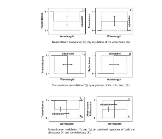
One way to improve the temperature control of optical coatings is to move from passive to active technologies. Instead of relying on the passive properties of materials to reflect a certain percentage of light, we can instead build thin film devices that are adjustable. By applying external stimuli, which can be pressure, light, heat, electrical potential or gas, some materials exhibit a change in their optical properties. These materials are defined as chromogenic for their ability to produce a visible or NIR transmittance change when the proper conditions are met. Upon removing the stimulus, or applying it in reverse in the case of a voltage, the device goes back to its original state. Integrating this type of material into the design of a window’s coating results in so-called “smart”
Figure 1.2: Transmittance modulation by regulation of absorbance (A), reflectance (R) and both. Adapted from [7].
windows, which can be used to modulate the transmittance at desired wavelengths through changes in absorbance, reflectance or both (see Figure 1.2).
One of the most studied materials for this type of application is tungsten trioxide (WO3) [6], [9], an electrochromic material which upon the application of an electrical potential changes from a transparent to dark blue state due to an increase in absorption in the red and near-infrared parts of the spectrum (see Figure 1.3. for an example of a window in different coloration states).
A controlled amount of light is allowed to pass through depending on how dark the device is, and the level of coloration is controlled by the intensity and length of the applied voltage pulse. This allows for a precise control over the solar heat gain of the window. Moreover, since the modulation also affects the visible part of the spectrum, one can envision the use of this same technology for privacy, light intensity control and user comfort. Compared to other types of chromogenic materials, WO3 also has the advantage of being user controllable and of being unaffected by light or temperature variations present in most real-life environments. It is also possible to power the device by simple means, requiring only a few volts of potential and minimal current to function, meaning that it can be implemented in most situations and might even be powered by another integrated device, such as a solar cell [10]. The device will then maintain its properties unless the reverse potential is applied, in a battery-like memory effect. More will be explained on the functionality of such devices in section 2.2.
The goal is to one day get to the point where a brick wall and a window façade posses similar thermal efficiencies. Presently, however, electrochromic devices have a few weaknesses over their passive counterparts: mainly high production costs and durability issues. On top of that, windows are, by design, meant to be installed and then forgotten but they are still held to incredibly high
standards and expected to last for decades. While this is feasible for more traditional low-e coatings, a smart window equipped with and advanced and dynamic nanotechnology-based thin film is much more susceptible to wear and tear. When held to such high standards, present EC devices are found lacking and a need for improved durability becomes apparent [9].
1.2 Context of the research
Climate change and the dangers that come with it is a subject that is very present on the mind of people around the world, who are more and more made aware of it. As there is an obvious link between fossil fuels, the world’s principal energy source, and the rapid deterioration of our ecosystems, it seemed to me that tackling the very wasteful ways we produce and use power was of considerable importance.
At the same time, through my years of studies at Polytechnique Montreal, I became aware of the world of thin films and their many uses through presentations of Prof. Martinu’s laboratory. Fascinated by their research, I was initially introduced to the field of EC materials through a summer internship focusing on interference-based optical security devices. A research project on the use of smart windows to improve energy efficiency seemed very interesting.
WO3 is the most promising material and one of major interest for Guardian Industries, one of the world’s top suppliers of architectural glass and a competitor of Saint-Gobain, Pilkington and Asahi Glass Co. With this industrial partner of the Multisectorial Industrial Research Chair in Coatings and Surface Engineering (MIC-CSE) chair interested in smart windows, we focused on improving some of its major flaws. Extensive research had previously been done by members of the laboratory on the best deposition conditions for the preparation of WO3 by sputtering [11]. In addition, previous work had shown that it was possible to improve the optical performance of WO3-based devices by transforming the single WO3 film into a dense and porous EC interference filter[12]. However, as the coloration mechanism of WO3 is triggered by the double insertion of electrons and ions [12], charge trapping was shown to a be problem in such multilayer architectures. We thus sought to develop a coating of WO3 with a much higher density which would impede the flow of protons while maintaining the required electron conductivity; this would allow us to isolate the electrochromic effect in the most appropriate layers.
One of the chosen avenues was to explore the use of substrate biasing, which results in ion bombardment of the sample’s surface during deposition and is known for increasing the density of the resulting film [13], [14]. As part of our methodology, we prepared films with substrate bias voltage going up to several hundred volts at low pressures as typical films are deposited at high pressures to ensure the generation of a porous microstructure. My initial results at low voltages showed the expected decrease in electrochromic activity. Only when increasing the bias voltage to much higher values did interesting effects occur.
In fact, after reaching a threshold potential, we started observing a behaviour which was opposite to the one expected for a denser layer. Instead of inhibiting the electrochromic effect, we suddenly obtained a layer that was not only highly efficient electrochromically but also much more durable than what had been observed during previous research [11], [15] (see figure 1.4).
Sensing how these results could potentially impact the field as well as intrigued by their counter intuitive behaviour, we shifted the focus of the project towards understanding what caused an improvement in performance of WO3 layers when very high energy ion bombardment was involved.
Figure 1.4 : Transmission variation (∆T) of preliminary samples of WO3 prepared with various applied substrate bias values.
1.3 Objectives
With the overall aim of improving the durability and performance of electrochromic WO3 thin films, the main objective of my project was defined as follows:
• Investigate the effect of high energy ion bombardment on the microstructure of WO3 thin films and their resulting electrochromic properties and durability.
To achieve this objective, a series of specific objectives were then defined:
1. Prepare WO3 thin films by magnetron sputtering while varying the applied substrate bias voltage.
2. Compare the resulting films’ electrochromic performance with the reference best-performing non-biased porous samples previously developed in the laboratory. 3. Analyse the composition, optical properties and microstructure of the produced
samples.
4. Establish a link between the effects of ion bombardment and the resulting structural changes in the WO3 thin films.
5. Evaluate which microstructure leads to the most efficient electrochromic behaviour coupled with the highest durability and why.
1.4 Scientific publications
Since common understanding of the use of substrate biasing would suggest a densification and deterioration of the EC performance of the films, the unexpected results we obtained formed the basis for an original research article that was submitted to the journal Applied Materials Today (see Table 1-1).
Table 1-1: Article accepted for publication in the context of my master's research project.
F. Blanchard, B. Baloukas, L. Martinu. Highly durable electrochromic tungsten oxide thin films prepared by high rate bias-enhanced sputter deposition, Applied Materials Today, 2018.
This research was also performed within the framework of the MIC-CSE chair and the results were judged as sufficiently of interest to apply for a patent to protect this discovery (see Table 1-2). Table 1-2 : Submitted patent related to the research project
No. PCT/US2017/050621 Title: Durable Electrochromic Device Including Tungsten Oxide Film Prepared In High Ion Bombardment And Low Pressure Deposition
Environment, And/Or Methods Of Making The Same
In addition to these publications concerning the main objective, additional work on integrating WO3 in thin film all-solid-state devices in the context of an INNOV grant on active security devices has lead to a presentation at the Society of Vacuum Coaters’ (SVC) 2017 technical conference, as well as an associated proceedings paper (see Table 1-3).
Table 1-3 : SVC proceeding paper
F. Blanchard, B. Baloukas, L. Martinu , All-Thin-Film Multi-Color Electrochromic Devices, 60th Annual Technical Conference Proceedings © 2017, Society of Vacuum Coaters Providence, Rhode Island, April 29-May 4, 2017
1.5 Thesis outline
Following the introduction, Chapter 2 of this thesis will present a literature review as well as the theoretical background required to understand the body of the work. Electrochromism plays a major role, with sections dedicated to its history, the functioning of an electrochromic device, the different materials that exhibit this behaviour, the effect of porosity on their performance, and the differences between amorphous and crystalline materials. A second part will focus on the fabrication methods of electrochromic thin films, such as e-beam evaporation and sol-gel, with a focus on sputtering. This will be mostly aimed towards how we can achieve a specific microstructure by controlling the deposition conditions.
Chapter 3 consists of the experimental methodology that was used throughout this project. To begin with, the bias-assisted RF magnetron sputtering process will be described, followed by the different
methods of optical characterization that were used. Afterwards, electrochemical and physical characterization methods will be presented.
Chapter 4 is dedicated to the article that was submitted for publication regarding the main objective of this research, which is presented as it was sent to the journal.
Chapter 5 will further discuss the results presented in the article and offer some additional perspectives. Nanostructured crystalline WO3, some other possibilities for high energy substrate biasing as well as a brief overview of my work on active security devices are the themes touched upon.
CHAPTER 2
LITERATURE REVIEW AND THEORETICAL
BACKGROUND
2.1 Foreword
This chapter presents the main theory and knowledge background in relation to the principal findings of this research. Electrochromism is a relatively well-known but not yet fully explored phenomenon that continues to attract the attention of a number of many researchers’ efforts around the world. Therefore, a significant amount of information may be found in the literature, either in journal articles or in books. While the most pertinent elements will be covered in this section, the reader interested in learning more on the subject is encouraged to consult the Handbook of Inorganic Electrochromic Materials by C.G. Granqvist [16] and Electrochromism and Electrochromic Devices by P.M.S. Monk, R. Mortimer and D. Rosseinsky [17] as excellent resources.
The present chapter focuses on thin film inorganic electrochromic materials. A brief history of electrochromic (EC) materials first introduces the context in this research takes place. An explanation of the phenomenon and how such films may be incorporated into functional devices follows.
WO3, as a model EC material, is then studied more in depth. Information on its atomic structure is given, as well as an explanation of the importance of controlling the microstructure of such films to achieve appropriate device performance. Finally, a comparison between the amorphous and crystalline phases of WO3 highlights their respective advantages and disadvantages.
Since the core of my project was directed towards modifying traditional deposition approaches by the addition of substrate biasing, a second section concerning the most popular fabrication methods of WO3 films follows. While e-beam and sol-gel preparation methods are briefly described, most of the information relates to sputtering and how a thin film’s microstructure and resulting properties can be controlled through a judicious control of the deposition conditions. Special emphasis is then put on the impact of ion bombardment as this clearly relates to our findings.
2.2 Electrochromism
The term electrochromism refers to, as the name suggests, coloration and electricity. More specifically, it describes the coloration phenomenon that some materials undergo when an electric potential is applied to them. As will soon be demonstrated, the coloration mechanism is related to an increase (reduction) or decrease (oxidation) in the number of electrons in the atomic system of such materials. Indeed, the displacement of these excess charges between energy levels following excitation is what causes the change in optical properties [16].
While there exist two main types of electrochromic materials, either organic or inorganic, only the latter ones are of interest in the present context due to several reasons. Indeed, although organic materials can exhibit faster coloration dynamics and more varied color changes, they suffer more from degradation than their inorganic counterparts [18]. Since device lifetime is of primary concern for smart windows, and considering this laboratory’s main expertise on inorganic thin films, the choice was clear. Of all the inorganic materials, the most famous of them is WO3, due to it being one of the first materials to be studied for this behaviour and its high coloration efficiency.
2.2.1 Historical background
The discovery of EC materials dates back to around 1704, when a painter named Diesbach discovered Prussian blue, a type of ferrocyanide that was largely used as a pigment in paints and inks [17]. Later on, the first demonstration of WO3 color changing properties was made by Berzelius in 1815, where the material heated in a hydrogen atmosphere switched from pale yellow to dark blue [19]. It was not until 1930 that the first electro-reduction of solid-state WO3 in an acid electrolyte, the same method that is used today to characterize the material, was realized by Kobosew and Nekrasson [17].
The first electrochromic device (ECD) is widely recognized as the prototype proposed by S.K. Deb in 1969 [17], [19]. Consisting of an amorphous WO3 thin layer evaporated on a quartz substrate, the color change was observed in plane upon applying an electrical potential between two regions. The particularity of this type of device was that there was no ion reservoir in contact with the layer, neither solid nor liquid. It was rather the ambient humidity that served as a hydrogen source, where moisture adsorbed on the surface of the device was dissociated upon the application of the electric current. This work by Deb then served as the basis for a multitude of applications involving
tungsten oxide. Early on, display systems were considered but none ever made it to commercialization mainly due to durability and switching speed issues. The first real commercial success was rear-view mirror with variable reflectance for the automotive industry [16], while present day efforts are mostly aimed towards smart windows.
2.2.2 Electrochromic materials
There exist three different types of electrochromic materials. There are materials that are soluble during their utilization, while others are soluble in their transparent form and solidify on the electrode after the coloring reaction. For practical reasons, when trying to build thin film-based devices both of these are not suitable. The third type of material which always remain solid is therefore favored – they include a range of transition metal oxides. Figure 2.1 displays which of these materials have a cathodic, anodic or dual behavior as in the special case of vanadium oxide [16].
While many different elements are capable of EC reactions, each has its own properties. The two most popular EC oxides are by far cathodic WO3 and anodic NiO, for the simple reason that they possess the highest coloration efficiency of their respective categories. WO3 is a cathodic EC material which is transparent in its natural state and displays a deep blue color upon ion intercalation. Nickel oxide is an anodic EC material which displays a yellow-brownish color in its colored state and becomes transparent upon ion intercalation.
Figure 2.1: Simplified periodic table of elements. Grayed transition metals are those with well documented cathodic and anodic electrochromism. Taken from[16].
Not much work was put into studying NiO during this master’s project as I focused my attention on WO3. However, NiO films were developed and tested in the context of all solid-state devices implemented for security applications as will shortly be discussed in Chapter 5.
2.2.3 Coloration mechanism
Let us now consider the mechanism behind the materials’ coloration. Upon the application of a voltage, electrons are inserted into the material and due to their negative charge, positively charged ions are then attracted maintain neutrality. It is this double charge insertion that leads to coloration in inorganic materials [20]. For cathodic EC materials, a simplified version of the reaction may be written as follows in the context of WO3:
WO3+ 𝑥 (𝑀++ 𝑒−) ↔ 𝑀𝑥WO3 (1) where M+ is a cation, x is the intercalation level and MxWO3 is the colored bronze state of WO3.
This process is called ion intercalation and usually involves small cations such as H+ or alkalines, such as Li+ and Na+ which diffuse into the material [21], [22]. A similar but reversed reaction is observed for anodic materials, which switch to a transparent state upon ion intercalation. For NiO, the hydrogen ion intercalation/deintercalation reaction can be summarized as follows:
𝑁𝑖(𝑂𝐻)2− 𝑥𝐻+ − 𝑥𝑒−↔ 𝑁𝑖𝑂
𝑥(𝑂𝐻)2−𝑥 (2) where NiOOH is strongly absorbing and the form Ni(OH)2 with an added cations is transparent [16].
From equation 1, we can already conclude that EC materials must be able to conduct electrons and allow for ionic diffusion. The physical reason why this charge insertion results in a color change, and why anodic and cathodic materials behave differently lies in their electronic configuration. Taking bleached WO3 as an example, when no charges are intercalated, the material is transparent in its semi-conductor state; this transparent state is typical of any semi-conductor with a large enough bandgap. For WO3, the bandgap lies in the UV at ~3.2 eV [23] while the Fermi level is under the conduction band between oxygen’s 2p and tungsten’s t2g orbitals [22] (see Figure 2.2
correspond to the dxy, dxz and dyz orbitals of a transition metal whose s and p electrons are fully ionized.
When ions and electrons are injected in a cathodic material, the t2g orbitals are the first to be filled
as they are more energetically favorable and the Fermi level rises into the t2g orbital. At this point,
WO3 becomes blue (HxWO3) either through an increase in absorption in the case of amorphous WO3 (a-WO3) or an increase in reflection for polycrystalline WO3 (c-WO3) both in the red and near-IR parts of the spectrum. Upon extraction, the Fermi level goes back down into oxygen’s 2p orbital and the material becomes once again transparent. For anodic materials, the Fermi level is already in the t2g orbital because of free electrons thus explaining their colored state. When
sufficient charges are inserted, the Fermi level rises above the t2g orbital and below the eg band;
providing the band gap is large enough and not in the visible, the material becomes transparent. Even though the coloration mechanism is still not entirely understood, the most accepted models make a distinction between the two phases. For crystalline WO3, the optical transition is caused by the electron band structure occupation change previously described, meaning that the electrons are free or quasi-free as in the Drude theoretical model. This model is also used to explain the behavior of metals, which are, in most cases, IR reflectors.
The amorphous material is instead described in terms of an intervalence charge transfer where the electrons are localized. Once a cation is intercalated, it is more favorable for it to form an OH group
Figure 2.2: Schematic band structure of different categories of EC oxides, cathodic (left) and anodic(right). Shaded regions denote filled states and E denotes energy. Taken from [16].
than a H2O molecule, until all oxygen atoms have been paired [24]. The W atoms will then switch between oxidation levels, with the charge transfer being powered by the absorption of incident photons, with the following reaction equation [25], [26]:
𝑊𝑖6++ 𝑊
𝑗5++ ℎ𝑣 ↔ 𝑊𝑖5++ 𝑊𝑗6+ (3) Reduction to a W4+ state is also possible but requires two electrons to reach the same site and is less probable. Transitions between these three states also mean different absorption mechanisms and the transition to that twice reduced state has also been identified as the main source of coloration in nanocrystalline WO3 synthesized via a sol–gel based dip coating process [25].
2.2.4 Electrochromic devices
Now that we know that double charge insertion is responsible for coloration, we must find a way to design a thin film stack that allows such a process to take place. Typical devices have two electrodes, an electrochromic layer, an electrolyte layer and an ion storage film. To be able to observe the color change, at least one of the electrodes needs to be transparent, which can be achieved with transparent conductive oxides (TCOs; e.g.: indium tin oxide (ITO), conductive nanowires, etc.). The substrate can be glass, in the case of a rigid device, or polymer sheets, for a
Figure 2.3: Generic five-layer electrochromic device design. Arrows indicate the movement of ions in an applied electric field. Taken from [16].
flexible version which allows roll-to-roll coating deposition. Figure 2.3 illustrates a popular configuration in the context of smart window applications.
When a negative potential is applied to the electrode in contact with the EC layer, electrons are injected into the EC layer and the cations leave the ion reservoir to complete the reaction described in Section 2.2.3. To be able to reach the active layer and counterbalance the charges, the ions must diffuse through an electrolyte layer that also serves as a barrier for electrons. This way, the charges are kept in the active layer even when the potential ceases to be applied and the device maintains its coloration (so-called memory effect). To revert to the device’s initial transparent state again, or in other words bleach it, the device may be short-circuited or the potential simply inverted, thus extracting the electrons and ions from the active layer, the latter returning to the ion storage layer. The electrolyte can be in liquid form, an acid for example may serve as a very efficient hydrogen source, in polymer form, which is extensively used in the context of flexible devices or in solid form. Polymer electrolytes decrease the probability of short-circuits because of their much larger thickness. Each form has advantages and disadvantages and must be chosen depending on the application. Electrochromic windows or glasses, for example, can pose the risk of breaking in proximity with people; using an acid as the electrolyte is then unacceptable. Some popular materials for electrolyte layers include SiO2, Ta2O5 and polycarbonate polymers containing a lithium salt, e.g. LiClO4 [16].
An interesting modification to this design is to implement an EC layer that is complementary to the active layer as a replacement of the ion reservoir, meaning that de device now has both anodic and cathodic EC materials. WO3 and NiO are most often the materials that are chosen for this configuration; NiO also being the most efficient inorganic anodic EC material. As both materials will now switch at the same time, WO3 turning blue during ion insertion and NiO turning brown upon ion extraction, the overall absorption will be higher and the resulting color will be more neutral than in the case of a single WO3 film. When inverting the potential, both materials will once again regain their transparency as the ions flow back from WO3 to NiO. Thus, by choosing the materials according to their tint it is possible to increase our control over the color of the whole device. Also, since hydrogen is often a critical component used to stabilize NiO into a favorable structure [16], it naturally lends itself to being a proton container for WO3. Note that the hydrogen
can be directly inserted during the deposition process, allowing for the entire deposition of a thin film device without the need to chemically add the cations before its completion.
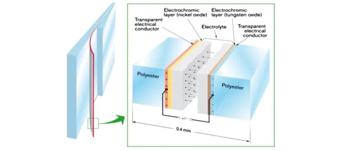
This type of device typically requires only a few volts to operate [16] and behaves as an open-circuit memory. Indeed, in the absence of current leaks, the desired level of coloration can be maintained without the use of additional power; in practice, current leaks are always present so that charge replenishing is required at specific intervals; still, minimizing these periods reduces the overall required power. An analogy between the EC device (ECD) and a battery is often made [26], [27] as the former also stores charges in addition to displaying an optical change. For real-life applications, these devices require a battery-like behavior to limit power consumption with the addition of minimal degradation over extended periods of time and following cycling. One example of present day smart window technology is applied to existing windows in the form of a foil, as shown in Figure 2.4 [26].
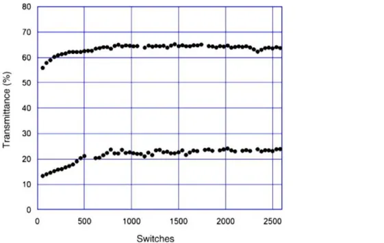
This particular configuration uses a thicker polymer-type electrolyte and can be expected to function for thousands of cycles with a stable transmission variation between the bleached and colored states (see Figure 2.5). Industry standards typically require a 10-20 years lifetime, corresponding to hundreds of thousands of cycles with minimum degradation. This represents a significant challenge which requires constant improvement in the properties of the participating
Figure 2.4: Principle of a construction of a foil-based EC device. The entire foil can be used to laminate glass panes, as shown in the left-hand part
.
Taken from [26].layers, particularly regarding the active EC WO3 layer for which durability issues are often reported [9], [12], [28].
2.2.5 Improving WO
3as an electrochromic material
Now that we know what EC materials are, how ion intercalation is responsible for their color change, and how a thin film device can allow such intercalation processes, we now focus our attention on the means to improve the device’s efficiency. To do so means finding ways to improve cations diffusion in and out of WO3 to achieve faster coloration speeds, whilst maintaining or improving the lifetime.
While many factors can influence cation displacement, ion diffusion is usually the one limiting the efficiency of an ECD [15]; one should note that electron diffusion coefficients are significantly higher, as fast as to 10-3 cm2/s in WO3 [15]. To improve the former characteristic, it is necessary to look at how the atomic structure impacts the insertion and extraction dynamics. Tungsten oxide’s crystalline structure is perovskite-like [29], which means it is composed of octahedral assemblies of a central tungsten atom surrounded by six oxygen atoms. These octahedra can either be joined
Figure 2.5: Transmittance for an EC foil device of the kind shown in Fig. 2.3 adjusted to a transmittance modulation ΔT of 55%. The panel shows evolution of the maximum and
by their corners or by their sides and the space in between them, called a B-site, can host small ions such as H+ or Li+ (see Figure 2.6) [23].
2.2.5.1 Porosity and performance
Naturally, for coloration to occur the cations must be able to reach these B-sites. A more efficient coloration process implies that it is easier for the ions to reach these sites and can be achieved by the addition of defects, which will disorganize the structure and facilitate ion insertion, and/or porosity in the material. For example, increasing a layer’s surface over volume ratio allows for more access points for the electrolyte to inject the ions into the WO3, especially when using a liquid electrolyte. For this reason, control over the microstructure of the prepared thin films is of the utmost importance for electrochromic materials.
A higher porosity typically leads to a film with deeper and faster coloration, but also lower mechanical and electrochemical durability. It is therefore necessary to reach a compromise between efficiency and durability, especially in the case of applications requiring thousands of activation cycles. This is even more important in the case of devices based on H+ insertion as such ions are known to potentially lead to damaging side reactions [15], [30]. In the context of sputtering, thin films of WO3 are usually prepared in their amorphous phase.
Apart from changing the growth process of the layer by varying the deposition pressure, there are other ways of inducing porosity in a thin film. One of these is to introduce defects in the microstructure, which can be achieved by inserting inclusions of an atom with a bigger lattice
parameter (Mo for example) in the material [17]. Perturbing the growth in such a way results in a more disorganized layer and in more space between the WO3 octahedra for ion diffusion. High energy ion bombardment can also cause similar defects by displacing atoms on the surface of the film as it grows. This method was extensively studied in the present project and will be discussed further in section 2.3.4.
2.2.5.2 Amorphous vs crystalline WO3
As previously mentioned, electrochromic WO3 is usually prepared in its amorphous phase. The main reason for this is a significant decrease in diffusion coefficient for the crystalline material. Indeed, a-WO3 grows as clusters of edge or corner sharing octahedra [16], meaning that there is a short-range order in the microstructure and that the layout is similar to the hexagonal crystalline phase (see Figure 2.7) [31]. This results in a material where the ions can easily move around the lattice and reach the insertion sites because of the large-scale disorder.
Conversely, WO3 prepared at high deposition temperatures or post-annealed will crystallize in a very ordered and much denser manner, leaving very little space for the ions to travel through. The diffusion coefficients for hydrogen ions are evaluated at ~10-8 cm2/s in a-WO3, compared to approximately 10-10 cm2/s in c-WO3 [17]. In practice, this means that a crystalline film will display little to no coloration compared to an amorphous film under the same conditions. This is even more of a problem when lithium ions are used for coloration, a very popular alternative due to reduced
degradation from side-reactions. Diffusion coefficients for Li+ are typically in the range of 10−11– 10−10 cm2/s for denser layers up to the range 10−9–10−8 cm2/s for more porous ones [24].
To be able to properly use crystalline WO3 as an electrochromic material, it is necessary to increase its porosity. An alternative is to produce a crystallized self-assembled mesoporous structure as was done by Sallard et al. (see Figure 2.8)[32], but this requires an additional sol-gel or other structuring procedure which is unrealistic for large-scale production using current industry standards.
The advantage of going through the effort of producing a porous c-WO3 is that a crystalline material is expected to be much more durable than an amorphous one and thus less subject to degradation over time. Another potential advantage in the case of smart window applications is that instead of becoming more absorbing as in the case of a-WO3, the intercalation process mostly increases the materials reflectivity in the red and near-IR regions, granting the film with low emissivity properties.
In summary, regardless of the coloration mechanism, ion intercalation is required to ensure the functionality of electrochromic materials. This means that thin films must be prepared keeping in mind that sufficient porosity is needed for adequate ion mobility and therefore for coloration to be Figure 2.8: Characterization of periodically ordered WO3 thin films after crystallization at 550 °C. Part a) shows a TEM image, which demonstrates the homogeneity of the mesopore structure. The inset presents an electron diffraction (ED) pattern recorded from the same localized area. Part b) shows two HRTEM images. Both ED and HRTEM confirm the high crystallinity of the pore walls. Part c) presents tapping mode AFM images, which show hexagonally arranged open pores at the surface. Taken from [32].
achieved. Although amorphous materials deposited at high pressure achieve this easily enough, to improve durability, a denser and/or crystalline material is favorable. To function, however, they require induced porosity in the microstructure, possibly by creating defects. This next section is therefore dedicated to understanding more about the thin film growth processes and how one can influence film properties by controlling the deposition conditions.
2.3 Fabrication methods
Thin film deposition technology covers a very broad range of applications, from highly resistant mechanical hard coatings to finely tuned optical filters. While niche applications may require specialty coatings using a specific deposition technology, most often, researchers have the choice of various deposition techniques to develop their coatings. That being said, each technique has its own advantages and disadvantages which need to be assessed in order for the resulting thin films to comply with the application requirements.
For a number of these techniques (mostly chemical and physical vapor deposition (CVD and PVD) processes), the system must be maintained under vacuum during deposition. Otherwise, at ambient pressure the mean free path would simply be too short for the particles to be able to reach the substrate. Vacuum is also critical to avoid any chemical side reactions between the deposited species and contaminants by limiting their presence. This is especially relevant for deposition of metals, where the presence of air (mostly nitrogen and oxygen) can lead to oxidation of aluminum or nitriding of titanium during their deposition, for example.
Sputtering was chosen as our preferred means of deposition as commercial viability was important; indeed, it is the preferred large scale industrial deposition technique for our industrial partner involved with this project, Guardian Industries. In the present context, controlling the microstructure of the film is what mainly interested us so the following section covers the well-known structure zone model as well as a literature review of the impact of ion bombardment on the growth of thin films. Nevertheless, a brief overview of other popular methods of WO3 thin film deposition is important to understand what they can offer in terms of structure control.
2.3.1 Electron-beam evaporation
As a physical vapor deposition technique, electron beam evaporation (a.k.a. e-beam evaporation) usually consists in a system where a crucible filled with the desired material is heated by an
accelerated electron beam, resulting in sublimation of the target material and subsequent precipitation of the vapor onto the substrate. By having more than one electron gun and target, co-deposition of two materials can be achieved.
One of the advantages of e-beam evaporation is that it takes place at very low pressures, meaning that no additional gases injection is required to preserve the stoichiometry of the material. This also results in a line-of-sight process, meaning that there is directionality to the growth of the film, which can be alleviated with rotation and translation of the sample holder if desired. This effect can be exploited to create interesting microstructures using the GLAD (glancing angle depositions) technique, which results in a columnar growth because of shadowing effects, with the amount of porosity depending on the relative angle between the incident material flux and substrate [12]. In addition, the voids can be filled with another material to create a composite layer.
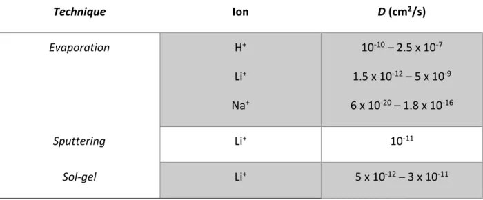
Evaporation systems and GLAD in particular have the advantage of potentially producing more porous materials than sputtering, resulting in greater values of ion diffusion coefficient; Table 2-1 gives values for evaporation, sputtering and sol-gel (data from [16]). The material is however very fragile and can be subjected to significant degradation after only tens of cycles in an aggressive environment, with H2SO4 as the electrolyte for example.
Table 2-1 : Diffusion constant of ionic species for WO3 thin films prepared by different techniques.
Technique Ion D (cm2/s) Evaporation H+ Li+ Na+ 10-10 – 2.5 x 10⁻⁷ 1.5 x 10⁻¹² – 5 x 10⁻⁹ 6 x 10-20 – 1.8 x 10⁻¹⁶ Sputtering Li+ 10-11 Sol-gel Li+ 5 x 10-12 – 3 x 10-11
Such systems can also be equipped with ion sources which allow for a controlled ion bombardment of the growing film’s surface. While of use for etching and cleaning, another advantage is ion-assist, which offers a greater control over the microstructure of the growing film. The effect is very similar to what happens when substrate biasing is introduced during sputtering, as will be discussed in Section 2.3.3.
Ion assist and GLAD can also be combined to achieve interesting properties by both increasing the amount of porosity with a high deposition angle and densifying the resulting columns with high energy bombardment, thus improving the durability of WO3 whilst maintaining performance. This approach is also under investigation in our research group and the subject of another master’s thesis.
2.3.2 Sol-gel
The sol-gel process is mostly used for producing metal-oxides from a colloidal solution (the sol) that transforms into an integrated network (the gel). The network can be constituted of discrete particles or polymer chains. This is a wet chemical process and therefore very different from vacuum-based PVD techniques, but still of interest to us because of the possibility to assemble crystalline nanoparticles of WO3 in an organized, porous network as mentioned in Section 2.2.5.2. A tungsten precursor is first dissolved in a proper solution, WCl6 in ethanol for example, then spin-coated and dried into an amorphous layer with a controlled microstructure. The material is then annealed at high temperature, crystallizing the tungsten oxide particles present in the network into a film that, if done correctly, will maintain its form [32], [33] (see Figure 2.8)
This evaporation-induced self-assembly can provide a three-dimensional mesoporosity, which is beneficial for cation insertion and thus the coloration process. The ion’s diffusion path length is shorter, and can consequently move more easily in the WO3 matrix. On top of that, the degree of crystallinity of the particles can be adjusted with the annealing procedure and the size of the nanoparticles controlled during the initial growth process [32].
While this method grants unprecedented control over the size, crystallinity and spacing of WO3 nanoparticles, allowing for the formation of a 3-D framework suited to an application’s needs, it was not investigated in the present project for several reasons. Firstly, the expertise of the FCSEL lies in the field of vacuum-based deposition technology, meaning that developing a completely
new sol-gel methodology would have been required. While this could have been surmounted, the same argument holds for our industrial partners who also prefer PVD-oriented processes. Finally, and perhaps the most compelling argument is that this method is much more complex, from the formation of the WO3 particles to the many subsequent sol-gel steps, especially from an industrial standpoint. Translating such a process to a large-scale production would present inherent limitations, a major drawback compared to the one-step solution we developed via ion-assisted sputtering.
2.3.3 Sputtering
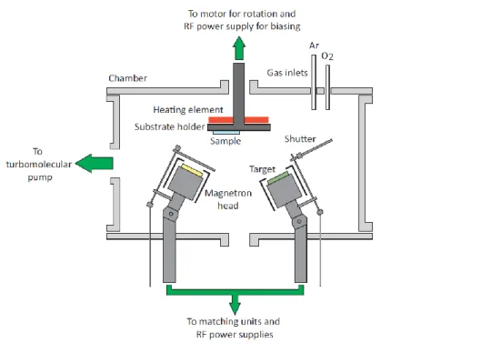
As was the case with e-beam evaporation, sputtering is a PVD technique but instead of vaporizing a sample with accelerated electrons, it relies on the momentum transfer from impacting ions. In its most simple form, DC (direct current) sputtering, a potential is applied between a target, the cathode, and the substrate holder which serves as the anode. Electrons present in the chamber are accelerated towards the anode and ionize a working gas inserted into the chamber, usually argon because it is the cheapest of the noble (inert) gases and easy to ionize. This generates a plasma, a neutral cloud of positively charged ions, electrons, neutrals and radicals. The positive ions are then accelerated towards the cathode and impact the target, transferring their energy. If the energy is high enough (another reason why argon, a relatively heavy noble gas, is used), meaning higher than the binding energy of the target material, atoms are ejected from it. The atoms then travel through the chamber and condense onto surfaces, including the sample held above (see Figure 2.9) [15].
Note that the schematic depicted in Figure 2.9 is for RF (radio-frequency) sputtering rather than DC. While they look similar, the difference resides in the type of power supply employed. The reason to use RF is that direct current sputtering may only be implemented with conductive targets; otherwise, it becomes impossible to sustain the discharge. RF sputtering was introduced to circumvent this problem: by applying a 13.56 MHz signal, the plasma frequency is increased, and a current can be applied on a dielectric target, with the additional advantage of an easier to sustain discharge thanks to higher discharge energy.
Since electrons have a much higher mobility than the ions, they can more easily follow the rapid change of polarity and the two electrodes appear negatively charged relative to the plasma. The equivalent circuit is two series of capacitors, one representing the target’s sheath and the other the substrate stage, connected to the chamber walls, baseplates, ground, etc. Since the capacitive reactance is inversely proportional to the area of the capacitor, the smaller sheath will see a much larger negative voltage. This ensures that most of the sputtering will occur at the target and not at the substrate [34].
Figure 2.9 Schematic representation of a chamber used for radio-frequency magnetron sputtering. Taken from [15].
Sputtering can also be done in a reactive environment, in which case gases such as O2, N2 and H2 are also introduced in the chamber. The reaction is then more complex, as target poisoning can occur, but allows for a greater control over the stoichiometry of the deposited film. It is also necessary if one wants to prepare an oxide from a metallic target, for example WO3 from W. In this project, both DC and RF methods were used and led to very similar results once the proper oxygen balance for sputtering from a pure W target was found.
The cathode in RF sputtering systems is also usually implemented as a magnetron, which consists of permanent magnets placed under the target. By superimposing a magnetic field to the electric field, a Lorentz force makes the electrons travel in a helical motion towards the target. This results in plasma confinement, increasing the ionization probability and therefore the plasma density. This correspondingly increases sputtering and, in turn, the deposition rate. Thanks to these higher rates, typically an order of magnitude higher than conventional sputtering, magnetron sputtering is the most widely employed commercial method [34].
2.3.3.1 Control of film properties through the control of deposition conditions
There are several parameters that can be adjusted in an RF sputtering system. The first one is the power applied between to the electrodes, which mainly controls the deposition rate by increasing the current density. A higher potential also means more acceleration for the ions in the plasma before they impact the target. This results in a greater momentum transfer, more atoms sputtered and a higher energy for these atoms. The growth of the film will be affected since more energy allows the atom to diffuse on the surface more easily, to reach a more ordered structure and usually producing denser films.
The power required varies between different materials and is dependent on the size of the target which is used, so it is more accurate to speak in terms of power density. One must also be careful not to damage the target by applying a potential that is too high. Because of thermal shock being a concern with dielectric targets, a ramping period is usually recommended. The way the power is applied also has importance. Pulsed-DC sputtering, for example, is used to minimize arcing and improve deposition rates for reactive sputtering of some dielectric materials like silica and alumina. Another method, high power impulse magnetron sputtering (HiPIMS), uses short bursts of very high-power density to achieve denser materials with improved adhesion.
![Figure 1.3: Coloration sequence of an electrochromic window [57].](https://thumb-eu.123doks.com/thumbv2/123doknet/2324785.30082/21.918.200.720.374.522/figure-coloration-sequence-electrochromic-window.webp)