UNIVERSITÉ DE MONTRÉAL
CONCEPTION ET RÉALISATION D’UN RÉCEPTEUR COMPOSÉ DE RÉSEAU D’ANTENNES YAGI MULTICOUCHES VERTICALES ET DE COMPOSANTS EN ONDES
MILLIMÉTRIQUES
OLIVIER KRAMER
DÉPARTEMENT DE GÉNIE ÉLECTRIQUE ÉCOLE POLYTECHNIQUE DE MONTRÉAL
MÉMOIRE PRÉSENTÉ EN VUE DE L'OBTENTION DU DIPLÔME DE MAÎTRISE ÈS SCIENCES APPLIQUÉES
(GÉNIE ÉLECTRIQUE) OCTOBRE 2010
UNIVERSITÉ DE MONTRÉAL
ÉCOLE POLYTECHNIQUE DE MONTRÉAL
Ce mémoire intitulé
CONCEPTION ET RÉALISATION D’UN RÉCEPTEUR COMPOSÉ DE RÉSEAU D’ANTENNES YAGI MULTICOUCHES VERTICALES ET DE COMPOSANTS EN ONDES
MILLIMÉTRIQUES
présenté par KRAMER Olivier
en vue de l’obtention du diplôme de Maîtrise ès Sciences Appliquées a été dûment accepté par le jury d’examen constitué de :
M. FRIGON Jean-François, Ph.D., président
M. WU Ke, Ph.D., membre et directeur de recherche M. TATU Serioja, Ph. D., membre
DÉDICACES
A ma compagne Danna, à ma famille et à mes amis.REMERCIEMENTS
Je souhaite remercier Pr. Ke Wu pour m’avoir accepté dans son équipe et guidé tout au long de ma maitrise ainsi que pour son aide financière.
Un grand merci aussi aux professeurs du laboratoire, notamment Mr. Cevdet Akyel pour son aide.
Je tiens aussi à remercier Mr. Jules Gautier, Mr. Steve Dubé, et Mr. Treian Antonescu pour leurs aides et conseils concernant la fabrication des circuits.
Je voudrais finalement remercier les personnes qui travaillent au laboratoire Poly-Grames, les étudiants, et plus précisément Mr. Tarek Djerafi et toutes les personnes avec qui j’ai partagé mon bureau.
RÉSUMÉ
Les applications en ondes millimétriques telles que les réseaux sans-fils haute vitesse demandent des composants de hautes performances, faibles coûts de revient, modulaires et compacts. Ce mémoire présente la conception d’une chaine de démodulation en ondes millimétriques utilisant le concept du multicouche.
Tout d’abord, une antenne Yagi multicouche est proposée et démontrée à 5.8 GHz. La structure utilise pour la première fois les éléments parasites des antennes Yagi dans une structure de substrats empilés verticalement. Cela permet d’atteindre un gain de 12 dBi. Deux configuration sont présentées : une première basée sur un dipôle et une deuxième basée sur un patch circulaire afin d’avoir une double polarisation. Les résultats mesurés montrent un très bon accord avec les simulations.
Basé sur les principes démontrés précédemment, l’antenne est adaptée à 60 GHz, puis un réseau d’antennes Yagi verticales en ondes millimétriques est introduit pour la première fois exploitant les technologies multicouches. Une analyse est faite pour définir les limites du design. L’antenne élément mesurée atteint un gain de 11 dBi. Le réseau 4x4 a une taille 50x50x60 mm3,
et atteint un gain mesuré de 18 dBi sur 7% de bande passante. Une autre configuration du réseau utilisant des antennes Yagi inclinées permet d’avoir une réduction des lobes secondaires tout en ayant un impact minimum sur le gain. Les antennes proposées sont d’excellents candidats pour des systèmes intégrés, faibles coûts, demandant une petite empreinte en ondes millimétriques.
Finalement, un nouveau six-port double couche utilisant des Guides Intégrés au Substrats (GIS) est présenté et démontré. Celui-ci permet de faire la démodulation QPSK. Son architecture utilise des coupleurs multicouches, fournissant une grande surface de couplage à travers deux fentes ; un déphaseur inédit, large bande composé de deux stubs plan-H et une ligne de référence ; ainsi que de deux diviseurs de puissance. Les simulations et mesures montrent que le circuit fonctionne correctement sur toute la bande V. La démodulation QPSK complète est testée sous le logiciel de simulation ADS et montre les excellentes performances du système.
ABSTRACT
Millimeter wave applications such as high-speed wireless connections require modular, compact-size, low-cost and high-performance systems. In order to realize a complete receiver satisfying those requirements, compact stacked multilayered designs are presented in this thesis.
First, high-gain compact stacked multilayered Yagi designs are proposed and demonstrated at 5.8 GHz. The structure makes use for the first time of vertically stacked Yagi-like parasitic director elements that allow easily obtaining a simulated gain of 12 dBi. Two different antenna configurations are presented, one based on dipole geometry for single polarization, and the other on a circular patch to achieve dual polarization. Measured results of the fabricated antenna prototypes are in good agreement with simulated results.
Second, based on the above-demonstrated principle, the antenna is redesigned and adapted for 60 GHz applications, and a novel design showing for the first time an array of Yagi elements in millimeter wave stacked structure is presented. An analysis is performed to define the structure limits. The measured element attains 11 dBi of gain. The proposed 4x4 array has a size of 50x50x60 mm3, and reaches a measured gain of 18 dBi over 7% of bandwidth. An alternative
configuration of the array using angled Yagi antenna elements allows for a significant improvement of the side lobe level without a visible impact on the gain. The proposed antennas present excellent candidates for integrated low-cost millimeter-wave systems that require small footprint.
Third, a novel dual layered six-port front-end circuit using the Substrate Integrated Waveguide (SIW) technology is presented and demonstrated. The six-port architecture makes use of multilayer couplers, providing a wide coupling area through two slots; a new broadband SIW phase shifter composed of two H-plane stub lines and one reference line; and two SIW power dividers. Simulation and measurement results show that the proposed six-port circuit can easily operate at 60 GHz for V-band system applications. The complete QPSK demodulation is tested through the ADS simulation platform to prove the good performances of the designed circuits.
TABLE DES MATIÈRES
DÉDICACES ... III REMERCIEMENTS ... IV RÉSUMÉ ... V ABSTRACT ... VI TABLE DES MATIÈRES ... VII LISTE DES FIGURES ... IX LISTE DES SIGLES ET ABRÉVIATIONS ... X LISTE DES SYMBOLES ET ABRÉVIATIONS ... XI
INTRODUCTION ... 1
DÉMARCHE GÉNÉRALE ... 6
CHAPITRE 1 ANTENNES À 5.8 GHZ ... 7
1.1 Théorie des antennes Yagi-Uda ... 7
1.2 Présentation de la réalisation ... 9
1.3 Article 1 - Vertically Multilayer-Stacked Yagi Antenna with Single and Dual Polarizations ... 10
1.3.1 Introduction ... 11
1.3.2 Antenna design consideration ... 15
1.3.3 Results and Discussion ... 24
1.3.4 Conclusion ... 29
Acknowledgment ... 30
References ... 30
CHAPITRE 2 ANTENNES À 60 GHZ ... 33
2.1 Présentation ... 33
2.2 Article 2 - Very Small Footprint 60 GHz Stacked Yagi Antenna Array ... 34
2.2.1 Introduction ... 35
2.2.2 Stacked Yagi Antenna ... 37
2.2.3 4x4 stacked Yagi Antenna Array using SIW feeding Mechanism... 41
2.2.4 Low Side Lobe Level (SLL) 4x4 Array of stacked Yagi Antenna with slanted elements ... 48
2.2.5 Conclusion ... 49
Acknowledgment ... 50
References ... 50
CHAPITRE 3 DÉMODULATION ... 53
3.1 Choix du circuit de démodulation ... 53
3.2 Présentation du six-port ... 53
3.3 Théorie du six-port ... 54
3.3.1 Origine ... 54
3.3.2 Réflectométrie ... 54
3.4 Jonction six-port modifiée ... 59
3.4.1 Présentation ... 59
3.4.2 Démodulateur ... 61
3.4.3 Fonctionnement en tant que discriminateur de phase ... 62
3.5 Présentation de la réalisation d'une jonction six-port modifiée à 60 GHz ... 65
3.6 Article 3 - Dual-Layered Substrate Integrated Waveguide Six-Port with Wideband Double Stub Phase Shifter... 66
3.6.1 Introduction ... 67
3.6.2 Design Framework ... 69
3.6.3 Simulated and Measured Results ... 74
3.6.4 Conclusion ... 78
Acknowledgment ... 81
References ... 81
CHAPITRE 4 CIRCUIT EN BANDE DE BASE - DÉCODEUR I/Q ... 83
4.1 Présentation ... 83
4.2 Simulations et mesures de la jonction six-port ... 83
4.2.1 Configuration ... 83
4.2.2 Résultats ... 85
CHAPITRE 5 DISCUSSION GÉNÉRALE ... 89
CONCLUSION ET TRAVAUX FUTURS ... 90
LISTE DES FIGURES
Figure 0.1 : Représentation de la chaine de réception. ... 2
Figure 0.2 : Représentation d’un système intégré multicouche. ... 2
Figure 1.1. : Schéma de base du concept d’antenne Yagi-Uda. ... 7
Figure 1.2 : Schéma montrant le rôle du directeur dans les antennes Yagi. ... 8
Figure 1.3 : Gain (dB) versus Nombre d’Éléments (N). [Stutzman et Thiele (1998)] ... 9
Figure 3.1 : Schéma d'un réflectomètre six-port. ... 55
Figure 3.2 : Schéma d'un six-port. ... 56
Figure 3.3 : Solution graphique aux équations du six-port afin de trouver Γ. ... 58
Figure 3.4 : Schéma montrant différents placements des points q. ... 59
Figure 3.5 : Schémas des composants du six-port modifié. ... 60
Figure 3.6 : Jonction six-port modifiée classique. ... 61
Figure 3.7 : Démodulateur utilisant une jonction six-port. ... 62
Figure 3.8 : Position des points pour θ5=π/4. ... 64
Figure 3.9 : Modulation QPSK. ... 65
Figure 4.1 : Diode Schottky. ... 83
Figure 4.2 : Modélisation du détecteur de puissance. ... 84
Figure 4.3 : Circuit soustracteur à l’aide d’amplificateurs. ... 84
Figure 4.4 : Schéma de la simulation ADS de la conversion directe. ... 85
Figure 4.5 : Signaux d’entrée et sortie. ... 86
Figure 4.6 : Spectre du signal modulé QPSK d’entrée. ... 87 Figure 4.7 : Courbes simulées et théoriques du taux d’erreur de bit pour une modulation QPSK.88
LISTE DES SIGLES ET ABRÉVIATIONS
ADS Advanced System Design
AGC Automatic Gain Control
BER Bit Error Rate (taux d’erreur global)
DUT Device Under Test
FPB Filtre passe bas
GIS Guide Intégré au Substrat (Cf. SIW) HFSS High Frequency Structure Simulator
IEEE Institute of Electrical and Electronics Engineers
LNA Low-Noise Amplifier
LO Local Oscillator (Oscillateur Local) LTCC Low Temperature Co-fired Ceramic QPSK Quadrature Phase Shift Key
RF Radio Fréquence
S/N Signal to Noise Ratio
SIW Substrate Integrated Waveguide (Cf. GIS)
SLL Side Lobe Level
LISTE DES SYMBOLES ET ABRÉVIATIONS
λo Longueur d'onde en espace libre
µ Perméabilité magnétique
c Vitesse de la lumière dans le vide
F Fréquence Z0 Impédance Caractéristique Γ Coefficient de réflexion ε Permittivité électrique εr Permittivité relative λ Longueur d’onde ω Fréquence angulaire
INTRODUCTION
Les ondes millimétriques correspondent aux fréquences dont la longueur d’onde est de l’ordre du millimètre, i.e. les fréquences de 30 à 300 GHz. Elles ont l’avantage d’offrir des plus grandes largeurs de bande disponibles, des circuits plus petits ou des antennes avec un meilleur gain. Comme exemples d’application, on peut citer les systèmes de positionnements locaux, les systèmes de télécommunication ou encore l’imagerie (médicale ou de sécurité). Les circuits les composant doivent être simples, à la fois robustes et fiables, ayant des coûts de fabrication faibles et une consommation réduite.
Entre autre, l’utilisation de la plage de fréquences allant de 57 à 67 GHz dans la bande V gagne rapidement de l’intérêt, car cette bande libérée en 2001 donne la possibilité à des transferts de données hauts débits. Les réseaux sans-fils intérieurs de plusieurs Gb/s ou la transmission de films haute définition non-compressés, figurent parmi les applications. La majorité des pays a libéré cette bande et possède 5 GHz de spectre continu en commun, évitant ainsi les problèmes de régulation entre pays. La communauté scientifique a répondu à cette récente attention en proposant des circuits à ces fréquences [Bosco et al. (2004), Sum et al. (2009)] et en mobilisant leurs efforts vers une standardisation internationale. Parmi celles-ci, on peut citer IEEE 802.15 Task Group 3c (TG3c) [IEEE 802.15] ou IEEE 802.11 Task Group ad (TGad) [IEEE 802.11].
Les circuits en ondes millimétriques doivent répondre aux besoins demandés par ces applications devenant de plus en plus exigeantes. Plus spécialement, la tendance aujourd’hui est de pouvoir combiner intégration et performance [Sun et al. (2006), Gunnarsson et al. (2005)].
L’étude faite dans ce projet de maitrise consiste en la réalisation des composants essentiels d’une chaine de réception (front-end) fonctionnant dans la bande V. L’utilisation de structures multicouches est privilégiée afin de démontrer la haute intégrabilité et les avantages en termes de performance qui peuvent être atteints. L’intégration multicouche de composants coupe avec les technologies actuelles majoritairement planaires et dont l’apport d’une nouvelle dimension ouvre de nouvelles possibilités. L'utilisation des GIS (Guides Intégrés au Substrats ou Substrate Integrate Waveguide en anglais) est privilégiée. Ce guide construit directement à partir d'un substrat planaire, confine le champ électromagnétique à l’aide de deux rangées de trous métalliques. Cette technologie permet de ne pas avoir des pertes par radiation et en conséquence de ne pas perturber les éléments proches.
Ce travail traite de la conception des trois grandes parties dont est composé la chaine de réception à conversion directe basée sur un six-port (Cf. Figure 0.1) : l’antenne de réception, le démodulateur, et le circuit en bande de base de décodage. Le but est d’intégrer ces éléments au sein d’une même technologie pour obtenir un système compact (Cf. Figure 0.2).
Figure 0.1 : Représentation de la chaine de réception.
Figure 0.2 : Représentation d’un système intégré multicouche.
Le premier chapitre du projet propose la réalisation d’une antenne à haut gain. Pour cela une structure unique, se basant sur le principe de conception d’antennes directives découvert par Hidetsugu Yagi et Shintaro Uda, est étudiée.
Cette antenne reprend les règles de conception introduites par Yagi-Uda mais dans une structure faite de substrats empilés afin d’avoir une antenne multicouche, performante, et donnant de nombreuses possibilités d’alimentation (dual-polarisation, etc.). La superposition verticale de substrats à permittivité élevée permet d’avoir un nombre de directeur élevé tout en restant
Antenne Démodulateur Récupération de l’information Circuit en bande de base Chaine de réception 0 1 0 0 1 1 1 0 1 1 0 0 01 0 Diodes RF Ampli. FPB Antenne LNA Démodulateur Six-Port LO
compact, et donc avoir un gain important comparé aux antennes Yagi microstrip planaires à même nombre d’éléments. Afin de faciliter la phase de conception, deux premiers designs sont étudiés à 5.8 GHz vérifiant le fonctionnement du principe introduit, mais sans les contraintes de fabrication, de mesures (analyseur réseau et chambre anéchoïque) présentes à 60 GHz. Ces deux designs ont été réalisés : un premier basé sur un dipôle imprimé sur substrat ; un deuxième basé sur une antenne patch circulaire permettant des polarisations orthogonales. Une étude approfondie des paramètres critiques à la conception a été faite, comme sur la taille du plan de masse (réflecteur).
Le deuxième chapitre se base sur les bons résultats obtenus précédemment pour concevoir une structure fonctionnant à 60 GHz. Étant donné que l’espacement entre les éléments de l’antenne Yagi est inversement proportionnel à la fréquence, cette structure devient très attractive à hautes fréquences car elle devient exceptionnellement compacte et les espaces d’air requis entre les couches à basses fréquences (comme à 5.8 GHz) disparaissent. Cet élément fonctionnant à 60 GHz est ensuite repris pour être adapté en un réseau 4x4 d’antennes Yagi réalisé en utilisant la technologie des GIS. L’antenne créée atteint un gain de 19 dBi avec une empreinte minimale (un réseau planaire classique de même gain est quatre fois plus étendu en surface). En ajoutant plus d’éléments, un gain très élevé peut être réalisé tout en ayant une bonne efficacité, ce qui en fait un candidat parfait pour les systèmes d’imagerie. Le réseau possède de plus la possibilité d’orienter chaque élément qui le compose. Cela permet de pouvoir manipuler la forme du faisceau d’antenne (en réduisant par exemple les lobes secondaires, avoir une meilleure largeur de faisceau, etc.) ou de pouvoir augmenter la bande passante. Une antenne utilisant ce dernier principe et minimisant le niveau des lobes secondaires a été conçue et mesurée.
Le troisième chapitre consiste en un système de démodulation compact, performant et multicouche. Par rapport aux récepteurs hétérodynes conventionnels, les récepteurs à conversion directe permettent la réduction de la complexité du circuit, un niveau élevé d’intégration et une réduction du taux d’erreur de bit en diminuant les imperfections de fabrication. Pour ces raisons, un démodulateur six-port passif utilisant la technologie des GIS a été choisi. Cette plateforme développée pour la première fois permet de tirer avantage de la large surface de couplage planaire des coupleurs et utilise un déphaseur inédit, large bande, basé sur des stubs plan-H. Ce déphaseur a été modélisé mathématiquement, simulé et réalisé. Le six-port complet réalisé montre d’excellentes performances en phase et en amplitude sur toute la bande allant de 55 à 65 GHz.
Le quatrième chapitre étudie le circuit en bande de base du démodulateur permettant la récupération de l’information. Les performances du système de démodulation couplé avec le six-port sont étudiées.
Finalement, ce travail est conclu en mettant en avant les nouveaux concepts présentés et leurs possibles évolutions.
Ce mémoire montre les résultats qui peuvent être atteints en technologie multicouche et analyse les phénomènes mis en jeux. Ces résultats peuvent facilement être réalisés avec les nouveaux processus comme le LTCC ou la technologie film-épais photosensible permettant ainsi d’atteindre des fréquences plus élevées et d’automatiser la conception. Les principales contributions originales apportées par ce mémoire sont :
• Une nouvelle topologie d'antenne Yagi à substrats empilés a été proposée. Le fonctionnement et les propriétés de ces antennes ont été montrés à 5.8 GHz (pour des applications de plateformes de positionnement local, de systèmes de capteurs sans fils et de radars) et en fréquences millimétriques. Elles permettent la création d’antennes passives à haut gain ayant une grande flexibilité d’alimentation (e.g. dual-polarisation). Une méthode de conception systématique et les limitations de cette structure sont présentées.
• L’antenne Yagi élément a été adaptée avec succès dans un réseau d’antenne fonctionnant à 60 GHz. Cette structure est attrayante car elle apporte les avantages des réseaux à celle-ci. Ces antennes ont la possibilité d’atteindre un gain très élevé. Elles sont peu couteuses, ont une empreinte plus petite que les antennes actives utilisées actuellement en hautes fréquences et les systèmes basés sur celles-ci consomment moins. Cela en fait une plateforme idéale pour les domaines de l’imagerie millimétrique ou térahertz (de sécurité, médicale ou pour l’aéronautique).
• L’utilisation de différentes orientations d’antennes au sein du réseau (utilisant les propriétés des antennes Yagi) a permis de modifier le diagramme de rayonnement pour réduire le niveau des lobes secondaires. Cette caractéristique peut permettre de résoudre les problèmes de trajets multiples (en plaçant des zéros sur le diagramme de rayonnement), d’augmenter l’angle de balayage électrique d’un réseau ou d’adapter le rayonnement de l’antenne à chaque application.
• Un six-port double couche a été conçu, fabriqué et mesuré. Sa topologie est étudiée afin qu’il possède six accès exactement contrairement aux configurations classiques à huit accès
(nécessitant leur adaptation). Son comportement, son fonctionnement et son efficacité ont été simulés dans le système global.
• Une étude exhaustive du nouveau déphaseur contenu dans le six-port a été faite, avec un modèle prédisant les résultats de simulations et de mesures.
• L’intégration en GIS du réseau d’antenne et du six-port permet d'obtenir une excellente isolation entre les éléments du canal réception, évitant les problèmes d’interférences.
Ce mémoire est présenté par article et reprend trois articles dont je suis l’auteur et le contributeur principal: un publié dans IEEE Transaction on Antennas & Propagation et deux soumis respectivement dans IEEE Transaction on Antennas & Propagation et IEEE MTT-S Transaction. Il est aussi à noter que les antennes présentées ici ont été reprises par des doctorants afin de les adapter à plus hautes fréquences et qu’un processus de valorisation est entrepris avec l’École Polytechnique de Montréal et Univalor afin d’explorer leur potentiel.
DÉMARCHE GÉNÉRALE
Ce mémoire présente trois articles intégrés dans le corps du travail. Le premier article intitulé “Vertically Multilayer-Stacked Yagi Antenna with Single and Dual Polarizations” a été publié dans IEEE Transaction on Antennas & Propagation en avril 2010. L’article intitulé “Very Small Footprint 60 GHz Stacked Yagi Antenna Array” a été soumis dans IEEE Transaction on Antennas & Propagation le 25 novembre 2010 et l’article “Dual-Layered Substrate Integrated Waveguide Six-Port with Wideband Double Stub Phase Shifter” dans IEEE MTT-S Transaction le 25 novembre 2010. Ces revues ont été choisies car elles sont reconnues mondialement et font office de référence dans le domaine des antennes et des circuits passifs micro-ondes. La rédaction des articles a fait l’objet d’un soin poussé afin de répondre aux contraintes de rigueur et d’analyse demandées par les revues prestigieuses et par ce mémoire de maitrise. La rédaction des articles est condensée afin de respecter les normes d’espace et de mise en page, imposées par les publications. Chaque chapitre se concentre sur une étape de conception du système. Avant chaque article, une présentation est faite afin de donner le contexte de l’article, les informations théoriques nécessaires à sa compréhension ainsi que la littérature pertinente. Les articles sont insérés au fil de la démarche de travail permettant d’aider à la compréhension.
Les trois articles ont comme auteurs : moi-même, Tarek Djerafi et Ke Wu. Les simulations, le développement, l’envoi en fabrication, les mesures, les expérimentations et la rédaction des articles a été faite par moi. Tarek Djerafi et Ke Wu m’ont conseillé et m’ont apporté leur expérience tout au long des travaux. Ils m’ont aussi aidé concernant les standards de rédaction d’articles IEEE. Le pourcentage de ma contribution réelle par rapport à celles des autres coauteurs est d’environ 75%.
CHAPITRE 1 ANTENNES À 5.8 GHZ
1.1 Théorie des antennes Yagi-Uda
Ayant besoin d’une antenne avec un gain relativement élevé, l’antenne de type Yagi-Uda se révèle être un excellent candidat pour l’antenne de réception de notre système [Yagi (1928), Uda (1930)]. L’antenne de Yagi est devenue très populaire en raison de sa simplicité et de son gain élevé réglable (une antenne Yagi de trois éléments peut atteindre un gain de 9dB une fois optimisée). Une antenne de Yagi-Uda de trois éléments se compose d'un dipôle (aussi appelé conducteur/driver) de longueur λ/2, soutenu par un réflecteur légèrement plus long et un directeur de l'autre côté (Cf. Figure 1.1.). L’application générale la plus connue de l’antenne Yagi-Uda est l’antenne de télévision UHF.
Figure 1.1. : Schéma de base du concept d’antenne Yagi-Uda.
Dans ce type d’antenne, seul le dipôle est alimenté. L’élément réflecteur, comme son nom l’indique, réfléchit les champs afin d’augmenter le gain dans la direction voulue.
Les directeurs auront un courant induit par l’émission du dipôle et émettront à leurs tours. Leur position doit être soigneusement choisie pour que l’ensemble des champs rayonnés par les éléments de l’antenne, s’additionne dans la direction voulue et s’annule dans la direction opposée. La Figure 1.2 [Wikipedia.fr] représente ce qui se passe avec une antenne constituée d’un dipôle et d’un directeur, ainsi que l’amplitude du champ. Le directeur est placé à une distance de λ/10 (36° de déphasage) du dipôle. Le retard de phase de courant du directeur peut être ajusté en modifiant sa longueur. Cette longueur est définie pour que l’onde arrière soit en
opposition de phase avec celle du dipôle rayonnant, i.e. une phase de 180-36°=144°. La représentation montre l’onde arrière réduite ainsi que l’addition des champs sur l’onde avant.
Figure 1.2 : Schéma montrant le rôle du directeur dans les antennes Yagi.
L’espacement horizontal entre les directeurs d’une antenne Yagi de plus de trois éléments est proche de : d≈λ/4 dans l’air (λ étant la longueur d’onde de l’antenne), mais peut varier entre 0.1λ et0.3λ. Une antenne Yagi peut atteindre un gain assez élevé mais est toutefois limité, et sature au delà de dix directeurs à environ 12.5 dB (Cf. Figure 1.3).
Dipôle Onde avant Onde arrière So m m e A m plitu de Emission du dipôle Emission du directeur Directeur
Figure 1.3 : Gain (dB) versus Nombre d’Éléments (N). [Stutzman et Thiele (1998)]
1.2 Présentation de la réalisation
L’idée générale est de pouvoir fabriquer une antenne Yagi-Uda multicouche (plusieurs couches empilées) afin de garder les performances et avantages d’une telle structure tout en ayant une configuration compacte et intégrable. Dans la cadre de ce travail, une première étude a été faite sur ce type d’antenne à 5.8 GHz. Cela a permis de définir les règles de design, les caractéristiques d’une telle antenne, les paramètres critiques et d’étudier la structure à une fréquence de travail plus aisée qu’en ondes millimétriques.
1.3 Article 1 - Vertically Multilayer-Stacked Yagi Antenna with
Single and Dual Polarizations
Olivier KRAMER, Tarek DJERAFI, and Ke WU, Fellow, IEEE
“Vertically Multilayer-Stacked Yagi Antenna with Single and Dual Polarizations”
Publié dans “IEEE Transactions on Antennas and Propagation” en Avril 2010, dans le Volume: 58 Issue:4, pages: 1022 - 1030
Abstract— There are many applications such as local positioning systems (LPS) and wireless sensor networks that require high-directivity and compact-size antennas. The classical Yagi-Uda antenna may be useful in meeting such demands, which however, becomes very large in size to achieve a high-gain performance due to a large number of directors as well as space required between those elements. In this paper, high-gain yet compact stacked multilayered Yagi antennas are proposed and demonstrated at 5.8 GHz for LPS applications. This structure makes use of vertically stacked Yagi-like parasitic director elements that allow easily obtaining a simulated gain of 12 dB. Two different antenna configurations are presented, one based on dipole geometry for single polarization, and the other on a circular patch to achieve dual polarization. The characteristics of these antennas with respect to various geometrical parameters are studied in order to obtain the desired performance. Measured results of the fabricated antenna prototypes are in good agreement with simulated results. The measured dipole Yagi antenna attains 11 dB gain over 14% bandwidth with a size of 80x80x29mm3. Radiation patterns of the dual-polarized Yagi antenna are nearly identical to those of the single-polarized antenna, which has a size of 50x50x60mm3, and also its two-port isolation is found to be as low as -25 dB over 4% bandwidth. The proposed antennas present an excellent candidate for compact and low-cost microwave and millimeter-wave integrated systems that require fixed or variable polarization capabilities and small surface footprint.
Index Terms—Microstrip antenna, Yagi-Uda, stacked antenna, dipole, circular patch, balun, dual polarization.
1.3.1 Introduction
he Local Positioning System (LPS) is a radio system used to search for and track down in real time objects of interest within a limited space range. This is a typical application of wireless sensor networks. With the LPS, a mobile object can be localized and can also collect information about its position at a precise time instant [1]. Applications of such a LPS system are multiple and diverse. Those systems are used for zone security with great efficiency, particularly indoor applications such as at airports where security is mandatory. Also location tracking can
clearly improve maneuver of the business and logistics management, for example, hospitals can improve their healthcare services by keeping a constant track of the location of doctors, nurses, etc. LPS can also be used in many other applications such as construction and agriculture, leisure and sports, etc. For a full integration with GPS systems that are usually used for outdoor scenarios, LPS is expected to achieve the challenging task of being accurate, low-cost and autonomous at ISM frequencies such as 5.8 GHz. Therefore, compact, light and low-cost antenna is required for such LPS design and implementation.
The Yagi antenna, which has been very popular because of its simplicity as well as its customizable high gain (three-element Yagi antenna can reach 9 dB when optimized) [2], can be used for this type of applications. The basic unit of a three-element Yagi antenna consists of a half-wavelength driver dipole backed by a longer reflector and a director on the other side.
Several microstrip-based Yagi or quasi-Yagi antenna structures have been reported in the literature [2]-[8]. Interesting approaches are related to the design of a microstrip Yagi array based on the microstrip patch antenna such as the array developed in [3] for mobile satellite system in the L-band. The antenna developed was based on patches, consisting of one reflector, one driving element and two directors. An array of four antenna elements was successfully used to achieve the required performance. The design reported in [4] was made on the basis of patches instead of dipoles as the driver element. An interesting printed Yagi antenna configuration was presented in [5], [6] where the Yagi-like printed dipole array antenna was fed by a microstrip-to-coplanar strip transition. In this case, a truncated microstrip ground plane was utilized as a reflecting element. On the other hand, an active quasi-Yagi version was proposed [7] for 5.8 and 60 GHz applications. In [8], the proposed antenna consisted of a dipole as a driving element, a parasitically coupled reflector and six directors. The antenna was designed by utilizing the same design rules as used in the conventional Yagi dipole antenna while taking into account the fact that the antenna was made on a planar substrate. The antenna was designed for 5 GHz band and has achieved a gain of 10dB.
To overcome the problem of size and footprint within the planar structure, two novel high-gain compact structures based on the Yagi-Uda antenna concept are presented for the first time in this work. These structures are constructed in a multilayer topology by stacking together the reflector, the driver, and the directors. Compared to the above-described uniplanar Yagi antennas, this design is able to provide a number of advantages. First of all, the usage of the third dimension
(the vertical dimension) that has not been widely used in the design of microstrip antennas, allows an effective reduction in size and footprint. In fact, multilayer processing techniques have become more mature in integrated circuit design, fabrication and integration. Second, a high permittivity substrate can be used in this case, thereby reducing spacing between the directors, which is critical for a high-density integration between antenna and circuits. Third, the possibility of a dual polarization design based on the Yagi antenna concept is made possible, and the coupling-based feed mechanism can achieve wide bandwidth characteristics.
Various stacked structures were investigated as in [9] and [10]. The advantage of those topologies is that substrate thickness can be adjusted to achieve an optimized bandwidth performance. Unlike the Yagi antenna, which is a traveling-wave antenna [11], the structure is a resonant mode antenna. In the Yagi structure, the director is smaller than the driver and the distance between them is between 0.2λ and 0.45λ. In [9] the thickness of the used substrate is about 0.015λ, the bandwidth is 70 % wider than the single patch without gain improvement and the upper layer patch is bigger. Li studied theoretically different patch shapes (square, circular, triangle, etc.) and investigated the optimal combination to achieve a lower cross polarization or circular polarization [10]. The substrate to wavelength in the dielectric ratio is close to 0.02. Stacked triangular microstrip antennas were also investigated experimentally in [12] to achieve a bandwidth about 17-5% at the centre frequency of 3.407 GHz.
To demonstrate the proposed concepts and design features, we will present two case studies in connection with the design of respective structure. The first design (see Fig. 1) is a multilayered printed-circuit version of the proposed Yagi antenna. It consists of a ground plane (as a reflector), a dipole (as a driver), and four directors. In the second design (see Fig. 3), the antenna presents a dual polarization using circular patches in the design of one driver element and four directors.
Fig. 1. Proposed structure of design 1 (dipole stacked Yagi antenna).
Fig. 3. Proposed structure of design 2 (dual polarization circular patches).
In this paper, the configuration of the proposed Yagi-Uda antenna is described in detail. Design specifications are discussed, considering the effects of different dimensions on antenna performances. Both proposed antennas as described in Fig. 1 and Fig. 3 are fabricated. Simulated and measured results are then compared, and the work is finally concluded.
1.3.2 Antenna design consideration
1.3.2.1 Dipole Stacked Yagi Antenna (Design #1)
The configuration of the dipole stacked Yagi antenna shown in Fig. 1, is based on the classical Yagi-antenna design principle. It consists of one dipole driver element, and four parasitic elements. The antenna is designed on the basis of the same design rules that are used in the conventional Yagi dipole antenna, except that the antenna is made on a planar substrate.
There have been many different design versions for printed dipole antennas and baluns, as well as coplanar strip dipoles fed by coplanar waveguide and stripline balun used to feed a printed quasi-Yagi antenna proposed in [5]. The proposed dipole allows the avoidance of a balun which becomes usually necessary when dipole antennas are fed by an unbalanced line. The dipole (layer II in Fig. 1) is printed on both sides of a dielectric substrate [13], [14], [15]. The bottom-tapered
ground transition is designed to provide an impedance matching tuner with balanced output. The designed feed network of the dipole antenna with the tapered balun transition is tuned by the angle of the tapered ground plane for impedance matching and balanced output. This simplified feeding structure results in the reduction of transmission line length and in turn radiation loss. Moreover, it has attractive wide bandwidth capabilities. The feeding dipole bandwidth (without any Yagi antenna elements) is relatively large; a bandwidth of 29% can be achieved at 5.8GHz using a 30 mil thick substrate with a relative permittivity of 2.33 (Rogers RT/Duroïd5870).
Director elements fabricated on substrates having a relative permittivity of 3.48 results in significantly reduced spacing between them. In the Yagi-antenna design, the gap between the elements is approximately given by
0 1 4 ≈ ⋅ r d λ ε (1)
where εr is the relative dielectric constant of the substrate (the constant of air in the classical
Yagi-Uda antenna design) and λ0 is the free space wavelength. This equation clearly shows that if the dielectric constant is increased, the gap is reduced. In this design, the substrates should be stacked ideally without any air gaps. However, the layers are still very thick at 5.8GHz, which are not feasible and affordable for fabrication. Of course, this is no longer a problem at very high frequencies such as millimeter-wave ranges.
Antenna characteristics such as gain, front-to-back ratio, beamwidth and center frequency can be altered by changing the length of the driven element, the length of the parasitic elements, the spacing between reflector and dipole, the spacing between director and dipole, the spacing between directors or substrate thickness as well as the dielectric constant. It is shown that an array configuration is completely determined when any two of these constraints are specified [16]. The proposed stacked dipole Yagi antenna is simulated by using Ansoft Designer v2.0, a commercial simulator that can solve electric and magnetic fields via a method of moment.
Fig. 4. Gain variation versus ground plane size for different driver-to- reflector spacing.
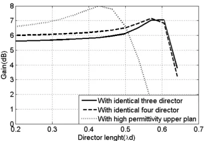
Fig. 6. Gain variation as a function of director length for: staked Yagi with three and four identical directors; Stacked Yagi with three directors and high permittivity plan.
A reflector plane is added to the driver element, the size and the distance of the reflector are optimized. For different spacing between driver dipole and reflector, Fig. 4 shows the gain variation versus the reflector plane size. It is found that the optimum reflecting spacing for the maximum directivity is between 0.15λ0 and 0.25 λ0 as in case of the standard Yagi structure. The gain increases as the size of reflector increases, and this variation becomes less pronounced beyond 1.25λ0. The dimensional ratio of the reflector to the driven element can be somewhere between 2 and 2.6. Compared to the standard Yagi antenna, this ratio is doubled. The variation of the conductivity of the reflector material has also influence, leading to the degradation of bandwidth and/or directivity as observed in [17].
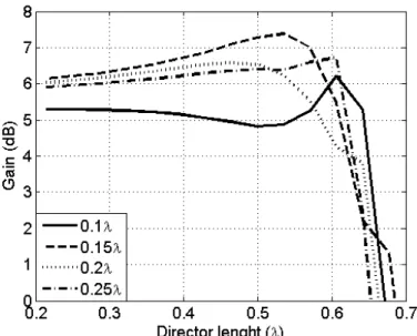
Three directors are added to the dipole and reflector. Fig. 5 shows the variation of the gain with respect to the director length in dielectric for different director-to-director spacing. In this simulated result, the optimum director-to-director spacing is in the order of 0.15λ0 to 0.2λ0, compared with typically 0.2 to 0.35 wavelengths in the design of a standard Yagi. The wavelength in the substrate thickness must be added to obtain the actual spacing. On the other hand, the gain increases with length, and the optimal length of director is around the dipole dimension where the coupling is maximized. A further increase of their size should reduce the array gain rapidly. The dimensional ratio of the director to the driven element can be between 0.8 and 0.95.
As shown in Fig. 6, the gain enhancement is not significant when the fourth director is added, compared to the Yagi antenna with three stacked elements. The addition of an identical fourth director would increase the gain only by 0.25dB. Upper planar substrate with a high permittivity is added in order to reduce the antenna size (footprint) and to increase the gain [19], [20]. Fig. 6 shows the effects of adding this substrate without directors on the antenna gain. An improvement
TABLE II
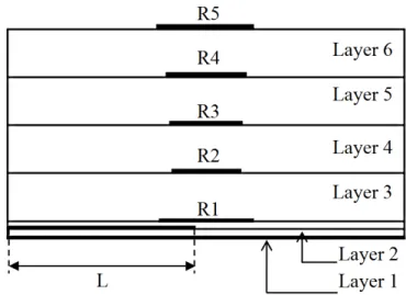
DESIGN 2 FOR PATCH STACKED YAGI ANTENNA
Symbol Value Unity
Ltotal 50 mm Gap 1 0.28 mm Gap 2 14.6 mm R1 9.68 mm R2 4.12 mm R3 7.69 mm R4 6.9 mm R5 7.9 mm TABLE I
DESIGN 1 FOR DIPOLE STACKED YAGI ANTENNA
Symbol Value Unity
W1 1.95 mm W2 5 mm W3 17.25 mm L1 25 mm L2 10.6 mm L3 5.8 mm εr6 10.2 / εr5= εr4= εr3 3.48 / εr2 2.33 / Ltotal 80 mm G1 0.166 λ G2 0.1 λ
of 2 dB can be achieved and the optimal length of the directors becomes shorter. The gain enhancement is given by the following equations [20].
1 2 1 0 1 1 2 8 ⋅ ( ) ≈ ⋅ ⋅ ∆ ⋅ ⋅ n B gain f b n ε λ ε µ (2) in which 1 2 1 1 0 1 2 2 ⋅ = ⋅ ⋅n B⋅ ⋅n b π ε λ ε µ (3) and 2 1 1 1 ( ) 1 (2 / ) tan ( )+ − = + ⋅x f x x π (4)
with B being the thickness of the lower layer andε1,µ1 are its relative permittivity and permeability, respectively. ε2and µ2are the relative permittivity and permeability of the upper layer. n1 = ε1µ1 is the refractive index. ∆ is defined as the frequency deviation parameter.
0
1
∆ = f −
f (5)
where frequency f is near the center frequencyf0.
Composite planar dielectric structures can be used for increasing the directivity of a point source when a resonance condition is established. Particular attention has been given to the physical interpretation of this resonance gain effect in [18]. This is described in terms of leaky waves (LW) excited in the structure. Under certain resonance conditions, a pair of weakly attenuated TE/TM leaky waves becomes the dominant contribution to the antenna aperture field. Equation (2) applied to our specific configuration yields an approximate enhancement of 0.9dB.
A director is added on the upper substrate. Various parameters are optimized starting from the initial value defined in previous paragraphs.The entire structure of design#1 is optimized in order to achieve high gain and large bandwidth at 5.8GHz. Director lengths are perturbed to optimize the return loss with minimum gain loss. The distances between elements along the vertical axis are: G1=0.166λ (8.58 mm) between reflector layer I and driver layer II; G2=0.1λ (5.6 mm) between driver layers II, and director layers III, IV and V.
Fig. 7 shows the influence of elements width on the bandwidth of the design #1. This design can achieve a bandwidth between 6% and 27% at 5.8GHz. It was noticed that this parameter has has the most significant effect when it is selected between 0.05λ and 0.1 λ, and becomes much less influential outside this band. The return loss is more sensitive to the width of the elements
(driver and director) rather than antenna directivity.
The total height of the designed structure is 29mm. Compared with equation (1), it can be observed that the spacing between elements can reduced by a factor of two. The upper director layer is in direct contact with director V. The change of relative permittivity in the interface between the air gap and the substrate results in a higher equivalent relative permittivity, thus reducing the air gap. The size of the stacked substrates is 80x80mm.
Fig.7. S11 as a function of element width.
1.3.2.2 Circular Patch Stacked Yagi Antenna with Dual Polarization (Design #2)
In this design demonstration, the classical dipole is replaced by a patch antenna. The proposed concept offers a possibility to use a wide range of patches instead of the classical dipole as driver. The circular patch has been used as both, a dual polarization feeder, and also an optimization facility, since that is only required to optimize one dimension (radius).
The antenna consists of two substrate layers. The circular patch is etched on the top substrate and the feed lines and ground are etched on the bottom substrate. To achieve the dual polarization the patch is fed by two orthogonal lines. Such a feeding by coupling allows increasing the bandwidth. This patch has a bandwidth of 4.5% at 5.8 GHz. The feed layer (layer I in Fig. 3) is grounded on its bottom side and fed on the other side by 2.26 mm width, 20.27 mm (0.39λ) long strip lines. The feed lines start from the middle of their respective side, and the width is calculated to match the antenna to 50Ω. The circular patch has a radius of 0.187λ (9.68mm) and the spacing between the layers I and II is 0.28mm. The antenna is simulated using Ansoft HFSS
v10, a simulator which makes use of the finite element method.
The proposed circular patch stacked Yagi antenna is shown in Fig. 3. This antenna is designed with the geometry of several layers, and is very similar to the dipole Yagi antenna topology that was described in the above section. In this structure, the Rogers RF/Duroid 5870 substrate is used for all the layers with εr =2.33 and thickness of 0.762 mm (30 mil).
As in the case of the first design, the antenna is optimized to achieve better gain and larger bandwidth, but also the isolation characteristics between the two feed lines must be taken into account.
One constraint of the stacked dipole Yagi antenna is related to its requirement for a large ground plane. Fig. 8 shows the gain enhancement of the patch antenna in connection with the ground size, suggesting that the gain increases with the size of the ground plane. The optimal ratio of the reflector to the driven element is in the order of 1.6, which is comparable to the standard Yagi antenna topology. This antenna can be used to reduce overall dimensions of patch stacked Yagi antenna; a high gain with reduced ground plane can be obtained.
Fig. 8. Gain versus Ground plan size.
Fig. 9 plots the gain versus the number of parasitic elements for adjacent director-to-director spacing of 0.3λ0. Note that adding the sixth director increases the gain only by 0.1dB. Similar to the first design case, the gain performances are generally controlled by the director spacing and director length.
Fig. 9. Gain versus the Number of parasitic elements.
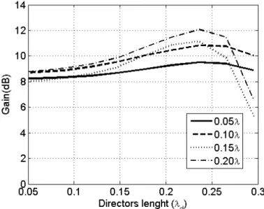
To define initial values, the array is optimized by varying the radius while maintaining the spacing parameters. Fig. 10 shows gain variation versus the element length on dielectric substrate for different director-to-director spacing. The ideal spacing is in the order of 0.2λ0. The ideal radius of the directors should be defined between 0.2λdand 0.24λd. The ratio to the driver patch is the same as in the first design.
Fig. 10. Gain variation with director length for different director-to-director spacing.
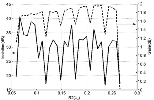
This is followed with the perturbation of different radius starting from the initial value to optimize the bandwidth with smaller gain losses. Maintaining the optimized spacing constant, the reflector spacing radius of the first director (R2)can be used to tune the return loss characteristics
of antenna as well as the isolation between the two polarizations. The effect of variation of the radius on the gain is verified also. As shown in Fig.11, the isolation between the two polarizations have the excursion about 10-15dB for diameter variation in the order of 0.01λd. The effect of diameter variation on the gain is less pronounced as observed in Fig. 11.
Fig. 11. Effect of diameter variation on the gain and on the isolation between the two polarizations.
The optimized patch radius for layers III, IV, V and VI are, respectively, R2=4.12mm (0.08λ), R3= 7.69mm (0.14λ), R4=6.9mm (0.13λ), and R5= 7.9mm (0.15λ).
The size of the layers and the ground plane are 50mm x 50mm. Because of the effective permittivity of substrates that is lower than the previous configuration, the spacing between the directors has increased. Hence, the same substrate has been used throughout the antenna in order to simplify the fabrication process. The vertical spacing between the directors is close to 14.6mm (0.28λ) while the total height of this designed configuration is 60mm.
1.3.3 Results and Discussion
The fabricated prototypes of both antennas are shown in Fig. 12 and 13. The layers are aligned by using four threaded rods with nuts. With this assembly, the gaps between the layers can be easily and precisely controlled.
Fig. 12. Photograph of the first design example for dipole-based Yagi antenna structure.
Fig. 13. Photograph of the second design example for patch-based Yagi antenna structure.
1.3.3.1 The First Design Example
1.3.3.1.1 Transmission Characteristics
S-parameters are measured using Anritsu 37397C Vector Network Analyzer to characterize the transmission properties of the proposed structure over the frequency range of interest. Simulated and measured return losses versus frequency are presented in Fig. 14. It can be seen that the measured center frequency is shifted slightly from the designed target but still very close to 5.8
GHz. The simulation results obtained by HFSS show a good agreement with the measured results. The antenna bandwidth (< -10 dB) covers frequencies from 5.4 to 6.2 GHz or almost 14 % at 5.8 GHz.
Fig. 14. S-parameter characteristics of the prototyped antenna #1. 1.3.3.1.2 Radiation Pattern
Radiation pattern measurement is made in a MI Technology anechoic chamber. Fig. 15 presents calculated and measured co-polar (E plane) radiation patterns. From these results, we can notice a good agreement between the measured and simulated radiation patterns.
It is also observed that the radiation pattern is very directive and symmetric. The 3 dB beam width is approximately 70° for both measured and simulated patterns. The side lobes are very low. The oscillation of the right lobe is due to the mechanical constraints of our anechoic chamber.
Fig. 15. Radiation pattern performances of antenna #1 at 5.8 GHz. 1.3.3.1.3 Antenna Gain
As shown in Fig. 11, the peak antenna gain is about 12 dB based on our simulations and almost 11 dB can be obtained in practice according to our measured results. Although the gain is slightly lower than expected, both curves match very well. The 1 dB drop in measured gain is due to the imperfections of the compact range anechoic chamber used and to losses such as surfaces waves, dielectric losses, and connectors losses (coaxial).
The total height of the designed configuration is 29mm (0.56λ) compared to the designed structure described in [8], which has a dimension of 2.132 λ and uses two more directors to achieve lower gain. Based on equations detailed in [2], the horn antenna is 125mm in length with radiating aperture of 155 by 22.15 mm in order to get a gain of 12dB, and a coaxial to waveguide transition must be added in this case. It is clear that the designed multilayer-stacked Yagi antenna is much more compact than the metallic horn antenna.
1.3.3.2 The Second Design Example
1.3.3.2.1 Transmission Characteristics
Measured and calculated S-parameters of the second antenna are shown in Fig. 16. The measured center frequency for both polarizations (Tx and Rx) is at 5.8 GHz and agrees well with the simulated results. The bandwidth is from 5.6 GHz to 5.85 GHz or 4% at 5.8 GHz, for both
polarizations. The isolation (S21 parameter) between the two ports is nearly 30dB over the entire frequency band, instead of the 25 dB calculated isolation. The bandwidth of this antenna is narrower but sufficient for most LPS or wireless sensor applications at 5.8 GHz. This bandwidth can also be increased by using a wideband patch [21], [22]. The measured performance matches well the simulation prediction. A small difference between the measured and simulated results (S11 is not exactly the same as S22), can be attributed to the fabrication accuracy.
Fig. 16. S-parameter characteristics of the prototyped antenna #2. 1.3.3.2.2 Radiation Pattern
Fig. 17 presents the simulated and measured co-polar (E plane) radiation patterns for the second design. The measured radiation pattern agrees well with the simulated ones. The radiation pattern is again very directive and symmetric. The measured beam width (3 dB definition) is approximately 60 degrees, compared to 70 degrees for the simulated pattern. Both polarization curves are very similar (that is normal because of the symmetry of this structure).
1.3.3.2.3 Antenna Gain
Fig. 17 shows the gain performance based on both simulated and measured results. The respective maximum gain for the simulation and the measurement are 11.66dB and 9.76dB. There is a loss of 1.9dB between the two gains. This loss is due to a frequency shift of the fabricated antenna (a maximum gain of 10.28dB can be reached at the frequency of 5.75GHz), the fabrication tolerance and losses in the measurement circuits.
To achieve a comparable gain, DeJean in [25] proposed a bi-Yagi and quad-Yagi which consist of seven planar patch elements. The size of the ground plane is 1.9 λ x 1.9 λ compared to 1.16 λ x 0.96 λ - the size of our demonstrated antenna.
Fig. 17. Radiation pattern performances of antenna #2 at 5.8 GHz.
1.3.4 Conclusion
In this paper, two classes of novel antenna based on the classic Yagi–Uda antenna concept, have been proposed and demonstrated for the first time theoretically and experimentally. By using multilayer-stacked substrates, these designs allow compact size realization and achieve good performance at the demonstrated frequency of 5.8 GHz.Two different antenna configurations are presented and showcased, one based on dipole for single polarization, and the other on circular patch for dual polarization. The characteristics of such proposed two types of antenna with respect to various parameters such as reflector dimension, director dimension, and spacing between those elements have been studied. The measurement results of S-parameters show a reasonably good bandwidth (a bandwidth of 15% can be reached with the novel structures). And also, the measured radiation pattern performance is very similar to the simulated results. Both designs have a peak gain of about 10dB. Compared to the microstrip array Yagi antenna, which makes use of planar patches, this novel design can yield high gain and also the entire structure is very compact in size by using the vertical dimension. In this case, a large number of directors can be implemented in such multilayered geometries. Based on such new design concepts, many innovative structures with interesting properties can be realized by using different planar patches
in the driver layer, or stacked substrate with zero air gap (especially for high frequency applications such as millimeter-wave or even terahertz frequency ranges). This work suggests that the proposed concept provides light-weight, low-cost, high-performance and full integration solutions for local positioning platforms, wireless sensor systems and radar sensor applications. It can be expected that of those new antennas will provide a very attractive design alterative for a wide range of microwave and millimetre-wave systems.
Acknowledgment
The author wishes to thank J. Gauthier and S. Dube of Poly-Grames Research Center, École Polytechnique de Montreal, in the fabrication and mounting of prototypes.
Financial supports from the NSERC of Canada and Regroupement strategique of FQRNT are greatly appreciated.
References
[1] M. Vossiek, L. Wiebking, P. Gulden, J. Wieghardt, C. Hoffmann and P. Heide, “Wireless local positioning,” Microwave Magazine ,IEEE, Volume: 4 , Issue: 4, pp:77 – 86, Dec. 2003.
[2] W L. Stutzman and G. A. Thiele, Antenna Theory and Design , Second Edition, John Wiley and Sons, 1998.
[3] J. Huang, and A.C. Densmore, ”Microstrip Yagi array antenna for mobile satellite vehicle applications”, IEEE Trans. Antennas Propag., 39, pp. 1024–1030, 1998.
[4] L.C. Kretly and C.E. Capovilla, "Patches driver on the quasi-Yagi antenna: analyses of bandwidth and radiation pattern", Proceedings ofthe International Microwave and Optoelectronics Conference, Sep. Vol. 1, pp: 313-316,
[5] Y. Qian, W. Deal, N. Kaneda, and T. Itoh, “Microstrip-fed quasi-Yagi antenna with broadband characteristics”, Electron. Lett, 34, pp. 2194–2196 , 1998
[6] G. Zheng, A. Kishk, A. Yakovlev, and A. Glisson, “ Simplified feeding for a modified printed Yagi antenna”, IEEE Antennas Propagat Soc Int Symp Dig 3 , 2003, 934–937. [7] Q. Yongxi, and T. Itoh, "Active integrated antennas using planar quasi-Yagi
radiators",Proceedings of the International Microwave and Millimeter Wave Technology Conference, September2000. pp: 1-4.
[8] M. Alsliety, and D. Aloi, ”A low profile microstrip yagi dipole antenna for wireless communications in the 5 Ghz band,” IEEE International Conference on Electro/information Technology, 2006. pp:525-528
[9] J. P. Damiano, J. Bennegueouche, and A. Papiernik, "Study of multilayer microstrip antennas with radiating elements of various geometry," IEE Proceedings, Vol. 137, No. 3, Pt. H, Jun. 1990.
[10] R. Li, G. DeJean, M. Maeng, K. Lim, S. Pinel, M.M. Tentzeris, and J. Laskar, "Design of compact stacked-patch antennas in LTCC multilayer packaging modules for wireless applications," IEEE Trans. Advanced Packaging, vol. 27, issue 4, pp. 581 – 589, Nov. 2004.
[11] H. W. Ehrenspeck and H. Poehler, “A new method for obtaining maximum gain from Yagi antennas,” IRE Trans. Antennas Propagat., vol. AP-7, pp. 379–386, Oct. 1959. [12] P. S. Bhatnagar, J. P. Daniel, K, Mahdjoubi, and C. Terret, "Experimental study on
stacked triangular microstrip antennas", Electronics Letters, Vol. 22, No. 16, pp. 864-865, July 1986
[13] C. Guan-Yu, and Jwo-Shiun, “A printed dipole antenna with microstrip tapered balun”, Microwave and optical technology letters. Vol. 40, No. 4, February 20 2004
[14] N. Michishita, and A. Hiroyuki "A Polarization Diversity Antenna Using a Printed Dipole and Patch with a Hole,” IEICE Trans. Electronics and Communications, Part 1, Vol.86, No.9, pp57-66, 2003.
[15] S. Dey, C.K. Aanandan, P. Mohanan, and K.G. Nair "Analysis of cavity backed printed dipoles", Electronics letters, Vol. 30 No. 3, February 1994.
[16] L. C. Shen, and G. W. Raffoul, “Optimum Design of Yagi Array of Loops”, IEEE Transactions on Antennas and Propagation V, 22, Iss 6, pp:829- 830, Nov 1974
[17] J.A. Nessel, A. Zaman, R.Q. Lee, and K. Lambert, “Demonstration of an X-Band multilayer Yagi-like microstrip patch antenna with high directivity and large bandwidth,”
IEEE International Symposium on Antennas and Propagation & USNC/URSI National
Radio Science Meeting. Washington, DC, July 3–8, 2005, pp: 227-230 vol. 1B.
[18] D.R. Jackson, and A.A. Oliner, ”A Leaky-Wave Analysis of High-Gain Printed Antenna Configuration,” IEEE Trans. Antennas Propagat., vol. 36, n.7, pp. 905-910, July 1988.
[19] A. Hoorfar, “Analysis of a “Yagi-Like” Printed Stacked Dipole Array for High-Gain Application”, Microwave and Optical Technology Letters, Vol.17, No 5, April 5 1998. [20] D. R. Jackson and N. G. Alexopoulos, ‘‘Gain Enhancement Methods for Printed Circuit
Antennas,’’ IEEE Trans. Antennas Propagat., Vol. AP-33,pp. 976-987. , Sept. 1985. [21] S. K Padhi, N. C. Karmakar and C.L. Lawan, “An EM coupled dual-polarized microstrip
patch antenna for RFID applications”, Microwave and optical technology letter, vol. 39, No 5, December 2003.
[22] Antar, Y. M. M., Dajun Cheng, Guozhong jiang, “Wide-band microstrip patch antenna for personal communication”, The 6th IEEE International Conference on Electronics, Circuits and Systems, 1999. Proceedings of ICECS ’99. Volume 3, pp: 1305-1308 vol.3. [23] P.R Grajek, B. Schoenlinner, and G.M Rebeiz, “A 24 GHz high-gain Yagi-Uda antenna
array”, IEEE Trans. Antennas Propag., vol 52, no 5, pp.1257-1261, May 2004.
[24] Gray, D.; J. Lu; D Thiel.; “Electronically steerable Yagi-Uda microstrip patch antenna array”, IEEE Trans. Antennas Propag., vol. 46, pp 605-608, May 1998.
[25] Gerald R. DeJean,“Design and Analysis of Microstrip Bi-Yagi and Quad-Yagi Antenna Arrays for WLAN Applications”,IEEE Antennas and Wireless Propagation Letters, vol. 6, 2007
CHAPITRE 2 ANTENNES À 60 GHZ
2.1 Présentation
Les antennes présentées au chapitre 1 ont montré le fonctionnement à 5.8 GHz du principe utilisé. Il apparaît aussi clairement que ce type d’antenne est adapté pour les fréquences plus élevées car l’espace entre les éléments dans ce cas devient tel qu’aucun espace d’air n’est requis entre les substrats empilés. Cela permet donc d’avoir une structure multicouche compacte et plus facilement fabricable avec les techniques de micro-fabrication. Une première antenne fonctionnant à 60 GHz utilisant une alimentation microstrip a été étudiée, simulée et fabriquée. Suite à ce travail, un réseau d’antennes 4x4 utilisant l’élément précédent et une alimentation GIS [Deslandes et Wu (2006)] a été simulé et réalisé. Le GIS est utilisé afin que le réseau de distribution ne perturbe pas la partie rayonnante du réseau d’antennes. Cela permet une bonne isolation entre les composants étant donné qu’il n’y a pas de rayonnement parasitique. L’antenne peut aussi être mise en cascade avec le démodulateur sans utiliser de transitions car le six-port et l’antenne utilisent la même technologie de guide.
2.2 Article 2 - Very Small Footprint 60 GHz Stacked Yagi Antenna
Array
Olivier KRAMER, Tarek DJERAFI, and Ke WU, Fellow, IEEE
“Very Small Footprint 60 GHz Stacked Yagi Antenna Array”
Soumis dans dans “IEEE Transactions on Antennas and Propagation” le 25 novembre 2010. Manuscript ID AP0903-0249.R2
Abstract—Millimeter wave applications such as short-range high-speed wireless links require modular, compact-size and high-directivity antennas. In this paper, high-gain compact stacked multilayered Yagi designs are proposed and demonstrated in the V-band. This novel design shows for the first time an antenna array of Yagi elements in millimeter wave stacked structure. To demonstrate the proposed concepts and design features, we create a 4x4 antenna array having excellent gain performance as well as very small footprint. A single element stacked Yagi antenna fed with microstrip is studied in order to obtain the desired performance. An analysis is performed to define the structure limitations. Measured results of the fabricated antenna prototypes are in good agreement with simulated results The measured Yagi antenna attains 11 dBi gain over 4.2% bandwidth with a size of 6.5x6.5x3.4 mm3. A 4x4 array of Yagi antenna using an SIW (Substrate Integrated Waveguide) feeding technique is conceived. Both simulated and measured results match with each other very well. The 4x4 array has a size of 50x50x60mm3, and reaches a measured gain of 18 dBi over 7% bandwidth. An alternate configuration of the array using angled Yagi antenna elements allows a significant improvement of the side lobe level (SLL) with a low impact on the gain performances. The proposed antennas are excellent candidates for integrated low-cost millimeter-wave and even terahertz systems. The small foot print, the antenna design flexibility as well as its easy adaptation to automatic fabrication processes are good assets for making short range portable imaging systems.
Index Terms—Array, SIW, microstrip antenna, Yagi-Uda, stacked antenna, circular patch, SLL, feeding network, millimeter-wave and terahertz.
2.2.1 Introduction
he recent trend on the development of millimeter-wave frequencies systems has led to many innovative techniques with their successful demonstrations in different applications. Among those applications, the unlicensed bands around 60 GHz and above provides an opportunity for high-data-rate wireless communications and sensing applications with reduced energy per bit [1]; 77 GHz automotive radar [2]; and 94 GHz imagers and radiometers [3], where a lower profile
array antenna can achieve high gain. Millimeter-wave front-ends necessitate antenna systems with small size, low-power consumption and power-efficiency requirements [4], which should be integrated together with circuits to avoid unnecessary transmission line loss. A low side lobe level (SLL) is another important characteristic parameter that must be controlled to minimize the interferences [5]. This is particularly in line with the emerging worldwide discussion on green information and communication technology (Green ICT) policy and its implementations.
The physical gain saturation of planar antennas and more specifically planar antenna array is defined by Hall [6], and it is limited to circa 35 dBi for a large number of elements with a significant decrease in efficiency [7]. The stacked Yagi-Uda antenna can overcome this limit by using the third dimension. The classical Yagi antenna has been widely successful thanks to its simplicity and customizable high gain [8]-[12]. It consists of basically three-elements: a half-wavelength driver dipole, a longer reflector backing the driver and a director on the other side. Presented in a previous paper [13] is a stacked Yagi antenna working at 5.8 GHz for the purpose of proof-of-concept, stacking together the reflector, the driver, and the directors printed on substrate. However, the usual spacing between parasitic elements of 0.2λ is quite large at 5.8 GHz and imposes air gaps as the substrate would be too thick. This integration issue is naturally solved at higher frequencies like millimeter-wave and beyond where a completely integrated stacked structure can be achieved owe to wavelength comparable with dielectric substrate thickness. Such structures are suitable for multilayer processing techniques including PCB, LTCC and photoimageable thick-film process, which have become more mature in integrated circuit design, fabrication and integration [14][15].
Fig. 1. Proposed circular-patch based Yagi antenna.
First of all, a V-band single antenna element is designed and demonstrated, using six elements fed by microstrip line. An analysis of the dielectric loss as well as the effect of coupling in the structure is performed in order to design the 4x4 planar antenna array. The array makes use of an SIW (Substrate Integrated Waveguide) network in order to feed a 4x4 array by coupling the radiating elements through rectangular slots. The SIW is used to reduce or even suppress the radiation that generally appears in microstrip feeding structure. Hence, it can be connected to a demodulation circuit without interferences. An alternate configuration of the array is also presented. It is composed of Yagi elements oriented in different directions with geometrical offset with respect to each other, allowing for a significant reduction of SLL.
2.2.2 Stacked Yagi Antenna
The general configuration of the stacked Yagi antenna is shown in Fig. 1 and Fig. 2. It is made of one circular patch driver, and four parasitic elements. Of course, other forms of radiating elements can be used instead of circular patch. The antenna respects the same design rules that are used in the conventional dipole based Yagi antenna, except that it is made on stacked planar substrates. The circular patch element offers flexibility of design and optimization without complexity since it requires optimizing one parameter (radius) only and allows the possibility of a dual polarization. By choosing the elements’ diameters, the spacing between them, the substrate
thickness as well as the dielectric constant, the antenna’s performances such as gain, front-to-back ratio, beam width and center frequency, can be modified.
Fig. 2. Side view of the circular- patch based Yagi antenna.
The elements are printed on Duroïd 5880 substrates and have a relative permittivity of 2.2, which reduces spacing between parasitic elements. The spacing is within the standard range which is between 0.15λ and 0.3λ. In this case, the spacing is 0.15λ corresponding to a thickness of 0.508 mm. The radiating element configuration consists of two substrate layers with 0.254 mm of thickness. The circular patch is etched on the top of Layer 2, the feed lines etched on top of Layer 1 and the ground plane at its bottom. The patch is fed by coupling, allowing an increased bandwidth. The proposed stacked dipole Yagi antenna is simulated using Ansoft HFSS v12.0.
Fig. 3 shows the gain as a function of the number of elements in the stacked Yagi structure. It can be noticed that the gain rises steadily when the number of elements increases up to 8-9 elements, then begins to get saturated. Stutzman made a similar curve for classical Yagi antennas and a gain of 12.5 dBi was reached for 10 elements [10]. In our configuration, the gain for the same number of elements is 2 dB more. In addition, the saturation occurs after a higher number of elements. This is due to the fact that the circular patch has more gain than its dipole counterpart, the reflector (here the ground plane of the patch) is four times larger than the radiating elements, and the fact that the air-substrate interface is placed around the antenna confines the electromagnetic fields within the structure. The 0.2 to 0.5 dB of gain drop caused by the dielectric loss shows that it does not have a significant effect on the antenna performances. This is in particular interesting for millimeter-wave integrated antenna-circuit platform based on semiconductor substrates. The optimized dimensions of the prototype antenna are tabulated in