HAL Id: hal-01736110
https://hal.archives-ouvertes.fr/hal-01736110
Submitted on 27 Mar 2018
HAL is a multi-disciplinary open access
archive for the deposit and dissemination of
sci-entific research documents, whether they are
pub-lished or not. The documents may come from
teaching and research institutions in France or
abroad, or from public or private research centers.
L’archive ouverte pluridisciplinaire HAL, est
destinée au dépôt et à la diffusion de documents
scientifiques de niveau recherche, publiés ou non,
émanant des établissements d’enseignement et de
recherche français ou étrangers, des laboratoires
publics ou privés.
Time evolution of the depth profile of 113 defects during
transient enhanced diffusion in silicon
B. Colombeau, N.E.B. Cowern, Fuccio Cristiano, P. Calvo, Nikolay
Cherkashin, Y. Lamrani, Alain Claverie
To cite this version:
B. Colombeau, N.E.B. Cowern, Fuccio Cristiano, P. Calvo, Nikolay Cherkashin, et al.. Time
evo-lution of the depth profile of 113 defects during transient enhanced diffusion in silicon . Applied
Physics Letters, American Institute of Physics, 2003, 83 (10), pp.1953-1955. �10.1063/1.1608489�.
�hal-01736110�
Time evolution of the depth profile of {113} defects during transient enhanced diffusion
in silicon
B. Colombeau, N. E. B. Cowern, F. Cristiano, P. Calvo, N. Cherkashin, Y. Lamrani, and A. Claverie
Citation: Appl. Phys. Lett. 83, 1953 (2003); doi: 10.1063/1.1608489 View online: https://doi.org/10.1063/1.1608489
View Table of Contents: http://aip.scitation.org/toc/apl/83/10
Published by the American Institute of Physics
Articles you may be interested in
Microstructural evolution of {113} rodlike defects and {111} dislocation loops in silicon-implanted silicon
Applied Physics Letters 71, 659 (1997); 10.1063/1.119821
Evidences of an intermediate rodlike defect during the transformation of {113} defects into dislocation loops
Time evolution of the depth profile of
ˆ
113
‰
defects during transient
enhanced diffusion in silicon
B. Colombeaua)and N. E. B. Cowern
Advanced Technology Institute, University of Surrey, Guildford, GU2 7XH, Surrey, United Kingdom
F. Cristiano, P. Calvo, N. Cherkashin, Y. Lamrani, and A. Claverie
Ion implantation group, CEMES/LAAS-CNRS, Toulouse, France
共Received 15 April 2003; accepted 22 July 2003兲
The evolution of兵113其 defects as a function of time and depth within Si implant-generated defect profiles has been investigated by transmission electron microscopy. Two cases are considered: one in which the兵113其 defects evolve into dislocation loops, and the other, at lower dose and energy, in which the兵113其 defects grow in size and finally dissolve. The study shows that dissolution occurs preferentially at the near-surface side of the defect band, indicating that the silicon surface is the principal sink for interstitials in this system. The results provide a critical test of the ability of physical models to simulate defect evolution and transient enhanced diffusion. © 2003 American
Institute of Physics. 关DOI: 10.1063/1.1608489兴
A key issue in modeling and simulation of transient en-hanced diffusion 共TED兲 is the way in which implant-generated extended defects evolve and evaporate during an-nealing, due to the loss of the self-interstitial atoms which they contain. According to conventional TED models,1– 4 self-interstitials are lost from extended defects by emission of single interstitial atoms and their subsequent diffusion to other defects 共Ostwald ripening兲 or to the silicon surface 共dissolution兲. This leads to the notion, verified in process simulators, that the defect band should dissolve preferen-tially on the near-surface side, leading to an increase in mean depth of the band with time. However, it has been reported in recently published transmission electron microscopy 共TEM兲 studies by Moller et al.,5 that the band of 兵113其 defects formed after Si implantation shows no such asymmetric dis-solution. This result has led to considerable controversy in the field, raising the possibility that previous models of point defect transport to the silicon surface are fundamentally in-correct. A resolution of this issue has been an important pri-ority.
In order to get a proper understanding of this phenom-enon we have carried out quantitative TEM studies on the depth profile of 兵113其 defects. We have studied two cases: 100 keV 2⫻1014ions/cm2 Si implantation, leading to the transformation of 兵113其 defects into dislocation loops, and implantation to a somewhat lower energy and dose, 40 keV 6⫻1013ions/cm2 Si, leading to Ostwald ripening and disso-lution of 兵113其 defects without transformation into loops.
The Si implants were performed into Si substrates con-taining lightly doped boron marker layers epitaxially grown by chemical vapor deposition. After implantation, the samples were annealed in nitrogen gas using furnace and/or rapid thermal annealing for various times and temperatures. After processing, plan-view and cross-sectional samples for TEM analysis were prepared by mechanical thinning fol-lowed by ion beam milling. Weak beam dark field imaging
conditions were used to measure the size and depth distribu-tion of the extended defects. Cross-secdistribu-tional共XTEM兲 images were taken from relatively thick共⬃500 nm兲 and flat regions, in order to keep the uncertainty in the defect density mea-surements below 15%. The estimation of the specimen thick-ness was done from Centered Bright/Dark Field images us-ing a 共220兲 reflection. In such imaging conditions the extinction distance, g, is 76 nm. Only specimen areas in which the defect band was entirely included within one thickness fringe were selected for the quantitative analysis. The effect of a 15% defect density variation across the defect band, on the estimated mean depth of the defects, is of the order of 1%.
Considering first the samples implanted at 100 keV 2 ⫻1014 cm⫺2, Fig. 1 shows cross-sectional images of the
de-fect distribution as a function of depth after annealing at 850 °C. For short annealing time, the defect band is
com-a兲Electronic mail: [email protected]
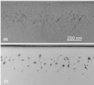
FIG. 1. Cross-sectional images showing the evolution of the defect band after 100 keV Si implantation to a dose of 2⫻1014cm⫺2and annealing at 850 °C. First image共a兲, after a 30 s anneal, shows the presence of only
兵113其 defects, whilst in the second image 共b兲, after 250 s, both 兵113其 defects
and dislocation loops can be found.
APPLIED PHYSICS LETTERS VOLUME 83, NUMBER 10 8 SEPTEMBER 2003
1953
posed of兵113其 defects while after the longer annealing times, these兵113其 defects have evolved and transformed into dislo-cation loops. Plan-view analyses 共not shown兲 indicate that, upon annealing, 兵113其 defects increase in size and decrease in density before their transformation into dislocation loops, while the number of interstitials contained in the extended defects 共total of 兵113其 defects plus dislocation loops兲 de-creases only slightly as a function of time. This behavior, involving growth of large stable defects at the expense of smaller less stable ones, without significant dissolution of the defect band as a whole, is typical of a quasiconservative Ostwald ripening process. The key feature of such a process is that the transport of interstitials between the defects is faster than that to external sinks such as the surface.6
From cross-sectional extraction, Fig. 2共a兲 shows the time evolution of the defect depth distribution at 850 °C. Error bars due to specimen thickness variation共discussed earlier兲 are not reported in the figure, however, they do not affect the following remarks. The defect band remains almost un-changed共in width and peak concentration depth兲 during an-nealing, showing only an overall decrease in defect density, an effect which arises from an increase in the size of the defects during annealing. These results are in perfect agree-ment with the expected defect behavior during a quasicon-servative Ostwald ripening process.
For the case of samples implanted at 40 keV 6 ⫻1013cm⫺2, Fig. 3 shows cross-sectional images
illustrat-ing the time evolution of the defect distribution as a function
of depth, under conditions where兵113其 defects do not evolve into dislocation loops. The processing conditions were Si implantation at 40 keV and a dose of 6⫻1013ions/cm2, fol-lowed by annealing at 740 °C for a range of times. It is immediately apparent that the 兵113其 defects both grow and dissolve, since after annealing for 60 min very few 兵113其 defects can be detected. Plan-view analysis 共not shown兲 clearly shows that upon annealing the兵113其 defects increase in size and decrease in density until they start to dissolve. As a result of the dissolution, the number of interstitials con-tained in the defects decreases dramatically with time.
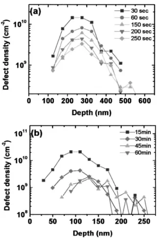
Figure 2共b兲 presents histograms of the depth distribution of the兵113其 defects during time at 740 °C. In contrast to the stable defect band seen in the previously discussed implant, the兵113其 defect band is found to shrink preferentially on the surface side, while the peak of the distribution moves to-wards the right 共from 100 to 125 nm兲. In contrast to the previous data from Moller et al., it therefore appears that the majority of the interstitials escaping from the defect band originate from near the surface side of the band.
The mean depth of the defects, obtained by integrating the defect density over depth, is shown in Fig. 4. The pre-dominant error in the defect density data arises from sam-pling statistics. In this case the 1uncertainty on the mean depth is w/冑N, where w is the standard deviation of the
defect depth profile and N is the number of defects counted. The error bars are 1 values calculated on the assumption that the defect distribution obeys Poisson statistics. In our study the defects are sufficiently large, and their density suf-ficiently low, those errors in counting and locating the de-fects in each image can be neglected in comparison to the sampling. During the time frame of the experiments, the mean depth of the defects formed by the 100 keV 2 ⫻1014/cm2 Si implant remains constant within the
experi-mental errors. However, the mean depth of the defects formed by the 40 keV 6⫻1013 ions/cm2 increases very sig-nificantly with annealing time.
We have seen that the defect bands formed by high dose/ high energy and low dose/low energy implants evolve in dramatically different ways. In the high-dose/high energy
FIG. 2. Time evolution of the defect depth distribution共a兲 after 100 keV Si implantation to a dose of 2⫻1014cm⫺2and annealing at 850 °C, and共b兲 after 40 keV Si implantation to a dose of 6⫻1013cm⫺2and annealing at 740 °C.
FIG. 3. Cross-sectional images showing the evolution and dissolution of the
兵113其 defect band after 40 keV Si implantation to a dose of 6⫻1013cm⫺2 and annealing for共a兲 15, 共b兲 30, 共c兲 45, and 共d兲 60 min at 740 °C.
case, the defect band shows no sign of dissolution during the 兵113其 dominated phase, and subsequent transformation of the 兵113其 defects into loops produces a very stable defect popu-lation that will survive very long annealing times without significant dissolution. In the low dose/low energy case, the ripening of the兵113其 defects is accompanied by rapid disso-lution of the defect band, so that the defects never become large enough to transform into loops.
The reason for the rapid dissolution in the low dose/low energy case is evident from the way in which the band dis-solves. Dissolution occurs first on the near-surface side of the defect band, and only later do the deeper defects start to dissolve as well. The rapid dissolution is evidently a conse-quence of the proximity of the silicon surface, which is a sink for interstitials escaping from the defect band. The ab-sence of dissolution on the deep side of the band shows that interstitials escaping into deeper regions of the silicon en-counter few significant sinks, and most of them simply return to the band to be reincorporated within extended defects. These results perfectly support the view that the surface is the ultimate sink for interstitials escaping from the defect region.
The reason that no significant dissolution is observed on the surface side of the band for the high-dose implant is that the defect density is higher, and the distance to the surface is
larger than in the earlier case. A higher defect density means that it will take longer for a given flux of interstitials to deplete the layer, and the greater depth reduces the gradient, and thus the flux, of interstitials diffusing from the band towards the surface. Before enough interstitials can escape from the band to the surface to produce an observable deple-tion in the near-surface side of the band, the defects have already ripened and transformed into loops, leading to a col-lapse in the interstitial supersaturation, and thus a further huge reduction in the flux of interstitials towards the surface. This does not mean that the band is completely immune to dissolution. What happens is that the time scale for dissolu-tion of the band is increased by several orders of magnitude due to the much greater stability of dislocation loops with respect to dissolution. TED extractions,7 show that even in the high-dose case, the defect band actually does lose some interstitials to the surface. The TED experiments show that the supersaturation of Si interstitials decreases linearly be-tween the defect band and the surface, indicating a flux of interstitials from the band to the surface, as expected.
Clearly our results are in direct contradiction to the con-clusion of Moller et al.,5who found that the defect band does not dissolve preferentially at the surface side. However, the reliability of their result is significantly limited by the fact that they did not measure quantitative depth distributions, but only qualitative estimates of the depth of the top and bottom of the defect band. Such estimates are poorly defined and unreliable, since the defect band does not have well defined edges, see for example Fig. 2. Indeed, only by measuring depth distributions is it possible properly to observe and quantify the shift in the defect profile.
In summary, we have shown that the key factor in the defect evolution is nonconservative Ostwald ripening in the presence of an external sink, clearly identified as the silicon surface. The dissolution appears as a loss of defects on the near-surface side of the defect band, as one would expect when the interstitial supersaturation decreases towards the surface. Finally, our quantitative data on the 兵113其 defect density as a function of depth and annealing time will enable improvement and testing of physical models of defect evo-lution and TED.
This work is part of the IST/FRENDTECH project共IST Project No. 2000-30129兲, and has been supported with an equipment grant from the UK Royal Academy of Engineer-ing.
1D. Lim, C. Rafferty and F. Klemens, Appl. Phys. Lett. 67, 2302共1995兲. 2A. H. Gencer and S. T. Dunham, J. Appl. Phys. 81, 631共1997兲. 3L. Pelaz, G. H. Gilmer, V. C. Venezia, H.-J. Gossmann, M. Jaraiz, and J.
Barbolla, Appl. Phys. Lett. 74, 2017共1999兲. 4
B. Colombeau, F. Cristiano, A. Altibelli, C. Bonafos, G. B. Assayag, and A. Claverie, Appl. Phys. Lett. 78, 940共2001兲.
5K. Moller, K. Jones, and M. Law, Appl. Phys. Lett. 72, 2547共1998兲. 6A. Claverie, B. Colombeau, G. Ben Assayag, C. Bonafos, F. Cristiano, M.
Omri, and B. de Mauduit, Mater. Sci. Semicond. Process. 3, 269共2000兲. 7F. Cristiano, Y. Lamrani, B. Colombeau, P. Calvo, and A. Claverie
共un-published兲. FIG. 4. Time evolution of the mean depth of the defects formed by共a兲 100
keV 2⫻1014cm⫺2 Si implant annealed at 850 °C and 共b兲 40 keV 6 ⫻1013
cm⫺2Si implant annealed at 740 °C. In共a兲 the data are consistent with no changes in the mean depth. In共b兲 the mean depth increases with time. The dotted line is the best straight-line fit to the experimental results.
1955