Any correspondence concerning this service should be sent
to the repository administrator:
[email protected]
This is an author’s version published in:
http://oatao.univ-toulouse.fr/27275
To cite this version: Tan, Reasmey Phary and Rouabhi, Cherif and
Capello, Christophe and Schauber, Julien and Grisolia, Jeremie and
Claverie, Alain and Lachaize, Sebastien and Vieu, Christophe and
Simon, Patrice and Taberna, Pierre-Louis and Guerin, Francois and
Lincelles, Jean-Baptiste and Gessinn, Frederic and Respaud, Marc
Practical Works on Nanotechnology: Middle School to Undergraduate
Students. (2020) IEEE Nanotechnology Magazine, 14 (4). 21-28. ISSN
1932-4510
Official URL
DOI :
https://doi.org/10.1109/MNANO.2020.2994822
Open Archive Toulouse Archive Ouverte
OATAO is an open access repository that collects the work of Toulouse
researchers and makes it freely available over the web where possible
Digital Object Identifier 10.1109/MNANO.2020.2994822
S
Middle school to
undergraduate students.
REASMEY PHARY TAN, CHÉRIF ROUABHI, CHRISTOPHE CAPELLO, JULIEN SCHAUBER, JÉRÉMIE GRISOLIA, ALAIN CLAVERIE, SÉBASTIEN LACHAIZE, CHRISTOPHE VIEU, PATRICE SIMON, PIERRE-LOUIS TABERNA, FRANÇOIS GUÉRIN, JEAN-BAPTISTE LINCELLES, FRÉDÉRIC GESSINN, AND MARC RESPAUDPractical Works
on Nanotechnology
SINCE ITS EMERGENCE A FEW de cades ago, nanotechnology has been shown to be a perfect exam-ple of a crossroad between dif-ferent fundamentals sciences. In the last 10 years, the continu-ous progress of classical top-down lithography and the use of alternative bottom-up elab-oration methods has allowed new and smaller components to be created. Their combina-tion has led to very complex and innovative architectures. At the same time, f lexible, low-cost, and low-ecological-footprint devices have emerged. Thus, the diversity and multi-disciplinary features present chal-lenges in addressing these issues in educational programs.
Practical works are essential for stu-dents, to assimilate the complex theoreti-cal concepts and acquire associated skills. Here, we share our experience of introducing nanotechnologies to university students through practical work. For more than 38 years, we have pro-posed microelectronic-based device-fabrication training that seeks to realize devices in a clean room that is mainly dedicated
to educational purposes. Hereafter, we will describe some brief (two–five days) and practical training in the field of CMOS technology, sensor (gas, strain, and
so on) technologies, or integrated on-chip energy storage. We will focus on the peculiar interest of each practical work, the issues tackled, and organization of the trainings. Finally, we will share our experience in addressing young middle school students.
BACKGROUND
Nanotechnology applications are increas-ingly present in everyday life. If the tre-mendous growth of research topics and the number of publications illustrate an interest in academic research, the routine applications become more present and concern many applications, such as medicine, mechanics, biology, communi-cation, energy, and so on. Electronics are used in all human activities. Downsiz-ing each active element in the integrated circuits has become a key parameter for increasing performances. Thus, due to the necessity of nanotechnology in our life, teaching and training the fundamen-tal concepts used in these applications become mandatory. Therefore, introduc-ing nanotechnology in the pedagogical content becomes more and more chal-lenging. The difficulty arises from the complexity and number of concepts that interact in nanotechnology.
The process requires multidisciplinary knowledge where several fundamental sciences intersect, which can be addressed separately in lectures as a first step. Merg-ing all of these concepts from different disciplines is a challenging task, espe-cially for young, inexperienced students. Therefore, practical works in which each student can elaborate and test his or her own nanodevice are necessary. However, producing nanosized devices or materials often requires dedicated setup and adapt-ed characterization tools, which usually are expensive. Above all, safe laboratory benches and specific infrastructures to
safely manipulate hazardous chemicals and nano-objects are needed.
Our institute, Atelier Interuniver-sitaire de Micro et nano Electronique (AIME), is a French facility connected to the Centre national de la recherche scientifique, two engineering schools and one University Paul Sabatier in Toulouse, France. We are also partnered with the French network dedicated to education in microelectronic and nanotechnol-ogy that is coordinated by the Comité National de Formation en Microélectro-nique (CNFM) (http://www.cnfm.fr). The CNFM brings together 12 plat-forms spread over the country. These platforms are common facilities open to the French educational community as well as foreign universities.
AIME is dedicated to educating and training undergraduate and graduate stu-dents in the fields of microelectronic and nanotechnology. The trainings originally centered on manufacturing and testing silicon (Si)-based semiconductors and microelectronics devices. In the last 20 years, growing interest in nanotechnol-ogy has led us to introduce it into our activities. As such, the trainees fabricate their own devices, starting with a vir-gin Si wafer that will be processed on their own, for all steps of the fabrication process. The contents of these practical works have been defined in close coop-eration with professors and researchers from various universities and engineer-ing schools. These trainengineer-ings provide an experimental view of the fundamental aspects introduced in lectures. Students are introduced to the practical manu-facturing of real nanodevices by fol-lowing the successive fabrication steps, with the appropriate validation proto-cols. Although the experiments typically performed by the students are from a technology transfer from factories and
research laboratories, some are from works published in the literature.
In this article, we report our experi-ence in providing these practical works, especially those focused on nanotechnol-ogy. These training are intimately con-nected to the field of electronics and therefore are based on standard micro-electronic manufacturing procedures that require dedicated facilities (clean rooms) and associated equipment. We will f irst review how the training is generally conducted in a typical work. We then provide some examples of the introduction and manipulation of nano-meter-sized active materials in nanode-vices, in a broad range of applications. To conclude, we present our approach to introducing nanotechnologies to middle school students.
GENERAL WORKFLOWS
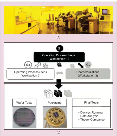
A typical training is provided to a group of up to 18 students for two–five days. The number of manufacturing stages with masking and photolithography (PL) steps, as well as the final electrical tests, define the duration. Therefore, short trainings (two days) involve fab-ricating devices that use less than two masks of PL, which is the case of Si diodes or solar cells, for instance. For longer training (five days), three to five consecutive PLs can be done in pro-cesses such as fabricating microelectro-mechanical systems or MOS transistors. Whatever the duration of the training, our facilities allow students to process a bare Si wafer until the final device, completing all fabrication steps to the final characterization. For this purpose, a 400-m2 clean room is available and equipped for all of the wafer-processing, probe-testing, dicing, and die-packaging steps, as well as for the final test of the device (Figure 1).
For simplicity, let us divide the clean room into three main areas: worksta-tions 1, 2, and 3. A typical schedule depends on the number of students and the length of the training. Typically, the students are split into pairs. For a class of 18 students, this gives us three groups of three pairs (labeled G1, G2, and G3). Each pair of students receives a bare Si wafer to process and one or
Due to the necessity of nanotechnology in our life,
teaching and training the fundamental concepts
used in these applications become mandatory.
several Si wafers dedicated to the parallel characterization (test wafer). The general workflow is depicted in Figure 1(b). The idea is to delay the entrance of G2 and then G3, and to perform a rotation or permutation between all workstations. Workstations 1 and 2 are dedicated to processing the Si wafer, which will give the final device.
For workstation 1, all group manu-facturing processes can be done simul-taneously in parallel by three pairs of students that belong to the same group. In other words, each pair of students uses their own laboratory bench or machine. Each piece of equipment has been tripled: laboratory benches for chemistry opera-tions (wafer cleaning, etching, and so on) or for patterning operations (three masks aligners, three spin coaters, etc.) as depicted in Figure 1(a).
Workstation 2 includes all fabrication steps in which the Si wafers from one group of students are processed simul-taneously. The thermal treatment (such as diffusion, annealing, and oxidation), layers deposition [including metal, oxide, and so on using physical vapor deposition (PVD) or chemical vapor deposited], or equipment that has to be operated by our staff (reactive ion etching, ion-implanta-tion system, semiautomatic wafer prober, dicing, saw, chip bonding, etc.).
Workstation 3 refers to all the char-acterization steps performed on the test wafer. This process allows students to measure the thickness of the layers to estimate the wet etching time, for instance, with different methods (pro-filometry or ellipsometry) or to deter-mine the resistivity of each active layer (before and after doping, metal, and so on) using four-point probe stations. The delay between the groups is voluntarily introduced on day one and is maintained until the last day, when the students per-formed the final test of a single-mounted chip after testing their wafers. This step is primordial, since it allows the trainees to evaluate what they have fabricated on their own with what they have studied in the classroom, particularly through fine characterization of their devices and quantitative analysis.
Although most of the training steps are standardized for microelectronic
device fabrication, they still allow the students to work w it h nanometer-sized materials through the character-ization of the active layers (doped Si/ poly Si or metal, for instance), and by using research laboratory equipment dedicated to the submicronic scale [prof ilometer/atomic force micros-copy, ellipsometer for thickness, and scanning electron microscope (SEM) m icroscopy for obser vat ion]. The same workf low can be used to inte-grate nano-objects as the main active building block of the devices, as will be shown in the next section.
NANO-INSIDE: SI NANOCRYSTAL
INSERTED IN CMOS TECHNOLOGY
The nanocrystal inside training was derived from Grisolia et al.[1] andadapt-ed to our NMOS process. The train-ing consists of fabricattrain-ing a conventional n-MOSFET with a monolayer of Si nano-crystals (NCs) (~3 nm) inserted inside the gate oxide.
This work allows the students to fab-ricate nanodevices that are compatible with CMOS technology, with poten-tial applications such as flash memories. In addition to the standard processes of microelectronic fabrication required for the entire device (four masks and four PLs), the students have the opportu-nity to see how to create and incorporate nanostructures using equipment typical of semiconductor processes. Indeed, the embedded Si nanocrystals are elaborated via low-energy ion implantation (~1 keV) at the Centre d’Elaboration des Maté-riaux et d’Etudes Structurales. By the
G1
G3 G2
Operating Process Steps (Workstation 1)
Operating Process Steps (Workstation 2)
Characterizations (Workstation 3)
Wafer Tests Packaging Final Tests
– Devices Running – Data Analysis – Theory Comparison (a)
(b)
FIGURE 1 (a) The PL area displaying three mask aligners and three laboratory benches. (b) The scheme of our turnover system for an 18-student typical process, from the fabrication pro-cessing to the final test of packaged devices.
end of the training, the students perform the electrical characterization of their devices and demonstrate how electrical charges can be stored (or released) within the Si NCs [Figure 2(c)]. Fundamental physics concepts can be tackled with the students, such as a Coulomb blockade or quantum mechanics.
GAS SENSORS: INTEGRATING
CHEMICALLY SYNTHESIZED
NANO-OBJECTS ON CHIPS
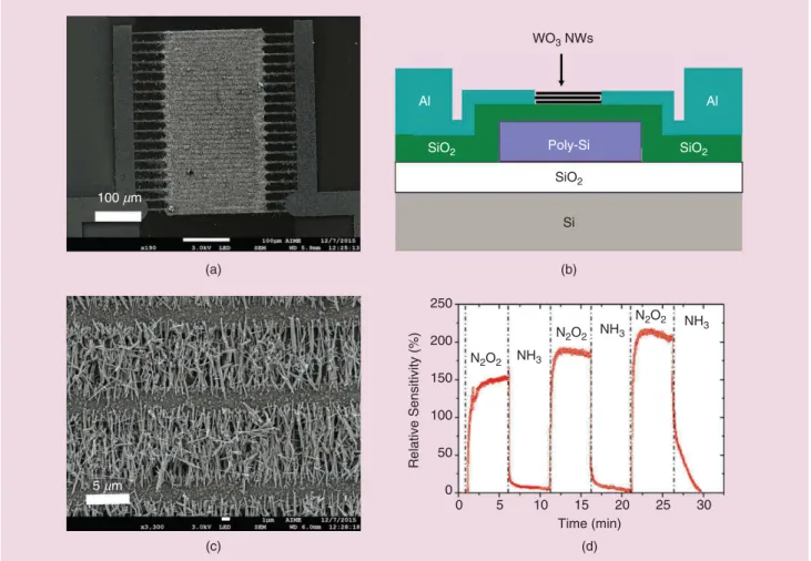
We now present training in which the students produce gas sensor devices by means of standard semiconductor pro-cesses and nanoparticles (NPs) synthe-sized using chemical methods are the active material of the sensor.
NPs can be obtained and integrat-ed into devices by different methods, one of which is the direct growth of the NPs in a localized area, such as with PVD. An alternative is to use the chemi-cal synthesis, which is a facile and cheap route to produce NPs. Then a layer of NPs is deposited on interdigitated combs. Chemical routes allow adapta-tion of the composiadapta-tion, size, and shape
of the NPs, to obtain an optimized surface-to-volume ratio to enhance the sensitivity. If the NP synthesis is straightforward (ease of implemen-tation), especially with our clean room facilities, including NPs in the trainings programs raise several questions, par-ticularly about cross-contamination with other processes, especially with Si-based technology. The second issue concerns the toxicity and safety of the trainees. Besides, localizing the deposit of NPs is still challenging, especially to control the electrical response of the NPs, i.e., to obtain enough percolation paths to ensure a current f lowing through the entire assembly of NPs [2].
To overcome these issues, the NP synthesis takes place in a confined room dedicated to nanomaterial handling that is inside the clean room. WO3 was
cho-sen as the active material since it provides a good sensitivity to gas. It has a low toxicity, and NPs can be easily elaborated following simple experimental proce-dures that are suitable for a training.
Following the general workf low described in the “Background” section,
the students rotate between all worksta-tions, in this case mainly between the chip fabrication and the chemical syn-thesis. A typical sequence is to first fab-ricate the electrodes that will collect the NPs. Two hundred fifty-six chips are created on a 2-in Si wafer. The chips are composed of three types of components: 1) two pairs of interdigitated electrodes (Al); 2) a local heater (doped poly-Si), isolated and buried under an SiO2 layer;
and 3) a thermistor (Al) to measure the local temperature. Additional details of the process can be found in [3].
The geometry of the electrodes has a double function. First, increasing the number of fingers enhances the num-ber of conduction paths. Second, the electrical resistance in NP assemblies are generally high. Thus, increasing the number of channels in parallel low-ers the whole resistance of the array. After fabricating the chips, the stu-dents elaborate their own WO3 NPs,
with the hydrothermal decomposition of tungsten oxide precursors [4], under mild conditions. After 4 h of growth at 180 °C, they obtain needle-shape NPs, namely nanowires (NWs), with a length of 1–2 µm and a diameter of ~100 nm. These N Ws are then deposited on a chip, for which the chip is mounted on a TO5 socket to facilitate handling and electrical addressing.
Dielectrophoresis [5] is used to drive the N Ws between the interdigitated combs. To do so, an ac voltage with a peak-to-peak amplitude of VPP = 20 V
and a frequency of 100 kHz is applied. Under these conditions, the NWs are
SiO2 Si-nc
3 nm
p-Type Si
Source Channel Drain
Gate (Poly-Si) Gate Oxide (SiO2)
ID (mA) Si (p) 0.3 0.2 0.1 0 –2 –1 0 1 2 VGS (V) (c) (a) (b)
FIGURE 2 (a) A cross-section SEM micrograph of the gate oxide showing Si nanocrystals, (b) a scheme of the NMOS fabricated with embedded Si nanocrystals, and (c) the drain current for an oscillating gate voltage (9 V at 100 Hz).
The students perform the electrical
characterization of their devices
and demonstrate how electrical
charges can be stored.
trapped and cover the area between the electrodes [Figure 3(a) and (c)]. The dielectrophoresis optimizes the num-ber of percolation paths between the terminals of the sensors. Finally, dur-ing the last days, the students test their devices in a dedicated homemade setup composed of a sealed chamber. The electrical resistance is measured under subsequent cycles of dried air (N2 and
O2) and other selected gas [NH3 diluted
in N2; for instance, see Figure 3(d)]. The
sensitivity is measured at different local temperatures, thanks to the poly-Si heat-er while the tempheat-erature is controlled with the Al thermistor. WO3 shows an
eff icient response to diluted NH3 at
250 °C.
This training is very rich in terms of educational contents. It provides exam-ples of the cooperative contributions of different fields of science to nanotech-nology, including the chemical synthesis
of NPs, the operating principle of sen-sors, and the use of electric information. The students also learn to characterize nanostructures with specific and adapted tools such as scanning electronic micros-copy. Additional fundamental points can also be taught with their final elec-trical characterizations, including how charge transport is driven in the arrays of nanostructures or how the surface effects become crucial at the nanoscale, par-ticularly how any impurities, voluntarily injected (NH3) or not (surface quality of
the surface of NPs) can modify the con-duction properties in NP assemblies.
MICRO-SUPERCAPACITORS:
CARBON-BASED DEVICES FOR
ENERGY STORAGE
This training addresses the emergent f ield of energy storage in integrated Si devices, particularly the growing demand for mobile applications. A
solu-tion is micro-supercapacitors (micro-SCs) directly integrated onto Si chips. Despite the micrometer size of the structure (Figure 4), the nanoscale technology lies in the working principle of the micro-SC itself and the choice of the active material [Figure 4(b)]. Actually, an SC is based on the charge accumulations of ions provided by an electrolyte between two active electrodes. The capacity den-sity is huge since it relies on subnanome-ter spacing. In addition, we have chosen activated carbon (commercial YP-50F, Kuraray) as active electrodes that present a high density of nanopores (< 2 nm). This high surface specific area material also provides many advantages since it yields high power density (> 10 kW.kg−1), with an almost unlimited life span due to the absence of chemical modifica-tions under charge/discharge cycling. This work has been realized in close col-laboration with research groups from
WO3 NWs Al Al SiO2 SiO2 SiO2 Poly-Si Si 250 200 150 100 50 0 Relative Sensitivity (%) 0 5 10 15 20 25 30 Time (min) N2O2 N2O2 N2O2 NH3 NH3 NH3 100 µm (a) (b) (c) (d) 5 µm
FIGURE 3 The SEM micrographs of the WO3 nanowires trapped between electrodes: (a) large view, (b) a scheme of the device with an integrated isolated polysilicon heater, (c) magnification, and (d) the relative electrical response of the sensor under several N2O2/NH3 cycles.
the Centre Interuniversitaire de Recher-che et d’Ingénierie des Matériaux and represents a technology transfer of their experiments [6].
The first step of the process is dedi-cated to the fabrication of gold (Au) current collectors, which consist of interdigitated electrodes separated by 160 or 220 µm. The patterning of the Au layer requires a single mask. The activated carbon is then deposited by electrophoresis on the Au fingers. For that, the chip is f irst mounted on a TO8 socket and bonded. The mount-ed chip is then dippmount-ed in a solution of YP-50F while applying a dc voltage of amplitude Vdc = 50 V. The chip is then
rinsed in acetone (still under Vdc) to
clean up the device. As can be seen in Figure 4(c), the carbon NPs are only localized on top of the collectors and not between them, preventing any short circuits. Finally, the students character-ize their micro-SCs using a VSP300
(Bio-Logic Instruments) by perform-ing repeated cycles of current measure-ments with NEt4BF4 as an electrolyte.
The micro-SCs give typically 1.2 mF (~5 mF/cm2) depending on the amount of carbon deposited.
This training is less demanding than others that concern the fabrication pro-cesses, but it still offers an overview of a PL/etching process. Its main inter-est lays in the fabrication of a device for mobile and embedded electronic, which is a popular current topic.
NANO AT SCHOOL
This section is dedicated to the training session provided to middle school stu-dents. Allowing young people to have a first concrete experience of nanotechnol-ogy is a major issue considering our tech-nological world and the critical ethical questions that are associated. Motivating young people to pursue scientific careers is another important issue. How do we
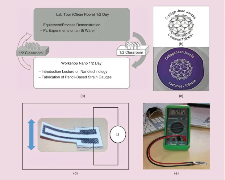
address this topic? We propose a year-long program in their class and a day with practical works in the clean room at AIME. It generally starts with a con-ference and an introductory discussion on the story of micronanotechnology in which the main steps in fundamental science and Si integrated technologies are presented. Their applications for and influence on everyday life are discussed. This work continues all year by introduc-ing some basic concepts in mathematics and physics, but also in history (i.e., the impact of innovation) or literature. For instance, what were their lives anticipated to be like in comparison to ours? Later, a full day is dedicated to visiting AIME and performing practical experiments in the clean room.
The visit is depicted in Figure 5(a). The classroom is divided in two groups with two activities completed in paral-lel. The first is a visit to our clean room and facilities. The standard processes are
Activated Carbon A Collector Electrolyte Spacer + – 0.2 0.15 0.1 0.05 –0.05 –0.1 –0.15 –0.2 0 I (mA) 0 20 40 60 80 100 120 Time (min) (d) (c) (b) (a)
FIGURE 4 A die mounted on a TO8 (a) before and (c) after carbon deposit via electrophoresis [7], (b) a scheme of the operating device [7], and (d) the current measurement as a function of time performed with NEt4BF4 electrolytes.
explained, and some equipment dem-onstrations are performed. To illustrate the use and to show how a nanostruc-ture can be designed on Si, the students perform a PL process on an Si-oxidized wafer capped with an Al layer. For this, they prepare a design, for instance a logo [Figure 5(b)]. Then, AIME’s staff proceeds to the PL step and the final etching of Al [Figure 5(c)] with them. In parallel, the other group attends a practical work focused on nanocar-bon. Students make pencil-based strain gauges on paper [Figure 5(d)], follow-ing the protocol described in [8]. First, the students color a predef ined area with different types of pencils (HB and 3B for instance, with different carbon
contains), and then measure the resis-tance of their gauges with a multimeter [Figure 5(e)]. By bending them upward or downward, they observe a change in resistivity, a decrease and an increase, respectively. A general discussion is then initiated to interpret these experi-mental results. What do they measure? What is the principle of a resistivity measurement? What has been depos-ited? What are the different types of carbon structures (diamond, graph-ite, graphene, nanotube, and fullerene) and their respective properties? Why does the resistance change? What kind of application can be done? What are the advantages and drawbacks of such a technology?
This simple set of experiments is of great interest for many reasons. From a theoretical point of view, we can discuss the resistance measurement based on Ohm’s law, a direct application of their courses. These strain gauges are eas-ily and quickly realized, so the experi-ments can be performed with minimal school furniture although a multime-ter is required. Fundamental questions concerning the innovation, cost reduc-tion, and renewability associated with technologies can therefore be tackled with the middle school students. Sec-ond, by reading the publication, they can have a first view of a typical sci-entific approach (structural properties, microscopy characterization, electrical
FIGURE 5 (a) A general workflow of a practical work (one day) with middle school students. (b) A design proposed by a classroom and (c) its transfer onto an Si wafer. (d) The setup of electrical measurements fabricated and characterized by the students and the (e) graphite-based strain gauges.
Lab Tour (Clean Room) 1/2 Day – Equipment/Process Demonstration – PL Experiments on an Si Wafer
– Introduction Lecture on Nanotechnology – Fabrication of Pencil-Based Strain Gauges
1/2 Classroom 1/2 Classroom
Workshop Nano 1/2 Day
C astanet-Tolosan Col lège Jean Jaurè s (a) (c) (b) Ω (d) (e)
properties, discussion, and so on). Last but not least, this easy experiment can serve as a base to address many pro-spective and emerging fields related to nanotechnologies, such as the use of a f lexible substrate or the introduction of devices based on organic or carbon-derived material.
CONCLUSION
In summary, we have reported some examples of our approach for teaching nanotechnology to students at differ-ent levels ranging from middle school to undergraduate, using experimental works. The aim is to provide insights about nanotechnology, and to develop skills concerning the use of the clean-room facility, micro- and nanofabrication tools, and design of components. The important point is to confront the stu-dents with the “real” world, the use of different machines, and the strict applica-tion of safety rules, particularly regarding the use of dangerous chemicals. These long practical works take up to five days, include numerous fabrication steps, and require concentration and attention. At the end, a critical analysis of the final properties is done in light of the theo-retical models, to assess the successes and difficulties, as well as to provide clues for further improvement.
The main criterion to def ine our practical works always is the safety of the trainees. However, from a practi-cal point of view, the ease of imple-mentation and the reproducibility of the experiments are necessary to reduce the inherent difficulties in experimental works. Our training sessions take place in a clean room with laboratory research facilities. Note that, as shown in the “Nano at School” section, we demon-strate that nanotechnology can also be introduced in trainings with a minimum amount of materials.
Each year, about 600–700 under-graduate and 300–400 middle school students complete one training. New programs are being prepared for a sum-mer school format in which our train-ings will be associated with high-level courses, in the framework of the NanoX graduate school. For perspective, new topics in the fields of microfluidics and
2D semiconducting systems (graphene, MoS2, and so on) are being investigated.
ACKNOWLEDGMENTS
This research was supported by the GIP Coordination Nationale pour la For-mation en Micro-électronique et nano-technologie, France, coordinated by O. Bonnaud from the University of Rennes, France. This study was partially supported by FINMINA grant ANR-11-IDFI-0017 and NanoX grant ANR-17-EURE-0009 in the framework of the Programme des Investissements d’Avenir, France.
ABOUT THE AUTHORS
Reasmey Phary Tan (tan@aime-toulouse .fr) is with the Atelier Interuniversitaire de Micro et Nano Electronique, Institut National des Sciences Appliquées, Uni-versity of Toulouse, France.
C h é r if R o u a b h i (c he r i f @ a i me -toulouse.fr) is with the Atelier Interuni-versitaire de Micro et Nano Electronique, Institut National des Sciences Appli-quées, University of Toulouse, France.
Christophe Capello (capello@aime -toulouse.fr) is with the Atelier Interuni-versitaire de Micro et Nano Electronique, Institut National des Sciences Appli-quées, University of Toulouse, France.
Julien Schauber (schauber@insa -toulouse.fr) is with the Atelier Interuni-versitaire de Micro et Nano Electronique, Institut National des Sciences Appli-quées, University of Toulouse, France.
Jérémie Grisolia (grisolia@ insa -toulouse.fr) is with the Laboratoire de Physique et Chimie des Nano-Objets, Institut National des Sciences Appli-quées, University of Toulouse, France.
Alain Claverie ([email protected]) is with the Centre d’Elaboration des Maté-riaux et d’Etudes Structurales, University of Toulouse, France.
S ébas tien L achaiz e (lacha i ze@ insa-toulouse.fr) is with the Laboratoire de Physique et Chimie des Nano-Objets, Institut National des Sciences Appli-quées, University of Toulouse, France.
Christophe Vieu ([email protected]) is with the Laboratoire d’Analyse et d’Architecture des systèmes, University of Toulouse, France.
Patrice Simon ([email protected] .fr) is with the Centre Interuniversitaire
de Recherches et d’Ingénierie des Maté-riaux, University of Toulouse, France.
Pierre-Louis Taberna (taberna@ ch im ie.ups-t lse) is w it h t he Cen-tre Interuniversitaire de Recherches et d’Ingénierie des Matériaux, University of Toulouse, France.
François Guérin (guerin@aime-toulouse .fr) is with the Atelier Interuniversitaire de Micro et Nano Electronique, Institut National des Sciences Appliquées, Uni-versity of Toulouse, France.
Jean-Baptiste Lincelles (lincelle@ insa-toulouse.fr) is with the Atelier Interuniversitaire de Micro et Nano Electronique, Institut National des Sci-ences Appliquées, University of Tou-louse, France.
Frédéric Gessinn (fgessinn@aime -toulouse.fr) is with the Atelier Interuni-versitaire de Micro et Nano Electronique, Institut National des Sciences Appli-quées, University of Toulouse, France.
Marc Respaud (respaud@insa-toulouse .fr) is with the Atelier Interuniversitaire de Micro et Nano Electronique and the Centre d’Elaboration des Matériaux et d’Etudes Structurales, University of Tou-louse, France.
REFERENCES
[1] J. Grisolia et al., “Nanocrystals inside: Fabrication de composants mémoires MOS à base de nanocris-taux de silicium,” J3eA, vol. 13, no. 0008, pp. 1–7, 2014. doi: 10.1051/j3ea/2014008.
[2] J. Dugay et al., “Room-temperature tunnel magnetoresistance in self-assembled chemically synthesized metallic iron nanoparticles,” Nano Lett., vol. 11, no. 12, pp. 5128–5134, 2011. doi: 10.1021/nl203284v.
[3] C. Rouahbi et al., “Capteur de gaz à base de nanoparticules: Synthèse de nano-objets par voie chimique, intégration et caractérisation de capteurs élaborés en salle blanche,” J3eA, vol. 16, p. 1022, Jan. 2017. doi: 10.1051/j3ea/20171022. [4] X. Wen Lou and H. C. Zeng, “An inorganic route
for controlled synthesis of W18O49 nanorods and nanofibers in solution,” Inorg. Chem., vol. 42, no. 20, pp. 6169–6171, 2003. doi: 10.1021/ ic034771q.
[5] A. Rotaru et al., “Nano-electromanipulation of spin crossover nanorods: Towards switchable nanoelectronic devices,” Adv. Mater., vol. 25, no. 12, pp. 1745–1749, 2013. doi: 10.1002/ adma.201203020.
[6] D. Pech et al., “Ultrahigh-power micrometre-sized supercapacitors based on onion-like carbon,” Nat. Nanotechnol., vol. 5, no. 9, pp. 651–654, Sept. 2010. doi: 10.1038/nnano.2010.162.
[7] R. Tan et al., “Micro-supercapacité à base de car-bone nano-poreux,” J3eA, vol. 16, p. 1021, Jan. 2017. doi: 10.1051/j3ea/20171021.
[8] C. Lin, Z. Zhao, J. Kim, and J. Huang, “Pen-cil drawn strain gauges and chemiresistors on paper,” Sci. Rep., vol. 4, p. 3812, Jan. 2015. doi: 10.1038/srep03812.
![FIGURE 4 A die mounted on a TO8 (a) before and (c) after carbon deposit via electrophoresis [7], (b) a scheme of the operating device [7], and (d) the current measurement as a function of time performed with NEt4BF4 electrolytes](https://thumb-eu.123doks.com/thumbv2/123doknet/2948366.79974/7.892.83.813.592.1088/deposit-electrophoresis-operating-current-measurement-function-performed-electrolytes.webp)