HAL Id: inria-00445943
https://hal.inria.fr/inria-00445943
Submitted on 11 Jan 2010
HAL is a multi-disciplinary open access
archive for the deposit and dissemination of
sci-entific research documents, whether they are
pub-lished or not. The documents may come from
teaching and research institutions in France or
abroad, or from public or private research centers.
L’archive ouverte pluridisciplinaire HAL, est
destinée au dépôt et à la diffusion de documents
scientifiques de niveau recherche, publiés ou non,
émanant des établissements d’enseignement et de
recherche français ou étrangers, des laboratoires
publics ou privés.
On-the-Fly Evaluation of FPGA-Based True Random
Number Generator
Renaud Santoro, Olivier Sentieys, Sébastien Roy
To cite this version:
Renaud Santoro, Olivier Sentieys, Sébastien Roy. On-the-Fly Evaluation of FPGA-Based True
Ran-dom Number Generator. IEEE Computer Society Annual Symposium on VLSI, ISVLSI’09, May 2009,
Tampa, Florida, United States. �10.1109/ISVLSI.2009.33�. �inria-00445943�
On-the fly evaluation of FPGA-based True Random
Number Generator
Renaud Santoro∗, Olivier Sentieys∗ and S´ebastien Roy‡
∗IRISA - University of Rennes {santoro,sentieys}@irisa.fr
‡Dept. of Electrical and Computer Engeneering Universit´e Laval, Qu´ebec, Canada
sebasroy@gel.ulaval.ca
Abstract— Many embedded security chips require a high-quality digital True Random Number Generator (TRNG). Re-cently, some new TRNGs have been proposed in the literature, innovating by their new architectures. Moreover, some of them don’t need to use the post-processing unit usually required in TRNG constructions. As a result, the TRNG data rate is enhanced and the produced random bits only depend on the noise source and its sampling. However, selecting a TRNG can be a del-icate problem. In a hardware context (e.g. Field-Programmable Gate Array (FPGA) or Application-Specific Integrated Circuit (ASIC) implementation), the design area and power consumption are important criterions. To the best of our knowledge, no effective comparison of several TRNGs appears in the literature. This paper evaluates the randomness behavior, the area and the power consumption of the latest TRNGs. These investigations are realized into real conditions, by implementing the TRNGs into FPGA circuits.
I. INTRODUCTION
The objective of a random number generator (RNG) is to produce random binary numbers which are statistically independent, uniformly distributed and unpredictable. RNGs are necessary in many applications like cryptography, com-munication, VLSI testing, probabilistic algorithms, and so on. The number of hardware applications requiring RNGs is continuously increasing, especially in embedded circuits (e.g. Field Programmable Gate Array (FPGA) and Syston-Chip). As a consequence, many applications need an em-bedded RNG. Generally, a hybrid RNG comprising a True Random Number Generator (TRNG) and a Pseudo Random Number Generator (PRNG) is used. PRNGs are based on deterministic algorithms. They are periodic, and must be initialized by a TRNG. TRNGs are based on a physical noise source (e.g. radioactive decay, thermal noise or free running jitter oscillators) and depend strongly on the quality of their implementation.
In cryptography, security is usually based on the randomness quality of a key generated by an RNG. Some PRNGs are recognized to produce high quality random numbers. However, their quality depends in turn on the randomness of the seed, which is provided by a TRNG. PRNG randomness evaluation is usually performed by using a battery of statistical tests. Several such batteries are reported in the literature including Diehard [1] and NIST [2] batteries.
In embedded circuits, two parameters are important, namely
the design area and its power consumption. The dynamic power consumption is proportional to the chip activity and its frequency. TRNG are usually based on a metastable or oscillating signal, implying a large activity and a non negli-gible dynamic power consumption. For the same randomness quality level, the TRNG presenting the smallest area and power consumption should be preferred.
To the best of our knowledge, no effective comparison of several TRNGs appears in the literature. This paper evaluates the randomness behavior, the area and the power consumption of the latest TRNGs. The investigations are realized into FPGA circuits. In order to evaluate the TRNG randomness quality, some statistical tests have been implemented into hardware. As presented in Figure 1, the design analyzes the bit stream produced by each TRNG in real time and in the same external environment conditions. Moreover, experiments on the FPGA temperature and its activity are realized to estimate the repercussions on the TRNG behaviors.
This paper is organized as follows. In Section 2, the digital TRNG selected in the study are described. In Section 3, the TRNG randomness quality is evaluated. In Section 4, the generator area and power consumption are measured. Finally, conclusions and perspectives on the TRNG evaluation are expressed. TRNG TRNG TRNG Hardware statistical tests Results FPGA Temperature variations Fig. 1. TRNG monitoring.
II. DIGITALTRNGSELECTION
As presented in Figure 2, a TRNG can be decomposed into three parts, the physical noise source, the digitization and !000000999 IIIEEEEEEEEE CCCooommmpppuuuttteeerrr SSSoooccciiieeetttyyy AAAnnnnnnuuuaaalll SSSyyymmmpppooosssiiiuuummm ooonnn VVVLLLSSSIII
!777888---000---777666!555---333666888444---222///000! $$$222555...000000 ©©© 222000000! IIIEEEEEEEEE DDDOOOIII 111000...111111000!///IIISSSVVVLLLSSSIII...222000000!...333333
555555
the post processing unit [3]. The digitization and the post-processing outputs are usually called respectively the Digitized Analog Signal (DAS) and the internal random numbers. The post-processing unit is usually required in TRNG construc-tions. Its objective is to correct the imperfections of the DAS. Several techniques are described in the literature, such as the Von Neumann extractor, hash function or randomness extractor. Physical noise source Digitization Noise signal Te das Post-processing Internal Random numbers Fig. 2. TRNG decomposition.
Most of the TRNGs implemented in FPGA or ASIC use phase jitter produced by a free running oscillator or a Phase-Locked Loop (PLL). Jitter is the deviation of a signal from its ideal behavior. Jitter is caused by deterministic noise (power supply noise, cross-talk noise, pink noise) and by random noise (substrate noise, temperature) and strongly depends on the oscillator generator used in the TRNG (usually a ring oscillator or PLL) [4]. In practice, jitter can be influenced by noise external to the FPGA (power supply noise, temperature) and by chip activity. This dependence is a weakness exploitable by submitting the TRNG to hostile environment conditions. Moreover, even if a prototype TRNG is producing high-quality random numbers in a lab setting, the same behavior may not be true for mass-produced replicas [5].
Recently, three TRNGs have been presented in the literature.
TRNG 1 has been proposed by Sunar and al. in [6]. As shown
in Figure 3, the TRNG is based on sampling the phase jitter of many free-running Ring Oscillator (RO). A RO produces a clock signal where the period is a function of the number of inverter gates (N) (always odd) and the gate propagation delay (τp). The period is equal to TRO = 2 × N × τp. In [6], each
RO comprises the same number of gates. The RO outputs are combined by using a XOR tree and sampled at the frequency fCLK = 40 MHz. The sampled bits are then used as input to a
BCH code applied as a resilient function. The TRNG is based on the principle that RO transitions also produce transitions in the XOR tree output. Consequently, if the RO output is sampled close to a transition affected by jitter, the resulting bit is random. [6] decomposes the RO period into time slots and turns the problem into an urn model. The number of ROs required to satisfy a given randomness level is computed. As this number is too large, the number of ROs is reduced and a resilient function is added. As a function of the number of deterministic bit in the XOR tree output, the BCH code is configured. [6] proposes a solution based on 114 ROs of 13 inverters and a [256,16,113]-BCH code.
D Q Clk Resilient function [256,16,113] BCH code Output N 1 p τ 2 RO 1 RO 114 RO XOR tree
Fig. 3. Oscillator sampling proposed by Sunter et al [6].
TRNG 2 has been recently proposed by Vasyltsov and al.
in [7]. Its objective is to increase the data rates of TRNGs based on oscillator sampling. However, using a classical RO is not possible as the jitter accumulation takes too much time. Consequently, [7] introduces the metastable ring oscillator TRNG (META-RO), presented in Figure 4. The circuit can be efficiently put in a metastable state. As a result, entropy is accumulated faster than in a classical RO. The TRNG operation modes are presented in Figure 5. In the metastable step (called MS in Figure 5), the multiplexors disconnect each inverter from the others. This step helps to put the inverter output in a metastable state. Moreover, since each inverter is disconnected from the others, the inverters can be viewed as a set of independent noise sources [7]. Then, in the second step, the inverters are re-connected to each other and form a RO. An oscillating signal is produced on each inverter output. During this step, the oscillating signal is sampled by the CLK!
clock signal. In order to reduce the bias in the TRNG output, [7] uses a simple Von Neumann extractor. [7] has implemented a 5-stage META-RO. The TRNG has been tested according to AIS31 and the FIPS 140-1/2 standard requirement for about 2.5 Mbits/s data rate.
0 1 1 0 0 1 Control clock generator Delay D Q Output bit CLK Din CLK’
Fig. 4. META-RO architecture proposed by Vasyltsov and al [7].
MS CLK
Mode Gener. MS Gener. MS Gener.
Din CLK’
Metastable state
t
Fig. 5. TRNG generation by using the META-RO circuit.
The third generator uses the Galois Ring Oscillators (GARO) and Fibonacci Ring Oscillators (FIRO) principles
introduced in [8]. FIRO and GARO are defined as general-izations of a RO. As usual, the RO is composed of an odd number of inverters. However, the inverters are tied together through a number of XOR logic gates similar to a Fibonacci and Galois configuration of an Linear Feedback Shift Register (LFSR). A GARO is presented in Figure 6. FIRO and GARO are defined by the associated feedback polynomial f(x) = !r
i=0fixi, where f0 = fr = 1. The properties on the
feedback polynomial have been investigated in [8].
1 −
r
f fr−2 f2 f1
output
Fig. 6. Galois ring oscillator.
[9] extends the works presented in [8] by studying the statistical properties of the FIRO and the GARO. Moreover, [8] also presents a method to increase the randomness and the TRNG robustness by using a XOR combination of a FIRO and a GARO, called the FIGARO. FIRO, GARO and FIGARO constitute highly innovative constructions. Their simplicity, efficiency and small area are very interesting for embedded security circuits. In this work, the GARO generator presented [9] has been retained for its efficiency. [9] studies the FIRO and GARO behavior in a special configuration, the restarting mode. Each time a new random bit is required, the FIRO and GARO are restarted in the same initial conditions. Under the hypothesis that, after restarting, the random noise source contains no residual long-term statistical dependencies, the sampled random bits are statistically independent. However, to confirm this hypothesis, the generator must wait a sufficiently long time after having stopped the oscillator [9]. The restarting mode is interesting to decrease the power consumption as the generator is running only when a random bit is required. Moreover, the restart mode is recommended for high-security applications with an on-line testing of true randomness [9].
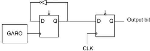
In the present paper, TRNG 3 is the GARO generator. As presented in Figure 7, to produce true random bits, the GARO output is sampled by a D flip-flop at the frequency fCLK. However, to reduce the bias in the sampled output
bits, an intermediate toggle flip-flop is placed between the GARO output and the D-flip-flop. The toggle flip-flop counts the number of 0-1 transitions in the GARO output oscillating signal. The feedback linear polynomial taken for the GARO generator is x31+ x27+ x23+ x21+ x20+ x17+ x16+ x15+
x13+ x10+ x9+ x8+ x6+ x5+ x4+ x3+ x + 1.
To generate a new true random bit, the GARO generator runs in three steps in the restarting mode. In the experiment presented in [9], the generator runs as a classical RO for 60 ns after the restart. Then, the generator is stopped and the flip-flops maintain their states for 40 ns. Finally, the generator
waits 60 ns before restarting a new bit generation. As a result, the TRNG has a data rate of 6.25 Mbits/s. In this work, the same generator has been implemented. In order to implement the same ratio between the three steps, 6 clock cycles have been taken for the first and last stage and 4 cycles for the second.
GARO
D Q
CLK
D Q Output bit
Fig. 7. GARO generator.
The objective of this work is to compare the three selected TRNGs. Their data rates are relatively close, 2.5 Mbits/s for [6] and [7] (in average) and 6.25 Mbits/s for [9]. These data rates have been investigated by the authors in an FPGA context. To compare the TRNG quality, generators are turned to have approximately the same date rate, 2.5 Mbits/s for TRNGs [6] and [9] and up to 2.5 Mbits/s for [7] (in average 1.25Mbits/s).
III. TRNGSTATISTICAL EVALUATION
A. Methodology
In this section, the TRNG randomness is estimated in real conditions. The TRNGs are implemented in an Altera Stratix II EP2S60 development board. As previously stated, TRNGs can be influenced by their external environment and the FPGA activity. Consequently, TRNG robustness must be estimated against variations in both areas. The Altera Stratix II FPGA can be used between −40◦C to100◦C and its recommended
operating temperature is from0◦C to55◦C. Here, TRNGs are
submitted to three different temperature values:25◦C (ambient
temperature),55◦C (the recommended maximal temperature)
and 75◦C. Moreover, TRNG behavior is investigated as a
function of the FPGA activity. Two configurations are tested. The first one is when the FPGA contains only the TRNGs, so there is no activity around the generator. The second configuration consists in artificially creating large amounts of digital activity around the TRNG. Although such a configura-tion should be avoided in practice, it can appear in low-cost embedded security circuits due to size restrictions. The said activity around the TRNGs is realized by using LFSR placed surround the TRNGs.
Several statistical tests exist in the literature to valide ran-dom number generators. Statistical tests are implemented using high-level software programming. When a RNG is evaluated, designers put a huge bit stream into memory and then submit it to software tests. If the bit stream successfully passes a certain number of statistical tests, the RNG is said to be sufficiently random. These batteries are specifically designed for deterministic generators (PRNGs). TRNG validation is
555777
more complicated as generator behavior depend on their con-struction, external environment and essentially on a physical noise source which can differ in practice from ideal noise. However, [3] has described a methodology to evaluate physical generators. The procedure is based on TRNG construction and is the technical reference of AIS 31 [10]. AIS 31 is the German evaluation and certification scheme for TRNG validation. Moreover, one other standard is usually used to estimate the TRNG randomness as recently in [7], namely FIPS 140-1/2 [11].
To evaluate the TRNGs under the same conditions, the generators must be implemented in the same chip. The set of tested parameters calls for the analysis of many TRNG configurations. Moreover, the large number of statistical test realizations required to validate the TRNGs implies the acquire of a huge bit stream collection produced by the generators. Consequently, TRNG analysis via software statistical tests is difficult and is time-consuming. As presented in Figure 1, the proposed methodology is to estimate TRNG quality by using hardware statistical tests. The TRNG monitoring avoids the interfacing problem with an external operating system, as only the statistical tests results must be transferred. However, the hardware tests must be very efficient to be implemented into low-cost embedded circuits and to analyze the TRNG in real time. Moreover, the area occupied by the tests must be insignificant and the test must be placed in the FPGA far enough from the TRNGs to avoid disrupting their behaviors. FIPS 140-2 has been selected. The battery is comprised of the frequency test, the poker test, the run test and the
long-run test. These tests analyze a2 × 104-bit stream. The tests
provide explicit bounds that the computed results must satisfy.
B. FIPS 140-2 implementation
1) Frequency test: This test verifies that the 2 × 104-bit
stream is uniformly distributed. The bias of the sequence is analyzed. The number of 1s (n1) is counted and must lie in
[9726, 10274].
2) Poker test: The bit stream is decomposed into four-bit non-overlapping subsequences and 5 × 10³ blocks are
cre-ated. The poker test verifies that subsequences are uniformly distributed. Occurrences of the 16 possible subsequences are counted. Let ni be the number of occurrences of the integer
i binary representation, with 0 ≤ i ≤ 15. The value of X2
given by X2= 24 5 × 103 "15 # i=0 n2i $ − 5 × 10³, (1) follows a Chi-Square distribution with 15 degrees of freedom and must lie in]2.16; 46.17[ to pass the poker test.
In hardware, computing equation (1) is an area-consuming task. An alternative is to compute the summation!15
i=0n2i and
to compare the result with the required interval
]Ymin, Ymax[. In !15i=0n2i, the maximal value of a counter (ni)
must be computed as a function of the other counter values
i Required interval for n0
i and n1i 1 2343-2657 3 1135-1365 3 542-708 4 251-373 5 111-201 ≥ 6 111-201 TABLE I
RUN TEST REQUIRED INTERVAL.
(nj, j$= i). The optimization problem
max(ni) subject to Ymin<!15j=0n2j< Ymax !15 j=0nj= 5 × 10³ nj≥ 0, 0 ≤ j ≤ 15 (2) must be solved and ni is maximal when !15j=0,j"=in2j is
minimal and the constraints are satisfied. The maximal value of a counter max(ni) is 428. This optimization reduces the
counter bit width and the operator size in the Data-Flow Graph (DFG) as only one9 × 9 multiplier and one 21-bit by 21-bit adder are required.
3) Run test: The run test determines if the number of runs of various lengths is as expected in a random sequence. Let n1
i and n0i be respectively the number of 1-runs (sequence
of consecutive 1s) and 0-runs (sequence of consecutive 0s) of length i. For 1 ≤ i ≤ 6, n1
i and n0i are counted. If the
occurrences satisfy Table I, the random sequence passes the run test. Only twelve counters are required to memorize the occurrence of each run.
4) Long run test: This test verifies that there are no runs of length 26 or more, requiring only a 5-bit counter.
It has been shown in this section that the selected tests need very few arithmetic and memory hardware resources. Consequently, even if the four selected tests are less powerful than a stringent battery such as Diehard, results show that these tests provide a good trade-off between their ability to detect TRNG weaknesses and hardware efficiency. As demonstrated in the next section, the hardware tests have a high operating frequency, allowing the analysis of a TRNG in real-time.
5) Implementation results: Statistical tests have been syn-thesized in a Xilinx Virtex 2 FPGA to compare the design with the implementation presented in [12]. Table II shows the total number of Look-Up Tables (LUT) and the design maximum frequency. In [12], the FIPS 140-2 implementation has been realized. However, the obtained maximal frequency is equal to 113 MHz in a Xilinx Virtex 2 FPGA. Consequently, as shown in Table II, our design is more efficient.
C. Results of the FIPS 140-2 statistical evaluation
The TRNGs and FIPS 140-2 tests have been implemented into an Altera Stratix II EP2S60 FPGA to realize the de-sign presented in Figure 1. For each generator evaluation (FPGA temperature and activity), 500 FIPS 140-2 realizations
targeted FPGA Xilinx Virtex 2 XC2V1000-6 Total LUTs 626 (6%) Maximum 134.7 MHz frequency (MHz) TABLE II
BATTERY IMPLEMENTATION RESULTS INXILINXVIRTEX2.
are applied to analyze a 10M random bits. For each test, the success percentage on the 500 realizations is computed. Figures 8, 9 and 10 show respectively the evaluation results of TRNGs [6], [7] and [9]. The figure x-axis represents the configuration in which the generators are evaluated. The (a), (c) and (e) configurations designate when any surrounding activity is applied around TRNGs and for FPGA temperatures respectively equal to 25◦C, 55◦C and 75◦C. The configurations
(b), (d) and (f) represent the TRNG evaluation when a high activity is applied on the outlines of the generators and for FPGA temperature respectively equal to 25◦C, 55◦C and
75◦C.
As presented in Figure 8, TRNG [6] is practically always declared truly random by the tests, excepted when the FPGA temperature is equal 55◦C and 75◦C and for activity applied on
the TRNG edges ((d) and (f) configurations). In this case, the run test success rate is about 99.4%. However, the variations of the FPGA temperature and the surrounding activity around the TRNG [6] have only small impacts on the generator randomness.
The TRNG [7] randomness evaluation results are presented in Figure 9. As shown, the TRNG is more influenced by the external environmental conditions. For an FPGA temperature equal 25◦C and without activity around the generator ((a)
con-figuration), the generator randomness quality is high, excepted for the long-run test success rate which is equal 89.6%. Then, as shown by the poker and run test results in configuration (b)-(f), the variation of the FPGA temperature and the surrounding activity around the TRNG degrade the generator randomness. Finally, the TRNG [9] evaluation presented in Figure 10 shows that the FPGA temperature variations have few impact on the test results when any activity is surrounding the generator ((a), (c) and (d) configurations). However, when a high activity is applied around the TRNG ((b), (d) and (f) configurations), the frequency test is usually failed by the generator.
After having discussed the TRNG success percentages from the FIPS 140-2, the generator area and power consumption are investigated in the next section.
IV. TRNGAREA AND POWER CONSUMPTION Each TRNG has been implemented in an Altera Stratix II EP2S60 FPGA. The TRNG area is summarized in Table III
a b c d e f 0 10 20 30 40 50 60 70 80 90 100 TRNG configuration Success percentage
TRNG Sunar and al. evaluation
Freq Poker Run Long run
Fig. 8. FIPS 140-2 test success percentage (%) obtained by TRNG [6].
a b c d e f 0 10 20 30 40 50 60 70 80 90 100 TRNG configuration Success percentage
TRNG Vasyltsov and al. evaluation
Freq Poker Run Long run
Fig. 9. FIPS 140-2 test success percentage (%) obtained by TRNG [7].
a b c d e f 0 10 20 30 40 50 60 70 80 90 100 TRNG configuration Success percentage
TRNG Dichtl and al. evaluation
Freq Poker Run Long run
Fig. 10. FIPS 140-2 test success percentage (%) obtained by TRNG [9]. as a function of the ALUT number returned by the Altera Quartus 7.2 software. As presented, the smallest TRNG is [7]. The TRNG consumes only a few ALUTs. TRNG [9] occupies a little more area. On the other hand, TRNG [6] consumes an important number of ALUTs. As a consequence, TRNGs [7] and [9] must be preferred in low-cost embedded security chips. Measuring the TRNG power consumption by using FPGA
555!
TRNG ALUT number
Sunar and al. [6] 1,652
Vasyltsov and al. [7] 9
Dichtl and al. [9] 73
TABLE III
ALUTNUMBER REQUIRED BYTRNGIN AALTERAEP2S60 FPGA.
TRNG Dynamic power (mW)
Sunar and al. [6] 45.359
Vasyltsov and al. [7] 2.52
Dichtl and al. [9] 3.96
TABLE IV
DYNAMIC POWER OF THE THREETRNGIMPLEMENTED IN ANACTEL
IGLOOAGL125V2 FPGA.
constructor tools gives some strange results. The tools seem to have some difficulties to simulate the signal metastabilities. Therefore, we resorted to direct power consumption measure-ments on the FPGA. The Actel Igloo Icicle board makes it possible to measure the FPGA core current and consequently to compute the dynamic power. After having implemented the TRNGs into the low-cost and low-power Actel Igloo FPGA, their dynamic power consumption is measured. Results are presented in Table IV. During the random generation stage, the power consumption of TRNG [6] is larger by a factor of 18 and 11.5 than TRNGs [7] and [9]. The table shows also that the TRNG power consumption of [7] and [9] is close.
V. CONCLUSIONS AND PERSPECTIVES
TRNG statistical properties have been investigated by using statistical tests. The objective has been to evaluate TRNGs un-der homogeneous conditions and to analyze their behavior as a function of the FPGA temperature and activity. The number of TRNG configurations and the number of tested TRNGs make the acquisition of random bits difficult. Consequently, the proposed methodology has been to use a hardware version of a proven and recognized battery of statistical tests, the FIPS 140-2 standard. The FIPS 140-140-2 makes TRNG analysis possible in real time. Its efficiency makes it permits to implement many batteries in the same chip. As a result, the TRNGs can be evaluated into the same FPGA.
Experiments have shown that TRNG [6] seems to be more random and robust than the two others. For almost all TRNG external conditions, the FIPS 140-2 success percentages are close to 100 %. The success percentages of TRNG [7] and [9] are high when the FPGA is used at25◦C and without activity
around the generators. However, the TRNG [7] randomness is damaged when the FPGA is used at55◦C and75◦C and when
activity is applied around the generator. In contrast, the TRNG [9] is less sensitive to the FPGA temperature variation. Never-theless, the activity applied around the generator damages the generator performance.
However, in TRNG [9], the random bit stream is directly produced by the sampled noise source. On the contrary, [7]
and [6] apply a post-processing unit on the sampled noise source to reduce the defects produced by the generators. [7] uses a very basic decorrelator, the Von Neumann extractor. [6] applies a more complicated transformation. The transformation can hide some TRNG weaknesses [3]. In AIS 31, TRNGs are divided into two functionality classes, P1 and P2. A TRNG is said to belong to P1 [10] if the internal random numbers pass a certain number of statistical tests described in [3]. P1-TRNGs are not sufficiently secure for applications such as session key generation, signature key pairs or signature parameters [5]. Consequently, the more restrictive P2 class has been introduced. In P2-TRNGs, the digitized analog signal is also tested. In this study, only the randomness of the internal random bits produced by TRNGs have been investigated. In a future work, the objective is to estimate the digitized analog signal randomness by implementing the AIS 31 statistical tests in an FPGA. As a result, the TRNG random noise source property could be evaluated and compared.
Finally, the TRNG area and power consumption have been investigated in practice. The area of TRNG [6] is larger than the two others and its power consumption is upper by a factor 18 and 11.5 than TRNGs [7] and [9]. TRNG [7] and [9] area and power consumption are close.
REFERENCES
[1] G. Marsaglia, “Diehard: A battery of tests of randomness,” Florida State University, Tallahassee, FL, USA, Tech. Rep., 1996. [Online]. Available: http://stat.fsu.edu/pub/diehard/
[2] A. Rukhin, J. Soto, J. Nechvatal, M. Smid, and D. Banks, “A statistical test suite for random and pseudorandom number generators for statistical applications,” NIST Special Publication in Computer Security, pp. 800– 22, 2001.
[3] W. Killmann and W. Schindler, “A proposal for: Functionality classes and evaluation methodology for true (physical) random number gener-ators,” T-Systems debis Systemhaus Information Security Services and Bundesamt f¨ur Sicherheit in der Informationstechnik (BSI), Tech. Rep., 2001.
[4] A. M. Fahim, Clock Generators for SOC Processors: Circuits and Architectures (Text, Speech & Language Technology). Secaucus, NJ, USA: Springer-Verlag New York, Inc., 2005.
[5] W. Schindler and W. Killmann, “Evaluation criteria for true (physical) random number generators used in cryptographic applications,” in CHES ’02: Revised Papers from the 4th International Workshop on Crypto-graphic Hardware and Embedded Systems. London, UK: Springer-Verlag, 2003, pp. 431–449.
[6] B. Sunar, W. J. Martin, and D. R. Stinson, “A provably secure true random number generator with built-in tolerance to active attacks,” IEEE Trans. Comput., vol. 56, no. 1, pp. 109–119, 2007, member-Berk Sunar. [7] I. Vasyltsov, E. Hambardzumyan, Y.-S. Kim, and B. Karpinskyy, “Fast digital trng based on metastable ring oscillator.” in CHES, ser. Lecture Notes in Computer Science, E. Oswald and P. Rohatgi, Eds., vol. 5154. Springer, 2008, pp. 164–180.
[8] “New methods for digital generation and postprocessing of random data,” IEEE Trans. Comput., vol. 55, no. 10, pp. 1217–1229, 2006, member-Jovan Dj. Golic.
[9] M. Dichtl and J. D. Golic, “High-speed true random number generation with logic gates only,” in CHES, 2007, pp. 45–62.
[10] “Ais 31: Functionality classes and evaluation methodology for physical random number generators. version 1 (25.09.2001),” Tech. Rep., 2001. [11] FIPS, “Security requirements for cryptographic modules, FIPS PUB
140-2,” p. 58 pages, 1999.
[12] A. Hasegawa, S.-J. Kim, and K. Umeno, “Ip core of statistical test suite of fips 140-2,” Communications Research Laboratory and ChaosWare, Inc., Tech. Rep., 2003.
![Fig. 3. Oscillator sampling proposed by Sunter et al [6].](https://thumb-eu.123doks.com/thumbv2/123doknet/12224121.317803/3.918.500.812.106.218/fig-oscillator-sampling-proposed-sunter-et-al.webp)
![Fig. 8. FIPS 140-2 test success percentage (%) obtained by TRNG [6].](https://thumb-eu.123doks.com/thumbv2/123doknet/12224121.317803/6.918.516.782.109.338/fig-fips-test-success-percentage-obtained-trng.webp)
