HAL Id: hal-00686006
https://hal.inria.fr/hal-00686006v2
Submitted on 10 Apr 2012
HAL is a multi-disciplinary open access
archive for the deposit and dissemination of
sci-entific research documents, whether they are
pub-lished or not. The documents may come from
teaching and research institutions in France or
abroad, or from public or private research centers.
L’archive ouverte pluridisciplinaire HAL, est
destinée au dépôt et à la diffusion de documents
scientifiques de niveau recherche, publiés ou non,
émanant des établissements d’enseignement et de
recherche français ou étrangers, des laboratoires
publics ou privés.
Bound the Peak Performance of SGEMM on GPU with
software-controlled fast memory
Junjie Lai, André Seznec
To cite this version:
Junjie Lai, André Seznec. Bound the Peak Performance of SGEMM on GPU with software-controlled
fast memory. [Research Report] RR-7923, INRIA. 2012. �hal-00686006v2�
ISSN 0249-6399 ISRN INRIA/RR--7923--FR+ENG
RESEARCH
REPORT
N° 7923
March 2012 Project-Team ALFBound the Peak
Performance of SGEMM
on GPU with
software-controlled fast
memory
RESEARCH CENTRE
RENNES – BRETAGNE ATLANTIQUE
Campus universitaire de Beaulieu 35042 Rennes Cedex
Bound the Peak Performance of SGEMM on
GPU with software-controlled fast memory
Junjie Lai, André Seznec
Project-Team ALF
Research Report n° 7923 — March 2012 — 11 pages
Abstract: In this paper, we studied the NVIDIA GPU architecture characteristics concerning the SGEMM routine and the potential peak performance of SGEMM on Fermi GPU. Guiding by the analysis, our SGEMM routine achieved about 11% (NN), 4.5% (TN), 3% (NT) and 9% (TT) better performance than cublas in CUDA 4.1 package for large matrices on GTX580 Fermi Card. We also described how to use native assembly language directly in the CUDA runtime source code. Key-words: GPGPU, Fermi GPU, Kepler GPU, Performance Upperbound, Assembly
Bound the Peak Performance of SGEMM on GPU with
software-controlled fast memory
Résumé : Dans ce rapport,nous avons étudié les caractéristiques de NVIDIA GPU architecture concernant la routine SGEMM et la potentiel performance de SGEMM sur Fermi GPU. Guidage par l’analyse, notre routine SGEMM atteint environ 11% (NN), 4.5% (TN), 3% (NT) et 9% (TT) de meilleure performance que cublas dans CUDA 4.1 pour les grandes matrices sur GTX580 Fermi carte. Nous avons également décrit comment utiliser le langage assembleur natif directement dans le code source de CUDA runtime.
Bound the Peak Performance of SGEMM on GPU with software-controlled fast memory 3
1
Introduction
It seems that Moore’s law is still alive for GPU. Nowadays, vendors can still put more computing cores per die and the GPU architecture is evolving rapidly. Fermi GPU is the present generation of NVIDIA GPU. We can find many articles about optimizing specific kernels on Fermi. However, since the architecture is changing very quickly, within a few months (the Kepler GPU is about to come), we may need to repeat the same work again. It would be interesting to generalize our present experience, find the critical architecture parameters, and bound the potential peak performance of those kernels. Hence, with these knowledge, it would be easier for us to move to the newer architecture.
In the report, we chose the GEMM kernel as our example (since we can only access the GTX580 Fermi card, so just SGEMM is evaluated). There are already a few articles about optimizing GEMM kernels on Fermi GPU [5] [6], and also auto-tuning framework is also presented [2]. We want to generalize the bounding factors for this computation-bound kernel and hope this knowledge can profit future optimization work on NVIDIA GPUs. Using the native assembly language to implement the device kernels, the four peak SGEMM performances (4800x4800 matrices) that we have achieved are 1165 GFLOPs (NN), 1157 GFLOPs (TN), 1173 GFLOPs (NT) and 1163 GLOPs (TT), which are 11% (NN), 4.5% (TN), 3% (NT) and 9% (TT) better cublas from CUDA 4.1 (released in Jan. 2012) respectively. Although the result is better than cublas, we have to see that the highest performance of 1173 GFLOPs (NT) is still only about 73.2% of the theoretical peak performance of our GTX580 card (1566KHz shader clock and 1604GLops theoretical peak performance).
2
GPU Architecture Characteristics Concerning SGEMM
2.1
General Architecture Difference between Fermi and GT200 GPU
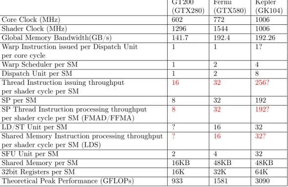
The most obvious improvement from GT200 to Fermi GPU is that the SP number doubles, from 240 (GTX280, 65nm) to 512 (GTX580, 40nm). Each SM in Fermi GPU consists of 32 SPs instead of 8 SPs. For GTX280, each SM has 16KB shared memory and 16K 32bit registers. In GTX580, shared memory per SM increases to 48KB and the 32bit register number is 32K. However, if we consider the resource per SP, the on-die storage per SP actually decreases.
Also for Fermi instruction set, there is a hard limit of maximum 63 registers per thread (for GT200 generation the limit is 127 registers per thread) since in the instruction coding, only 6 bits are left for one register. To reduce the effects of register spilling, Fermi GPU introduces L1 cache. Local writes are written back to L1. Global stores bypass L1 cache since multiple L1 caches are not coherent for global data.
L2 cache is also introduced in Fermi and could reduce the penalty of some irregular global memory accesses. A comparison between GT200 GPU and Fermi GPU is listed in Table 1.
2.2
Necessity of Register Blocking
In this work, we define a warp instruction as the same instruction shared by 32 threads in the same warp, and a thread instruction as the instruction executed by one thread. So a warp instruction launches 32 operations or consists of 32 thread instructions.
In GT200 generation, the scheduler can issue one warp instruction per core cycle and since there are 8 SPs per SM, SPs need 4 shader cycles, or 2 core cycles to process one warp instruc-tion. Apparently, the issuing throughput is higher than the SP’s processing throughput. That is why NVIDIA introduces the concept of dual-issue which means that the scheduler can use the RR n° 7923
4 Lai & Seznec GT200 Fermi Kepler (GTX280) (GTX580) (GK104)
Core Clock (MHz) 602 772 1006
Shader Clock (MHz) 1296 1544 1006
Global Memory Bandwidth(GB/s) 141.7 192.4 192.26 Warp Instruction issued per Dispatch Unit 1 1 1? per core cycle
Warp Scheduler per SM 1 2 4
Dispatch Unit per SM 1 2 8
Thread Instruction issuing throughput 16 32 256?
per shader cycle per SM
SP per SM 8 32 192
SP Thread Instruction processing throughput 8 32 192?
per shader cycle per SM (FMAD/FFMA)
LD/ST Unit per SM ? 16 32
Shared Memory Instruction processing throughput ? 16 32?
per shader cycle per SM (LDS)
SFU Unit per SM 2 4 32
Shared Memory per SM 16KB 48KB 48KB
32bit Registers per SM 16K 32K 64K
Theoretical Peak Performance (GFLOPs) 933 1581 3090 Table 1: Architecture Evolution
’free cycles’ to issue other instructions to corresponding functional units, like SFU. The theo-retical peak performance for arithmetic instructions is calculated as the sum of SPs’ and SFUs’ performance.
However, in Fermi GPUs, SM are redesigned with 2 warp scheduler equipped with a dispatch unit, and 32 SPs. Each warp scheduler issue instructions to 16 SPs. With an issue rate of one warp instruction per core cycle, the scheduler’s or dispatcher unit’s ability could be fully utilized by SPs. The theoretical peak performance for math instructions comes from the SPs’ performance. Also, the percentage of other instructions becomes an issue since if there are too many other kinds of auxiliary instructions like LD/ST, the scheduler doesn’t have enough cycles to issue useful instructions like FFMA.
NVIDIA just launched the new Kepler GPU with 192 SPs on new designed SM or SMX. Now each SMX has 4 warp scheduler, each of which has 2 dispatch unit. And there is no shader cycle, all the units on die run at the core cycle. The hardware details are barely disclosed by now. Let us suppose that the dispatch unit’s ability is the same as before, that is one warp instruction per core cycle. Then each core cycle, the dispatch units can supply 256 thread instructions. Clearly, if the 192 SPs all run at twice the core clock, there won’t be enough instructions to feed them.
A comparison of the three generations of NVIDIA GPUs is listed in Table 1 and the data with a ? is not obtained or speculated.
For Fermi GPUs, according to the disassembly output of cuobjdump, data from shared mem-ory cannot be used as operands of arithmetic instructions like FFMA. The instruction LDS is needed to first load data from shared memory to register and then math instructions can operate register operands. In the worst case, without register reuse, 2 LDS instructions are needed to fetch data for 1 FFMA instruction. So around 1/3 of the instructions devote to FLOPs. Also because the issuing power is not high enough, we can achieve less than 1/3 of the theoretical Inria
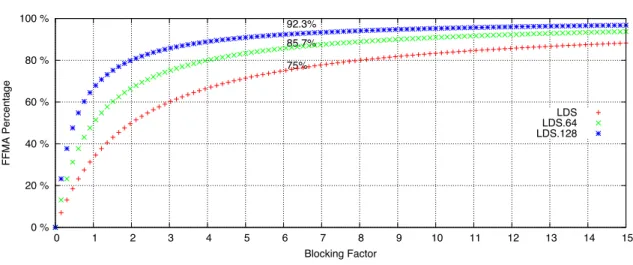
Bound the Peak Performance of SGEMM on GPU with software-controlled fast memory 5 0 % 20 % 40 % 60 % 80 % 100 % 0 1 2 3 4 5 6 7 8 9 10 11 12 13 14 15 FFMA Percentage Blocking Factor 75% 85.7% 92.3% LDS LDS.64 LDS.128
Figure 1: FFMA instruction percentage in SGEMM main-loop with different Blocking Factors peak performance.
Blocking is a well known technique to better utilize memory hierarchy for scientific programs [3] [4]. With different blocking factors of registers, we illustrate the percentage of FFMA in-structions in Figure 1. For example, if 6*6 register blocking is used on Fermi GPU, 75% of the instructions in the main loop of SGEMM are FFMA instructions. In this case, 6*6 registers are needed for C sub matrix per thread and 7 or more registers are needed for one line of A and B matrices per thread. Detailed analysis is in Section 4.1.
2.2.1 Bound performance upperbound DO { Address_Calculation ( ) ; Prefetch_A_GlobalMem ( ) ; Prefetch_B_GlobalMem ( ) ; LDS_A_SharedMem ( ) ; LDS_B_SharedMem ( ) ; FFMA_C_A_B( ) ; __syncthreads ( ) ; STS_Prefetched_A ( ) ; STS_Prefetched_B ( ) ; __syncthreads ( ) ; }
While (ADDR_B < LOOP_END)
Listing 1: GEMM Main Loop Pseudocode
The main loop of the SGEMM routine with prefetching is illustrated in Listing 1. At each iteration, first addresses of A, B are recalculated according to the stride; second, start to load the RR n° 7923
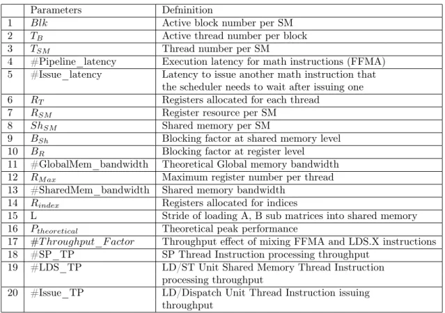
6 Lai & Seznec Parameters Defninition
1 Blk Active block number per SM 2 TB Active thread number per block
3 TSM Thread number per SM
4 #Pipeline_latency Execution latency for math instructions (FFMA) 5 #Issue_latency Latency to issue another math instruction that
the scheduler needs to wait after issuing one 6 RT Registers allocated for each thread
7 RSM Register resource per SM
8 ShSM Shared memory per SM
9 BSh Blocking factor at shared memory level
10 BR Blocking factor at register level
11 #GlobalMem_bandwidth Theoretical Global memory bandwidth 12 RM ax Maximum register number per thread
13 #SharedMem_bandwidth Shared memory bandwidth 14 Rindex Registers allocated for indices
15 L Stride of loading A, B sub matrices into shared memory 16 Ptheoretical Theoretical peak performance
17 #T hroughput_F actor Throughput effect of mixing FFMA and LDS.X instructions 18 #SP_TP SP Thread Instruction processing throughput
19 #LDS_TP LD/ST Unit Shared Memory Thread Instruction processing throughput
20 #Issue_TP LD/Dispatch Unit Thread Instruction issuing throughput
Table 2: Architecture and Algorithm Parameters
A, B data for next iteration into registers; third, load data from shared memory and accumulate to C; after a barrier, store the prefetched data into shared memory.
In our analysis, the L1 and L2 cache don’t devote to the peak performance. L1 cache is not coherent for different SMs and just reduces the latency of accessing some local data. For L2 cache, since the executing sequence of different C sub matrices cannot be controlled by software and if we consider that after some cycles, the blocks executing on different SMs are computing C sub matrices from random positions, there will be little chance for different SMs getting a hit in L2 cache.
To make sure that there are enough threads per SM, equation 1 needs to be satisfied. Equation 4 is the loose condition for register locking factor. B2
Ris the register needed to hold C sub matrix,
BRis one line of A or B sub matrix, and at least another register is needed to load from one line
of B or A sub matrix. Equation 7 is the tense condition for register blocking factor. If we want to prefetch data, at least 2∗√TB∗BR∗L
TB registers are needed. And we also need a few registers to
store the address of matrices in global memory and shared memory.
pTB∗ B2R∗ Lis the size of a prefetched sub matrix for A or B. Equation 5 guarantees that
it is easy to program the prefetching. TSM ≥ 32 ∗
#P ipeline_latency
#Issue_latency (1)
RT ≤ RM ax (2)
Bound the Peak Performance of SGEMM on GPU with software-controlled fast memory 7 TSM∗ RT ≤ RSM (3) B2R+ BR+ 1 < RT (4) (pTB∗ BR∗ L)%TB= 0 (5) Blk ∗ 2 ∗pTB∗ BR∗ L ≤ ShSM (6) BR2 +2 ∗ √ TB∗ BR∗ L TB + BR+ 1 + Rindex≤ RT (7) BSh= q TB∗ BR2 (8)
#T hroughput_F actor = f(BR, #Issue_T P, #SP _T P, #LDS_T P ) (9)
PM emBound= #GlobalM em_bandwidth ∗ BSh (10)
PSM Bound= B2 R B2 R+ BR∗ 2 ∗ #T hroughput_F actor ∗ Ptheoretical (11)
Ppotential= min(PM emBound, PSM Bound) (12)
The #Throughput_Factor is a function of register blocking factor, throughput of SPs, LD/ST units and dispatch units. The function f for Fermi GPU is illustrated in Figure 1 and Figure 2. For Fermi GPU, because of the hard limit of 63 registers per thread, according to the loose condition 4, the maximum register blocking factor is 7. Considering prefetching and using the tense condition 7, the maximum factor is only 6. The detailed register allocation is illustrated in Section 4.1. With this register blocking factor, the register resource per SM can support up to 512 threads. Using equation 5 and 8, we choose 256 threads per block to maximize shared memory blocking factor.
With a 6 register blocking factor, mixing LDS or LDS.64 with FFMA instructions, can both achieve close to 32 thread instructions per shader clock per shader. While using a LDS.64 tion can increase the FFMA instruction percentage to 85.7% from 75%. Though LDS.128 instruc-tion can provide higher percentage of ’useful’ instrucinstruc-tions, the instrucinstruc-tion processing throughput is too low.
According to equation 10, 11 and 12, the performance is bounded by SM’s processing through-put, and the potential peak is about 85% of the theoretical peak performance for SGEMM. And the main limitation factor comes from the nature of Fermi instruction set and the limited issuing throughput of schedulers.
Kepler GPU (GTX680) has already been released. The underlying architecture is different from Fermi GPU. However, our analysis method is still applicable to the new architecture. Since we do not own a new Kepler GPU card, we can only speculate some characteristics of Kepler. From unconfirmed information, the Kepler’s instruction set is similar to Fermi GPU instruction set. That means that the limit of 63 registers per thread still exists. Thus, 6 register blocking is also applicable. And the register resource can support 1024 active threads per SM. The shared memory size can guarantee a blocking size around 96. Thus the main memory bandwidth is RR n° 7923
8 Lai & Seznec not bound. From section 2.2, we speculate that the issuing power of the dispatch units can support both SPs and LD/ST units running at full speed. However, since the FFMA/LDS.X ratio is 3:1 using LDS instructions, SPs may not work in full power (32 ∗ 3 = 96). And using LDS.64 or LDS.128 instruction is not helping since they cannot increase the throughput to shared memory. To sum up all these factors, we speculate that the limitation factor for Kepler GPU to implement SGEMM would be the limited number of LD/ST units and SGEMM’s potential peak performance is the only half of theoretical peak performance. So less than 50% of the theoretical peak performance on Kepler GPU is achievalbe for SGEMM and the key is to reduce the accesses to shared memory. Apparently, Kepler GPU is born for gaming instead of general computing. Other optimization methods are very similar to Fermi GPU.
3
Using Native Assembly Code in CUDA Rumtime Api
Source Code
According to public materials, cuda binary file cannot be directly used in a project built with CUDA runtime api. The .cubin file can only be used with CUDA driver api. We find that loading .cubin file at runtime may degrade the performance. (We still need to look into that.) Besides, a lot of projects are programmed with CUDA runtime api. That restricts the usage of the code written in assembly language.
We managed to integrate our .cubin code into a CUDA runtime project. Since NVIDIA never promises to support this, the method is not guaranteed to be working on future CUDA toolkit. The CUDA binary is generated using an assembly tool for Fermi GPU called Asfermi [1];
1. Add -v -keep to nvcc options, so that all the intermediate files are saved and we can have all the compiling steps.
2. Write one .cu files, eg. kernel.cu, which has one dummy kernel function with the same device function name as your CUDA binary code.
3. Add kernel.cu into the project.
4. Make the project and collect all the compiling command line.
5. Replace the generated kernel.cubin with the one that you implement. Regenerate the ker-nel.fatbin.cfile, like fatbin –key="0de11f308b8b4b9d" "–image=profile=sm_20,file=kernel.cubin" –embedded-fatbin="kernel.fatbin.c"
6. Regenerate the kernel.cu.cpp and then kernel.cu.o according to the original command line information.
7. Now we can build the whole project.
3.1
LDS.64 & LDS.128
According to our analysis, it is essential for achieving better performance to minimize auxiliary instructions, especially LDS instruction. The assembly code for CUDA sm_20 provides LDS.64 and LDS.128 instructions to load 64bit and 128bit data at one time per thread. To use these two instructions, the start address in shared memory should be 64bit and 128bit aligned. Also, the index of registers needs to be 2 and 4 aligned respectively. In the assembly language level, it is possible for us to carefully design the data layout and register allocation to satisfy these requirements.
Bound the Peak Performance of SGEMM on GPU with software-controlled fast memory 9 0 4 8 12 16 20 24 28 32 0 2 4 6 8 10 12 14 16 18 20 22 24 26 28 30 32 Processing Rate FFMA/LDS.X ratio LDS (3:1, 31.3) LDS.64 (6:1, 30.4) LDS.128 (12:1, 24.5) LDS LDS.64 LDS.128
Figure 2: Instruction Processing Rate Mixing FFMA and LDS
However, LDS.128 normally leads to 2-way shared-memroy bank conflict. As in Figure 2, with the ratio of 0, it is the processing throughput for LDS.X instructions. Clearly, LDS.128 has only the throughput of 2 thread instructions per shader cycle. That means, the LD/ST units need 16 shader cycles to process one LDS.128 instruction.
If 6 register blocking is used, the FFMA/LDS.X ratios are 3:1, 6:1, and 12:1 for LDS, LDS.64 and LDS.128 respectively. According to our experiments, the processing throughput for one SM in these cases are 31.3, 30.4 and 24.5 thread instructions per shader clock. Apparently, if the accesses to shared memory are implemented all by LDS.128, in the best case we can only achieve around 76.5% of SMs’ throughput.
Apparently, it is not worth the programming efforts to mix FFMA with LDS.128. Especially, a lot of padding has to be used since we are using 6 register blocking.
4
Assembly Level Optimization
4.1
Eliminate Register Spilling
The register resource is 32K 32-bit registers per SM for Fermi GPU and each thread uses max-imum 63 registers. The register R1 normally is occupied as stack pointer. According to our analysis, the per-thread register number with prefetching is B2
R+
2∗√TB∗BR∗L
TB + BR+ 1 + Rindex.
With the register blocking factor of 6 for Fermi GPU, the register allocation of our implementa-tion is as the following. Also, we used 32bit address to save address registers.
1. B2
R, 36 registers to save intermediate result for C matrix.
2. 2∗√TB∗BR∗L
TB , 12 registers to prefecth A and B from global memory.
3. BR+ 2, 6 registers to load A from shared memory and 2 registers to load B from shared
memory during the main loop. Using 2 registers for B is because LDS.64 instruction is used.
4. 2 registers. Track of A, B in global memory during the prefeteching. RR n° 7923
10 Lai & Seznec 5. 1 register to store the loop end condition.
6. 2 registers. Track of A, B in shared memory during the prefetching. 7. 2 registers. Track of A, B in shared memory in the main loop.
So, in all 36 + 12 + 6 + 2 + 2 + 1 + 2 + 2 = 63 registers are used. Since we don’t need thread stack, R1 is used to store the loop end condition in our code. Thus, register spilling can be fully eliminated.
4.2
Instruction Reordering
1. In the main loop, between the 2 barriers are all shared memory accesses. By moving address calculation from start of the loop to mix with the shared memory accesses, we can achieve better performance.
2. By interleaving prefetching from global memory with FFMA and LDS instructions can benefit performance too.
5
Optimization Result
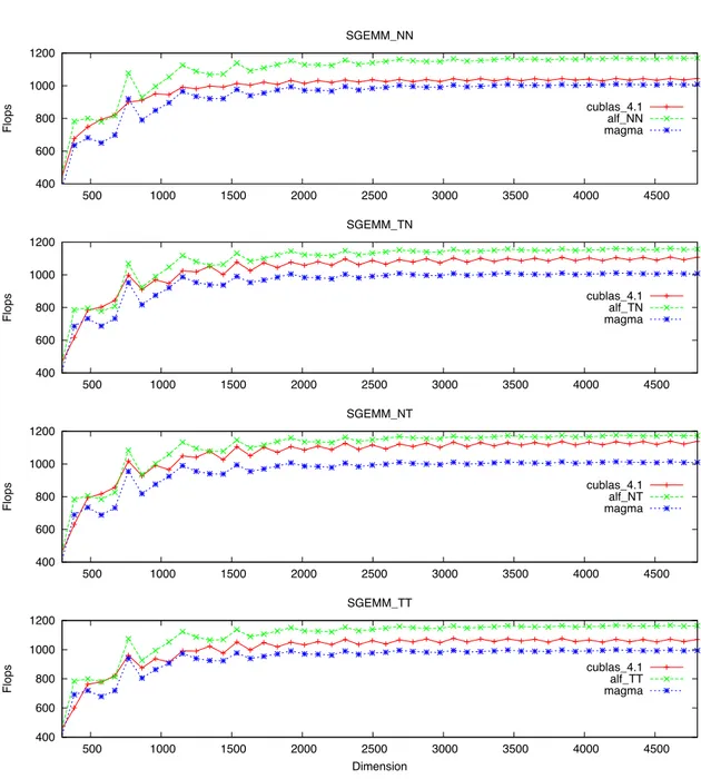
As in Figure 3, it is the performance comparison between our implementation (alf_sgemm), cublas from CUDA 4.1 and MAGMA library [5].
6
Conclusion
In this work, we analyzed the potential peak performance bound on Fermi GPU for SGEMM. We showed that the nature of Fermi instruction set and the limited issuing throughput of schedulers are the main limitation factors for approaching the theoretical peak performance. Guiding by the analysis, we further optimized the four SGEMM kernels. The 4 kernels achieved 11% (NN), 4.5% (TN), 3% (NT) and 9% (TT) better performance than cublas from CUDA 4.1. We also described how to use assembly code directly in a CUDA runtime source project and discussed the possible optimization methods for SGEMM on Kepler GPU and the possible peak performance that we can achieve.
References
[1] Asfermi. http://code.google.com/p/asfermi/.
[2] J. Kurzak, S. Tomov, and J. Dongarra. Autotuning gemm kernels for the fermi gpu. Parallel and Distributed Systems, IEEE Transactions on, PP(99):1, 2012.
[3] M. D. Lam, E. E. Rothberg, and M. E. Wolf. The cache performance and optimizations of blocked algorithms. SIGPLAN Not., 26(4):63–74, Apr. 1991.
[4] A. C. McKellar and E. G. Coffman, Jr. Organizing matrices and matrix operations for paged memory systems. Commun. ACM, 12(3):153–165, Mar. 1969.
[5] R. Nath, S. Tomov, and J. Dongarra. An improved magma gemm for fermi gpus, 2010. Inria
Bound the Peak Performance of SGEMM on GPU with software-controlled fast memory 11 400 600 800 1000 1200 500 1000 1500 2000 2500 3000 3500 4000 4500 Flops SGEMM_NN cublas_4.1 alf_NN magma 400 600 800 1000 1200 500 1000 1500 2000 2500 3000 3500 4000 4500 Flops SGEMM_TN cublas_4.1 alf_TN magma 400 600 800 1000 1200 500 1000 1500 2000 2500 3000 3500 4000 4500 Flops SGEMM_NT cublas_4.1 alf_NT magma 400 600 800 1000 1200 500 1000 1500 2000 2500 3000 3500 4000 4500 Flops Dimension SGEMM_TT cublas_4.1 alf_TT magma
Figure 3: SGEMM Performance
[6] G. Tan, L. Li, S. Triechle, E. Phillips, Y. Bao, and N. Sun. Fast implementation of dgemm on fermi gpu. In Proceedings of 2011 International Conference for High Performance Computing, Networking, Storage and Analysis, SC ’11, pages 35:1–35:11, New York, NY, USA, 2011. ACM.
RESEARCH CENTRE
RENNES – BRETAGNE ATLANTIQUE
Campus universitaire de Beaulieu 35042 Rennes Cedex
Publisher Inria
Domaine de Voluceau - Rocquencourt BP 105 - 78153 Le Chesnay Cedex inria.fr