HAL Id: hal-01082273
https://hal.archives-ouvertes.fr/hal-01082273v2
Submitted on 25 Nov 2014HAL is a multi-disciplinary open access archive for the deposit and dissemination of sci-entific research documents, whether they are pub-lished or not. The documents may come from teaching and research institutions in France or abroad, or from public or private research centers.
L’archive ouverte pluridisciplinaire HAL, est destinée au dépôt et à la diffusion de documents scientifiques de niveau recherche, publiés ou non, émanant des établissements d’enseignement et de recherche français ou étrangers, des laboratoires publics ou privés.
Improvement of efficient coupling and optical resonances
by using taper-waveguides coupled to cascade of UV210
polymer micro-resonators
Rigoberto Castro-Beltran, Nolwenn Huby, Goulc’Hen Loas, Hervé Lhermite,
David Pluchon, Bruno Bêche
To cite this version:
Rigoberto Castro-Beltran, Nolwenn Huby, Goulc’Hen Loas, Hervé Lhermite, David Pluchon, et al.. Improvement of efficient coupling and optical resonances by using taper-waveguides coupled to cas-cade of UV210 polymer micro-resonators. Journal of Micromechanics and Microengineering, IOP Publishing, 2014, 24, pp.125006. �10.1088/0960-1317/24/12/125006�. �hal-01082273v2�
Improvement of efficient coupling and optical resonances by
using taper-waveguides coupled to cascade of UV210 polymer
micro-resonators
R Castro-Beltran1, N Huby1, G Loas1, H Lhermite2, D Pluchon1 and B Bêche1,3
1 IPR UMR CNRS 6251, Université de Rennes 1, bât. 11B, 263 avenue Général Leclerc, 35042 Rennes, France. 2 IETR UMR CNRS 6164, Université de Rennes 1, bât. 11B, 263 avenue Général Leclerc CS 74205, 35042 Rennes Cedex, France.
3
IUF, Institut Universitaire de France, 103 bd St Michel, 75005 Paris, France. Email: bruno.beche@univ-rennes1.fr , nolwenn.huby@univ-rennes1.fr
Abstract
In this paper, we report the overall design, fabrication and optical characterization of single and multiple resonant micro-structures patterned on the UV210 polymer and shaped by adequate deep-UV lithography procedures. Various families of ring and racetrack forms are investigated with different geometrical dimensions linked to the micro-resonators and the specific taper-waveguides and gaps allowing the optimized coupling. Well defined photonic structures families in the sub-micrometer range obtained by this deep UV-light process are clearly confirmed through scanning electron microscopy. In order to evaluate and quantify the efficiency of the sub-micrometer coupling, the recirculation of the light and the quality of the optical resonance aspects, a global study including top view intensity imaging, spectral measurements and Fast Fourier Transform analysis is performed for all these devices based on single and multiple family resonators. The experimental TE-mode resonance
transmissions reveal a complete agreement with the period of the theoretically expected resonances. A maximum value of the quality factor Q = 3.5 x 10³ at 1035 nm with a 3.2 times higher resonance contrast is assessed for cascade of triple micro-resonators respect to the photonic devices based on only one micro-resonator. In addition, these UV210 circuits made of specific tapers coupling to cascade loops act directly on the improvement of the evanescent coupling and resonances in terms of quality factor and extinction rate, by selecting successively and more precisely the optical mode resonance. All these designs and low cost technological reproducible steps, and furthermore the devices and protocol measurements are markedly suitable for mass fabrication and metrology applications.
1. Introduction
Developing new photonic devices through simple, low cost and parallel fabrication steps has been over the last decade extremely important for biosensing and telecom applications [1-5]. In particular, the ability to fabricate systems with nanoscale features requires critical procedures that range from direct laser writing to photoresist-based patterning [6-10]. Because of the resolution limits on the patterning techniques, not all the lithography systems can generate photonic devices in the submicrometer scale. Two routes can be followed: the first one refers to a modification on the lithography systems by decreasing the exposure wavelength. Changing the presentation of the filters, as was done in the deep ultraviolet (DUV) lithography system, allows a reduction in the optical lithographic wavelength from 365 nm i-line to 248 nm [8]. The second route refers to the photonic circuit design strategies. Thus, in the case of microresonators, it consists in a vertical coupling between the bus waveguide and the resonant structure. Multilayer stack and submicrometer gap are then controlled by reactive ion etching process [11, 12].
To fabricate our photonic devices, we opted for DUV lithography using the chemically amplified (CA) UV210 photoresist as polymer [13]. This positive photoresist is now used for submicrometer photonic patterns [14, 15]. The evolution and capacity of this polymer to act as more classical photonic structures
have been demonstrated. Single-mode rib waveguides have shown off optical losses about few dB/cm whereas lateral coupling zones of few hundred nanometers have proven the possibility of developing first photonic structures [16, 17].
The capacity of emerging photoresist to be used for the development of photonic circuits, mainly constituted by resonant structure, demonstrated the capability for photonic miniaturization. Such resonators have proven to be useful on-chip integration for a large number of applications ranging from environment monitoring to wavelength filtering. For such applications, the shape of the resonances must present appropriate optical properties that are strongly connected to the fabrication process. Recently, serial of multiple micro-resonators on another material have found promising functionality as an optical element by providing more uniform resonance responses [18-21]. Cascade of multiple resonators, distributed with identical cavities, can enhance the optical transmission features without influence on the free spectral range (FSR). An improvement in the full width at half maximum (FWHM) through sharper roll-off resonances, results in an enhancement in the finesse and in the quality (Q) factor of the photonic devices [20, 22].
The aim of this paper is to investigate the capability of the UV210 polymer to support tapers coupled to different cascade of multiple Ring and RaceTrack micro-resonators by low cost and reproducible deep UV (DUV) lithography procedures. Section 2 reports all the global geometrical parameters of these family microstructures, describes the DUV lithography fabrication processes and the scanning electron microscopy (SEM) images highlighting the quality and reproducible aspects of such micro- and nano-scale integration systems. Moreover, the entire platform devoted to the measurements and the specific protocol is described. The overall optical characterization of the family structures using micro beam profile (MBP) system and optical spectral analyzer (OSA) coupled with fast Fourier transform (FFT) analysis are presented in Sections 3. The discussions presented in Section 4 emphasize the advantages of such integrated configurations on the improvement of optical resonances.
2. Design, fabrication and integration technologies of the tapers/micro-resonators structures
The details of two circuits shaped as tapers coupled to single micro-resonators under test are illustrated in figure 1.
Figure 1. Schematic representation and structural details of (a) single micro-Ring and (b) single micro-RaceTrack.
Parameters R, Lc and gap represent respectively the radius, the coupling length and the distance between the rib waveguides and the micro-resonators.
Figures 1(a) and 1(b) describe the geometrical parameters for the two different families defined as single Ring and single RaceTrack MRs respectively. As illustrated in figure 1, the resonators are coupled by two straight slowly tapered waveguides of 2µm width, assuring both single-mode optical propagation, an exaltation of the field in the taper and coupling zone, plus an efficient evanescent power-coupling into the MR [5]. The features and presentations on all the design of the devices under test, such as devices with one (Single), two (Double) and three (Triple) consecutive cavities, with Ring and RaceTrack shapes, with radius of R = 25 µm and R = 50 µm, allow us to classify them as presented in table 1. Since many different devices are tested, a nomenclature has been introduced for more simplicity: as an example SSR means Single Small Ring, DLRT means Double Large RaceTrack, whereas TSR means Triple Small Ring.
Table 1. Global classification and abbreviation of all the families of micro-resonators under test
Cavities Size Shape Nomenclature Single: S Small (S) Large (L) Ring (R) RaceTrack (RT) SSR, SLR SSRT, SLRT Double: D Small (S) Large (L) Ring (R) RaceTrack (RT) DSR, DLR DSRT, DLRT Triple: T Small (S) Large (L) Ring (R) RaceTrack (RT) TSR, TLR TSRT, TLRT
In addition, it is noteworthy that for devices with Double and Triple cavities, the micro-resonators keep their dimensions unchanged and the distance between two consecutive MRs has been chosen long enough in order to avoid direct interaction between two independent resonators.
2.1 Deep UV lithography processes on the micro- and nano- scale
The fabrication procedure of Single and cascade of Ring and RaceTrack MRs is schematically represented in figure 2. Devices are fabricated by DUV lithography and the whole process is performed in a class 100 cleanroom. The starting point of the micro-fabrication and engineering processes consists of a (1 0 0) silicon substrate covered with a 1.5 µm-thick thermal SiO2 layer acting as an optical lower cladding with n = 1.45 at 980 nm.
Figure 2. Scheme of global fabrication steps of a chip using DUV lithography procedures on quartz-mask. (a)
Transfer of waveguide patterns into the UV210 polymer. (b) Cross section representation of one of the Single devices after having developed and cured the sample.
A 1 µm-thick layer of the UV210 polymer is spin-coated on the SiO2/Si substrate. In order to evaporate the remaining solvent in the deposited layer, a softbake procedure is done before exposure. Single and cascade of multiple MRs patterns are transferred onto such UV210 polymer layer by using only one deep UV lithography exposure through quartz mask. Light exposure is performed using a UV lamp (HBO 1000 W/D, mercury short arc lamp from OSRAM) combined to a bandpass filter to obtain a 248nm insolation-wavelength. This is immediately followed by the post exposure bake (PEB) procedure which consists in putting the substrate on a hot plate to allow the UV210 polymer to complete the cross-linking. Before developing the serial of optical circuits on the chip, 10 minutes of cooling down allow the surface of the layer to capture oxygen which helps in the quality of the patterning of the devices. After this, the sample is immersed in the developer solution to remove insolated zones and reveal the micro and sub-micrometer patterns as the gap or coupling zones tapers/MRs. Finally, the last step consists in fully cross-linking the polymer layer by curing process also referring as hard bake step. This process is realized in an oven with temperatures ranging from 100 °C-150 °C during 24 hours.
2.2 Scanning electron microscopy and quality of circuits
Scattering losses from interfaces imperfections associated with fabrication procedures are fundamental aspects for efficient miniaturization of photonic circuits [19, 23]. It is particularly important to follow the structural qualities like shape and surface conditions of the photonic devices before all the specific optical characterizations. SEM images have been taken systematically on each device and some of the results are gathered on figure 3.
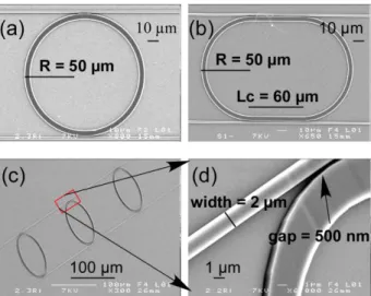
Figure 3(a) and figure 3(b) present respectively the top-view perspectives of the SLR and SLRT. Both photonic devices are well defined presenting a radius of R = 50 µm, a width of W = 5 µm and for SLRT a coupling length Lc = 60 µm. Figure 3(c) shows the tilted top-view of the TLR device confirming constancy on the properties of the cascade of the three Ring microresonators. Figure 3(d) presents the most important aspect on this kind of configuration: coupling zone and quality of manufacture on the sidewalls of the photonic devices. The measurement of the gap width by SEM image treatment leads to mean value of 531 nm for the ring and 500 nm for the racetrack. The standard deviation calculated for several measurements along the coupling length for these structures are 14 nm and 23 nm respectively, showing the high accuracy of the DUV lithography method.
Figure 3. Visualization of the structural details through SEM images of the devices: (a) SLR, (b) SLRT, (c) tilted
views of TLR and (d) a zoom on the coupling zone of the Ring micro-resonators forming the device.
3. Experimental protocol, optical injection and coupling
The experimental platform is presented in the schematic diagram of figure 4. Two optical broadband sources are used to characterize the photonic circuits patterned as tapers/MRs. The first one is centered at 845 nm with a FWHM of 30 nm of and the second one at 1025 nm with a FWHM of 45 nm.
Figure 4. Experimental setup. Two broadband sources are used to characterize the different microresonators. XYZ
nanometer displacement mounts are used to control the alignment of the incident NIR objectives (x20) and of the device position. An optimized control of the light injection, propagation and detection is achieved through IR camera, optical powermeter and MBP system. Microresonators resonances are finally analyzed with an Optical Spectrum analyzer. SMF: Single mode fiber.
The outputs of both sources are connected to single mode fibers and coupled to a x20 objective to collimate the optical beams. The transverse electric TE polarization is controlled with a polarizer. The beam is then focused and coupled to the devices under test through one of the inputs of the rib waveguides with a x20 objective. The device and the objective for light injection are positioned on piezo electric nano-positioners. The beam at the output of the device is collected and collimated by a x20 objective and simultaneously monitored with a IR camera and an optical powermeter. Once the maximum
of power is obtained, the optical powermeter is replaced by an optical spectra analyzer (OSA Ando AQ-6315E) for resonances detection analysis.
A Micro Beam Profiler (Newport-MBP) is used to corroborate the light propagation along the rib waveguides and the loop of the resonant structures. It is positioned on top of the devices with the aim of collecting their scattered light. Figure 5 presents the recorded image for TLR device. Figure 5(a) highlights the light propagation along the three loops of the Ring micro-resonators. It also displays the coupling light along the add port through the three coupling regions belonging to each micro cavity thus confirming the evanescent coupling between rib waveguides and serial of MRs.
The corresponding cross-sectional intensity measurements are presented on figure 5(b). This intensity profile allows an estimation of the geometrical dimensions such as the diameter of the Rings (100 µm) and the width between the two sidewalls that form the cavity (5 µm). These measurements reproduce well the dimensions obtained by SEM which demonstrates the accuracy of this method to estimate geometrical conditions of one photonic structure.
Figure 5. Field intensity pattern of the TLR. (a) Confirmation of the light propagation through the rib waveguides
and recirculation into the loops. (b) Intensity profiles of the cross-sectional line visible on the figure 5(a).
4. Optical characterizations and resonances, spectral analysis, results and discussions
Referring to the experimental setup of figure 4, we characterized all the families and series of micro-resonators by using two different large bandwidth sources. After having optimized the intensity of the light emerging from the waveguide, this signal is coupled to the OSA to observe the multiple resonances corresponding to each kind of MR. A complementary optical characterization over one tapered waveguide under the same geometrical conditions allowed us to confirm that the modal propagation properties remain free of conversion and of internal interferences, which means a completely adiabatic process into the tapered waveguide and between the micro-resonators [5].
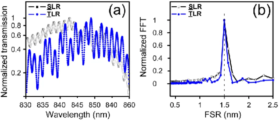
As an example, figure 6 shows the comparison between the normalized intensities at the transmitted ports of the SLR and TLR devices by using the broadband source centered at 845 nm. Deeper resonances are clearly observed for cascaded MRs compared to single MR. Indeed, 2.5 times higher contrast is calculated for those resonances obtained for the TLR device in comparison with its corresponding registered for the SLR device. We can also notice on figure 6(a) a slight wavelength shift between their corresponding
resonances transmissions. This is not surprising since both devices are from two independent photonic chips and are optically characterized under different OSA alignment and thermal conditions.
Figure 6. (a) Resonances transmissions spectra for SLR and cascade of TLR. (b) Corresponding normalized fast
Fourier transform (FFT) for both devices.
The most important optical parameters that describe the response and behavior of a microresonator are the free spectral range (FSR), the FWHM, the quality factor Q and the finesse F [17]. All these features hinge on the losses and the coupling coefficients describing each MR. Regarding resonance of the cascade of TLR in figure 6, taking into account the geometrical conditions and the refractive index nUV210 of 1.553 at 850 nm, FSR-values ranging from 1.41 nm to 1.52 nm are theoretically expected between λ = 830 nm and λ = 860 nm wavelengths respectively. Possible slight difference between the theoretically and experimentally obtained FSR-values can be explained by considering the effective group index (ng) which is inherent to any optical large bandwidth source.
The normalized FFT responses, presented in figure 6(b), reveal the good agreement of the theoretical FSR-value with the experimental one. Through Lorentzian fitting, values of 0.6 nm of FWHM at λ = 848.21 nm, Q-factor of 1.4×10³ and F of 2.6 are calculated. Those values are improved compared to SLR showing calculated values of 0.9 nm of FWHM at λ = 848.03 nm, Q-factor of 0.95×10³ and F of 1.6. We chose to not present in figure 6 the resonance spectrum of the DLR device for more clarity, it is nevertheless clear that cascaded micro-resonators improve greatly the photonic circuit properties. DLR device presents values of 2 times higher contrast in the depth of the resonances, in comparison with the SLR device.
Figure 7. (a) Experimental normalized responses of the SSRT and TSRT and (b) their corresponding normalized
Moreover, we characterized in parallel all the serial of MRs by using a large bandwidth source centered at 1025 nm. As an example, figure 7 shows the resonance spectra of the SSRT and of the TSRT devices. As previously demonstrated, for the SLR and TLR resonance transmissions, the multiple loops corresponding to multiple RaceTrack MRs also improve the optical properties since the resonance peaks are deeper and with higher extinction ratio. For this case, 3.2 times of higher contrast is calculated for the resonances registered for the TSRT device in comparison with those obtained for the SSRT device. The resonance spectrum of the DSRT device (not shown here) presents values of 1.4 times higher contrast in comparison with the SSRT device.
Under these geometrical and experimental conditions, we expect theoretical FSR-values ranging from 2.3 nm to 2.7 nm between λ = 1000 nm and λ = 1060 nm wavelengths respectively. The FFT analysis, presented in the figure 7, highlights a main contribution at 2.9 nm for TSRT unlike SSRT that present a wider range in the period of the resonances which are disseminated around 2.8 nm. This is due to the cascade of multiple loops, which besides improving the properties of the resonance frequencies, can act as modal filters by selecting successively and then more precisely the optical mode resonance. When multiple frequencies are traveling along the resonator, this works as a very dispersive photonic structure and slight deficiencies on the quality of fabrication enhance the delaying process. Nevertheless, cascade of resonators restrict this delayed condition by limit the bandwidth of the frequencies that can be delayed. Here, resonators in multistage configuration act as high order optical filters based on the same principle used in electronics [22]. Possible slight difference between the theoretically and experimentally obtained FSR-values can be explained by considering the dispersion of the effective group index (ng) inherent to the use of optical large bandwidth source.
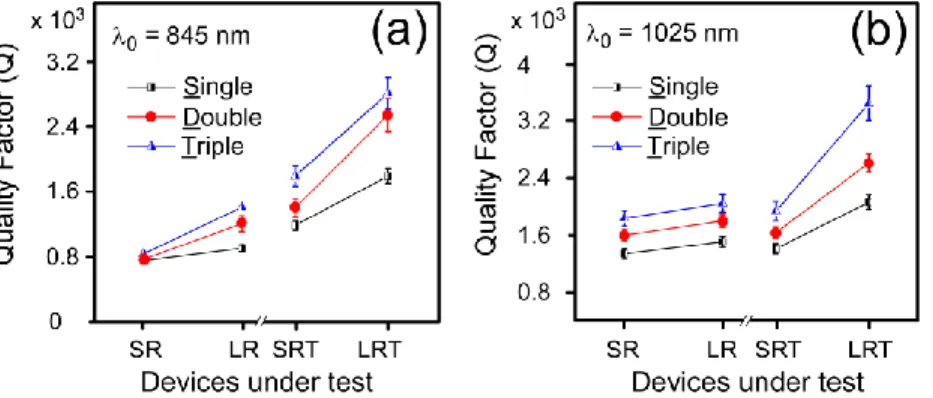
In order to analyze further the role of geometry and number of devices as well as light source on the resonators behavior, figure 8 summarizes the obtained results on the evolutions of the Q-values for the series of micro-resonators under test.
Figure 8. Evolution of the Q-factor values as a function of the multi-stage configuration: single (line-square),
double (line-circle) and triple (line-triangle). Q-values obtained by using the broadband source (a) centered at 845 nm and (b) centered at 1025 nm.
The graphs present an evolution of their Q-values according to several parameters of all family-devices such as the shape, the dimension, the number of resonant structures and the wavelength excitation sources. A clear enhancement is observed on the Q-factor magnitudes as the number of loops in the photonic devices increases. Moreover, the two groups of devices (Ring and RaceTrack) present also a positive evolution on their Q-values when MRs with longer geometrical dimensions are analyzed. This is mainly because the Q-factor presents a linear dependence with the length of the MR.
The Q-values obtained through these configurations represent an enhancement respect to our previous publication on which maximum Q-values of 850 for disks and of 630 for stadium were obtained at 850
nm of excitation wavelength [17]. These results were obtained for filled structures and have to be compared with their corresponding empty structure investigated here, e.g., single Ring and single RaceTrack. Through empty resonant structures, an improvement in the resonance transmission properties and Q-factor is expected since these are known to better confine the light and to promote the single mode operation. Nevertheless, the enhancement on the Q-values is temperate, less than one order of magnitude, which can be explained in terms of roughness. Indeed, the losses are mainly dominated by the sidewalls roughness that is doubled in empty structures. In addition, a longer extension of the coupling zone can contribute to both a strong coupling strength and with added light scattering too [19, 23].
Another interesting aspect appearing on figure 8 is related to the selection of the wavelength excitation source. We can note that, all the photonic devices enhanced their responses under the broadband source center at 1025 nm which is in good agreement with Ref. [23]. Apparently, the coupling strength, mainly due to elongating the gap zone and, the losses, basically dominated by the two sidewalls of the photonic devices, present a different behavior when the two broadband sources were used. This behavior can be explained as following: backward reflections due to sidewall roughness in the photonic devices limit their resonance properties. At shorter excitation wavelength the scattering of the propagating light is stronger which can cause back-scattering into a counter-propagating mode which makes that the Q-value decreases.
Finally the evolution presented in figure 8 demonstrates an enhancement on the Q-values as the number of loops involved in the photonic circuit increases. No saturation effect in the Q-values suggests that improvement on the optical response is still feasible and will be subject of further study. Indeed, different routes may be tested. On the one hand post-deposition treatment (thermal or plasma) can improve the roughness of the side walls and optical losses directly connected to the Q factor. On the other hand, a different approach will be to pattern the submicronic gap by e-beam lithography.
4. Conclusion
The high capacity of the chemically amplified UV210 polymer to support cascade of various families of micro-resonators (MRs) with different geometries and dimensions is presented in this work. The adequate quality of the fabrication process by deep UV lithography is validated by SEM images and confirmed by micro beam profiles (MBP) imaging. In particular, the sub-micrometer gap remains constant along the coupling zones for cascade of multiple MRs showing a gap along the coupling zone of 531 +/- 14 nm and 500+/-23nm for ring and racetrack respectively. In addition, MBP demonstrates the efficient evanescence coupling between the taper-waveguides and the resonant cavities of the devices due to the adequate exaltation of the optical field. Through spectral analyses and protocol measurements, we verified the excellent agreement of the theoretical and experimental FSR-values of all the series of families of MRs under test. A systematical study on single and cascade of Ring and RaceTrack MRs is presented in order to correlate geometrical aspects and cavity efficiencies. The improvement on the resonance properties is due to the structural organization of the multiple loops presented in cascade of MRs. Cascade of three RaceTrack microresonators show the best optical response, presented values of Q = 3.5 × 10³ and 3.2 times higher resonance contrast respect its corresponding single devices. In addition, the FFT-anlyses of the optical responses of cascade of multiple cavities demonstrate to have a very high capacity to discriminate between modal propagation that does not correspond to the opto-geometrical conditions of the resonator. The ability of new organics, as the CA UV210 polymer, to undergo integrated optics transformations that contribute to the trend of photonic circuit miniaturization is demonstrated through the design of various associations tapers/MRs which are suitable for different purposes like filters or thermal sensors.
This work was supported by Région Bretagne (SAD program).The authors are grateful to the assistance of F. Gouttefangeas and L. Joanny from the CMEBA in University Rennes 1 for SEM work.
References
[1] De Vos K, Bartolozzi I, Schacht E, Bienstman P and Baets R 2007 Opt. Exp. 15 7610.
[2] Grossmann T, Wienhold T, Bog U, Beck T, Friedmann C, Kalt H and Mappes T 2013 Light Sci.
Appl. 2 e82.
[3] Bêche B, Pelletier N, Gaviot E, Hierle R, Goullet A, Landesman J P and Zyss J 2005 Microelectron.
J. 37 421.
[4] Flueckiger J, Grist S M, Bisra G, Chrostowski L and Cheung K C 2011 in Proc. of SPIE 7929 79290I.
[5] Beck T, Schloer S, Grossmann T, Mappes T and Kalt H 2012 Opt. Exp. 20 22012.
[6] Liu Z-P, Li Y, Xiao Y-F, Li B-B, Jiang X-F, Qin Y, Feng X-B, Yang H and Gong Q 2010 Appl.
Phys. Lett. 97 211105-1.
[7] Sheng Z, Liu L, He S, Van Thourhout D and Baets R 2009 GFP '09. 6th IEEE Int. Conf. 122. [8] Sahoo P B, Vyas R, Wadhwa M and Verma S 2002 Bull. Mater. Sci. 25 553.
[9] Grossmann T, Schleede S, Hauser M, Beck T, Thiel M, Freymann G v, Mappes T and Kalt H 2011
Opt. Exp. 19 11451.
[10] Grossman T, Hauser M, Beck T, Gohn K C, Karl M, Kalt H, Vannahme C and Mappes T 2010
Appl. Phys. Lett. 96 013303-1.
[11] Luan L, Cho S-Y and Jokerts N M 2007 in Proc. of ECTC '07 2035.
[12] Delezoide C, Salsac M, Lautru J, Leh H, Nogues C, Zyss J, Buckle M, Ledoux R I and Thanh N C, 2012 IEEE Photon. Tech. Lett. 24 1041.
[13] http://hone.mech.columbia.edu/wiki/lib/exe/fetch.php?media=wiki:uv210.pdf
[14] Teo S H G, Liu A Q, Singh J and Yu M B, 2004 J. Vac. Sci. Technol. B 22 2640.
[15] Jagar S, Singh N, Mehta S S, Agrawal N, Samudra G and Balasubramanian N 2004 Thin solid
Films 462 1.
[16] Duval D, Lhermite H, Godet C, Huby N and Bêche B 2010 J. Opt.12 055501.
[17] Pluchon D, Huby N, Lhermite H, Duval D and Bêche B 2012 J. Micromech. Microeng. 22 085016.
[18] Tobing L Y M A L and Chin M-K 2014 Proc. of SPIE 6996 69961G-1. [19] Chao C-Y 2005 Ph. D. dissertation, Elec. E, UM, Michigan, US-MI.
[20] Timotijevic B D, Gardes F Y, Headley W R, Reed G T, Paniccia M J, Cohen O, Hak D and Masanovic G Z 2006 J. Opt. A: Pure Appl. Opt. 8 S473.
[21] Salleh M H M 2011 Ph. D. dissertation, Elec. E, GIC. [22] Dumeige Y 2009 IEEE Photon. Technol. Lett. 21 435.