HAL Id: hal-02181455
https://hal-univ-rennes1.archives-ouvertes.fr/hal-02181455
Submitted on 25 Nov 2019
HAL is a multi-disciplinary open access
archive for the deposit and dissemination of
sci-entific research documents, whether they are
pub-lished or not. The documents may come from
teaching and research institutions in France or
abroad, or from public or private research centers.
L’archive ouverte pluridisciplinaire HAL, est
destinée au dépôt et à la diffusion de documents
scientifiques de niveau recherche, publiés ou non,
émanant des établissements d’enseignement et de
recherche français ou étrangers, des laboratoires
publics ou privés.
Mandatory matching between microelectronics industry
and higher education in engineering toward a digital
society
O. Bonnaud
To cite this version:
O. Bonnaud. Mandatory matching between microelectronics industry and higher education in
engi-neering toward a digital society. Uskov V.; Howlett R.; Jain L. (eds). Smart Education and e-Learning
2019, 144, Springer Science and Business Media Deutschland GmbH, pp.255-266, 2019, Smart
Inno-vation, Systems and Technologies, �10.1007/978-981-13-8260-4_24�. �hal-02181455�
Mandatory Matching Between Microelectronics Industry
and Higher Education in Engineering Towards a Digital
Society
Olivier Bonnaud1,2
1
GIP-CNFM, Minatec, Grenoble, 38016, France
2
Sensor and Microelectronics Department, IETR, University of Rennes 1, France [email protected]
Abstract. The evolution of the world towards the digital society requires the
development of many connected objects, the basis of the Internet of Things (IoT), with a very wide spectrum of applications. These connected objects are based on communication protocols, embedded software but more fundamentally on the hardware that corresponds to the physical realization of the objects. Mi-croelectronic technologies are therefore at the heart of all these devices and sys-tems. This exponential evolution, is the result of more than fifty years of in-creasing integration, which is becoming very complex and combining many technological approaches and multidisciplinary architectures. The future indus-try 4.0 requires skills and competencies in microelectronic design and techno-logical fabrication. At the same time, investments in manufacturing plants and design software follow the same exponential cost trend. To meet the needs of the industry, training must be constantly updated with good know-how on dedi-cated tools and equipment. To achieve this objective, higher education must be organized to provide students with knowledge and skills. A dedicated organiza-tion must be set up with common platforms that allow technological equipment and Computer-Aided-design tools (CAD) to be shared. This paper deals with the French national network which has proven its effectiveness in higher educa-tion in microelectronic engineering for more than thirty years. After a presenta-tion of its organizapresenta-tion and objectives, several examples of innovative practical work covering the different fields of application are given.
Keywords: Microelectronics, Higher Education structuring, Industry 4.0.,
En-gineering.
1
Introduction
Everybody knows that the XXI century will be the era of the fourth industrial revolu-tion with the progressive introducrevolu-tion of digital society, with connected objects, smart objects, and new manufacturing governed by robotics, internet of things and artificial intelligence. They are all included in the Internet of Things (IoT). The production should be performed by the so-called industry 4.0. This means the development of
computer sciences associated to new objects and systems that can fulfil the adequate missions thanks to new technologies.
The core of these objects and tools capable of integrating software is microelec-tronics. In practice, the real evolution towards this new world has been possible thanks to the fabulous evolution of microelectronic technologies, based on the inte-gration of billions of transistors per circuit. This evolution has made it possible to store billions of data, to process these data with more than one hundred billion opera-tions per second but also to communicate them with such a flow. In addition, microe-lectronics technological processes are capable of developing sensors and actuators that are the links between the real and physical world and digital space. Behind this physical evolution, huge teams of engineers, technicians and researchers have been working since the early 1960s. The new industry 4.0 plants, requires skills and com-petencies not only in robotics and production management, but also in microelectron-ic design and technologmicroelectron-ical manufacturing. The challenge is to meet the needs of the industry. Practical training must be constantly updated with good knowledge of dedi-cated tools and equipment. To achieve this objective, higher education must provide students with knowledge and skills on increasingly expensive tools. A dedicated and strongly industry-related organization must be set up with common platforms allow-ing the sharallow-ing of technological equipment and CAD tools. This article deals with the French national microelectronics network (CNFM [1-2]) that has proven its worth in higher education in microelectronics engineering for more than thirty years. After a presentation of the context, the organization and objectives are highlighted and sever-al examples of innovative practicsever-al work are given.
2
Trends of the microelectronics industry
2.1 Evolution of the integration in microelectronics
The world evolution towards a digital society is highly dependent on microelectronic technologies, which are therefore at the heart of all devices and systems involved in IoT. This evolution, exponential in practice, is the result of more than fifty years of increasing integration, which is becoming very complex and combines many techno-logical approaches and multidisciplinary architectures. Figure 1 shows the evolution of integration into a chip predicted by G. Moore and called Moore's Law [3] and the recent evolution of systems that include systems on a chip or in a package that grow exponentially in a similar way to Moore's Law [4] and thus allow connected objects to be created.
2.2 Towards a digital society: connected objects
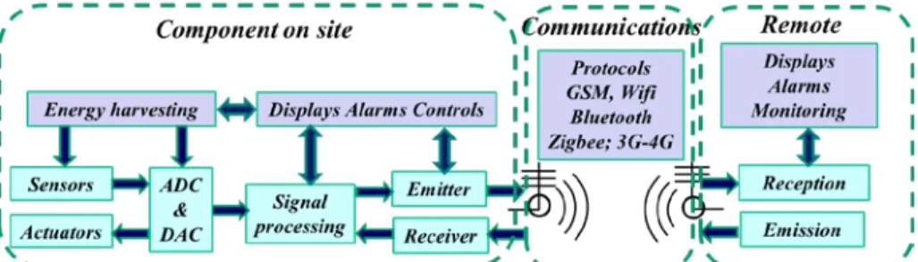
As we have already presented [5], connected objects make it possible to analyze and control many aspects of society's needs remotely. They are first of all composed of on-site functions such as sensors, actuators, and signal processing as shown Figure 1, and at remote sites, of a transmitter and receiver, a signal processing system and a remote control system.
3
Fig. 1. Evolution of the integration during the last sixty years. The density of transistors per die
increased exponentially following the prediction of G. Moore [3]. Since 1995, the integration had started a new exponential evolution [4], the density of transistors reaching 1013.
Fig. 2 Simplified architecture of a connected object with on-site component and remote
com-ponent (after O. Bonnaud et al. [5]). It is mainly composed of sensors, actuators, signal con-verters, processor, emitter-receiver, visualization, alarms and controls, and energy harvesting.
2.3 Multidisciplinarity of the fields of applications
The most important interest of connected objects is related to the wide spectrum of their applications. All the major areas of modern society are concerned. These include communications and information, health, safety, environment, energy, transport, agri-culture, manufacturing in industry 4.0. As a result, future designers of these objects must have skills and abilities in the field of microelectronics, but also be able to work in teams with specialists in the fields of application [6].
2.4 Heterogeneous integration toward systems on chip and systems in package
The connected objects must integrate new functions adapted to the application fields. These functions can have physical, chemical, and biological-based detectors and actu-ators combining a large variety of architectures and physical elements (optical, me-chanical) thermal dependence devices, chemical or biological functionalization. In many cases, they need also an energy autonomy; this means integration of batteries or electrical charge storage, and energy harvesting cells. This is becoming possible thanks to a heterogeneous integration (figure 3) [7]. It is clear that the third dimension
(3D) takes more and more importance at the level of ULSI (Ultra large Scale Integra-tion) for example with CoolcubTM [8]) or in packaging that combines several technol-ogies as thin film technoltechnol-ogies or Micro-Electro-Mechanical systems (MEMS).
Fig. 3. Diversity of the heterogeneous integration (After B. Bottoms [9]). Many functions are
integrated involving several technologies and 3D stacking.
In summary, new device and packaging architectures are needed to meet future market demand and to develop connected objects for industry 4.0. The consequence is that in 2018 the world's microelectronics activities represented an income of more than 480 billion US dollars, while the global activities involving microelectronic de-vices represented more than 6.8 billion US dollars as shown in Figure 4 [10]. The challenge is today to have competences and skills adapted to the development of fu-ture technologies and to the fufu-ture market. An effort must be made in the Higher Edu-cation and more especially in microelectronic engineering.
Fig. 4. Relative importance of microelectronics activities for developing future objects in the
global activities. The amplifying ration is close to 16 (After G. Matheron [10], with updating in 2017).
3
Higher education meeting the industry needs
3.1 Evolution of the knowledge acquisition in the digital environment
With the development of computer equipment, combined with the increase in storage capacity, communications and Internet, many new tools dedicated to online higher education have been created. One can mention the massive open online courses
5
(MOOC's) and the whole family of these online tools [11]. Several tools have been developed in the field of microelectronics [12] and have been discussed within the microelectronics community about the opportunity and threat of the global dissemina-tion of these tools. Indeed, if MOOCs are good theoretical learning tools and can change the way-people learn [13], they have a low effectiveness for the acquisition of know-how, which is an essential skill for engineers [14].
3.2 The know-how: a mandatory complement of the knowledge
Indeed, the use of MOOCs has some limitations in engineering sciences. In the field of micro and nanoelectronics, the online presentation of the electrical behavior of an integrated circuit remains essentially virtual. Due to their complexity, it is almost impossible to take into account all the physical and environmental parameters that can affect their electrical behavior. The simulation models are always approximate. A characterization of the actual (and physical) product is required to warranty the final properties of the circuits. Thus, practice is the key to understanding and acquiring skills [15]. It is fundamental for innovation [16], and producing innovative objects.
3.3 Needs of mutualization of the microelectronics engineering training
As mentioned above, the field of microelectronics and nanotechnology is undergoing a huge evolution towards complexity, heterogeneity of technologies and multidisci-plinarity. The corresponding practice requires very expensive tools and equipment, both in CAD using dedicated software and in cleanroom manufacturing processes, or in physical characterization and electrical testing. The only appropriate solution is to organize a network with several platforms common to several academic institutions in the same area and to share expenses between users. This approach is realistic in the context of a national network that can obtain several financial supports from public agencies, the Ministry of Higher Education and industrial partners.
4
The French National network for microelectronics education
4.1 Constitution of the CNFM network: academic/industry partnership
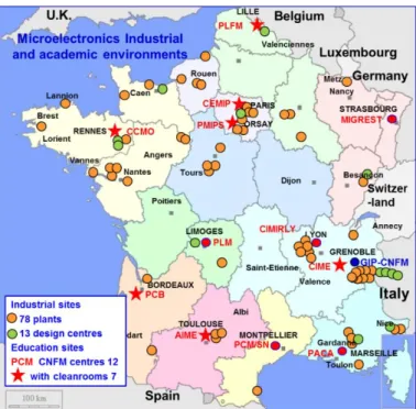
The microelectronic higher education in France is organized through a 35-year old national network, the National Coordination for Education in Microelectronics and Nanotechnologies, recognized by the Higher Education Ministry [1]. This network is composed of twelve academic members that have in charge the twelve common cen-ters spread over the French territory as shown figure 5. It also includes two represen-tations of industrial organizations and especially the most representative association ACSIEL Alliance Electronics consortium [17]. The industrial partners consider the training activities as an important factor for maintaining and developing electronics in France, and thus provide the network with valuable advice necessary.
Fig. 5. French academic and industrial activities in microelectronics. The 12 CNFM common
centers (red labels) manage platforms for practice training.
4.2 The missions and the strategy of the CNFM network
The very essence of the GIP-CNFM network is to share platforms because of their very high equipment and operating costs, but also to share pedagogical approaches and good practices towards students trained in initial training or LifeLong Learning (LLL). Collaboration within the network exists in several forms, through the sharing and common use of technological and design platforms, and through collaborative work in the context of national, or international, multi-year projects and through ped-agogical days and brainstorming seminars. These joint activities allow for the ex-change of knowledge and practices in order to produce and disseminate knowledge and know-how to the entire academic community.
4.3 The main results of the network
The 12 centers offering many training platforms receive yearly more than 90 degrees in its 7 clean rooms and 81 platforms covering most aspects of electronics, i.e. basic silicon microelectronic technology and design, low-power electronics, power elec-tronics, embedded elecelec-tronics, RF and millimeter wave elecelec-tronics, MEMS, biologi-cal MEMS (BioMEMS), organic electronics, thin-film technologies, photovoltaic technology. More than 16,000 students are users of the platforms each year, represent-ing more than 890,000 hours-students per year of trainrepresent-ing.
7
4.4 Strategy of the CNFM network towards know-how and innovation
In order to meet societal needs directly related to technological change, the content of practical training must be constantly updated. To this end, the management has a poli-cy oriented towards an innovative approach, both in the content of practical training and in pedagogical approaches. In 2011, the network applied for an innovative na-tional program under the Excellence in Higher Education Initiative. The FINMINA project (Innovative Formation in Microelectronics and Nanotechnologies) of the CNFM network has been accepted [18]. This is an eight-year project dedicated to innovation. This associated financial support enables the twelve joint centers to de-velop innovative practices mainly oriented towards new technologies for IoT.
5
Innovative practice
5.1 Know-how at the heart of the microelectronics field: innovative platforms
The innovative practice is first of all dedicated to the field of microelectronics and nanotechnologies. Indeed, this field is directly connected to the Moore’s Law and More than More’s evolution. New software for modeling the elementary devices for which the dimension reaches the nanoscale, new tools for CAD able to design very complex analog and digital circuits that contain billions of transistors, but also very high frequency modules for the transmission a very high flow of digital data, must be introduced in the content of the CAD platforms of the network. In addition, the heter-ogeneous technology assembling that combines many functions involved in connected objects must be designed with new multi-physic simulators in order to include in the systems sensors and actuators, significant components of the connected objects. All the students at the level of master of engineering must have some know-how of these tools that are used in the research centers and in the companies. Because the perfor-mances are directly linked to the fabrication process, the innovative platforms are created in order to prepare the students to the novel technologies such as, 3D elemen-tary devices, optoelectronics involving III-V compound materials, thin film technolo-gies, large area electronics for displays and energy conversion, flexible electronics, and more recently “plastronics”, for the most known ones. Specific training on tech-nological platforms are thus created and introduced in the menu of the users.
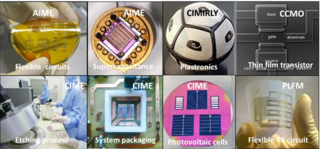
5.2 Concrete examples of innovative practice realized in the centers
With more than 80 new platforms set up in the twelve microelectronic centers of the network since 2012, several training activities are described below. Figure 6 shows a selection of achievements designed, manufactured and tested by students as part of their initial training or of advanced training. These are mainly master of engineering students but also PhD students in further training, or employees of companies in LLL. For each achievement, the microelectronics center is mentioned in the figure.
The diversity of the topics is shown: from integrated devices in bulk silicon tech-nology to silicon thin film transistors for displays, sensors or actuators [19], flexible
electronics or radiofrequency circuits, and three dimension electronic on plastic (called “plastronics”, for example [20]). Many other examples are available on the website of GIP-CNFM [1]. The topics are mainly involved in the development of the connected objects and meet the industry needs.
Fig. 6. Selection of achievements made by the students on the training platforms. The type of
training and the name of the center are mentioned in each picture. The diversity of topics is great. Many other examples are available on the CNFM network's website [1].
5.3 Contribution of the network to the education of graduate students
The strategy of innovation is adopted by all the members of the network [21]. Since 2012, each year, new practice that can be suggested by the industry representatives are set-up and proposed to the user formations. The managers of these formations progressively introduce the new practice in their menus. Figure 7 shows the signifi-cant growth of the innovative practice during the seven past years.
Fig. 7. Evolution from 2011 to 2018 of the number of users in the twelve common centers of
the CNFM network on innovative practice platforms. It is clear that the initial training is much more concerned.
9
The growth slope is close to 1,000/year. One can notice that the most significant component of this growth is generated by other disciplines that are more and more attracted by the multidisciplinary approach of the microelectronics field. For example, mechanicians are concerned by the MEMS, whereas biologists and medical specialists by the BioMEMS.
6
Conclusion
The societal evolution is definitely oriented towards the digital world with connected objects and IoT that can respond to many societal challenges such as health, environ-ment, security, transport or energy. The training of students must meet the needs of the company by providing knowledge and know-how adapted to these future chal-lenges. Because microelectronics is at the heart of all new objects, it is very im-portant, on the one hand, to prepare these specialists for the specificities of this field, and on the other hand, to raise awareness among a wider community of students from other disciplines in order to be better prepared to team working in the multidiscipli-nary approach to potential applications.
Moreover, the tools used in the field of microelectronics and its applications are becoming so complex and expensive that the most realistic solution for training in know-how, which is compulsory, is to pool infrastructure, software, and operating resources. This approach adopted by the French microelectronics network makes it possible, on the one hand, to minimize the cost and, on the other hand, to train future graduates on efficient, recent and, if possible, implemented tools in companies. This guarantees a good adaptation of training to the labor market, a good matching be-tween training structures and companies, and thus ensures a professional future for graduates.
7
Acknowledgment
The author wants to thank all the members of the French GIP-CNFM network for they contribution to this work, which is financially supported by French Education Ministry and by IDEFI-FINMINA program. A special thanks to L. Chagoya-Garzon, secretary of GIP-CNFM for her fruitful advice for the redaction of this paper.
References
1. CNFM: “Coordination Nationale pour la formation en Microélectronique and nanotech-nologies” (National Coordination for Education in Microelectronics and Nanotechnolo-gies). website: www.cnfm.fr; last access January 2019.
2. O. Bonnaud, P. Gentil, et al., GIP-CNFM: a French education network moving from mi-croelectronics to nanotechnologies. Proc. of EDUCON’11; 3-6 April 2011, pp 122-127, ISBN978-1-61284-641-5, Amman (Jordan) (2011).
3. G.E. Moore, “Cramming more components onto integrated circuits”, Electronics Maga-zine, 38 (8), 114-117 (1965).
4. T. Simonite, “Moore’s Law Is Dead. Now What?”, MIT Technology Review, https://www. technologyreview.com/s/601441/moores-law-is-dead-now-what/ May 13 (2016).
5. O. Bonnaud and L. Fesquet, Innovation for education on Internet of things, International Conference on Advanced Technology Innovation (ICATI’2018), Proc. of Engineering and Technology Innovation, PETI, vol. 9, pp. 01-08, Krabi (Thailand) (2018).
6. O. Bonnaud and L. Fesquet, “Towards multidisciplinarity for microelectronics education: a strategy of the French national network”, Proc. of IEEE Microelectronics System Educa-tion Conference (MSE), Publisher: IEEE, 4 pages, Pittsburg (MS), USA, (2015).
7. B. Bottoms, System Level Design and Simulation for Heterogeneous Integration Electron-ic Design Process Symposium, SEMI, Milpitas, Sept. 21‐22, California (USA) (2017). 8. P. Batude, et al., Demonstration of low temperature 3D sequential FDSOI integration
down to 50nm gate length, Symposium on VLSI Technology Digest of Technical Papers, pp. 158-159 (2011).
9. O. Bonnaud, Know-how needs for higher education in nanoelectronics: French CNFM network strategy, ICnano201810-12 October 2018, Advanced Materials Proceedings, vol. 3, 8 pages, Stockholm (Sweden) (2018).
10. G. Matheron, Microelectronics evolution, Keynote, European, Microelectronics Summit, Paris (France), Nov. (2014).
11. A. Fox, “From MOOCs to SPOCs”, in Proc. of ACM, Vol. 56 No. 12, pp. 38-40 (2013) 12. L. Stuchlikova, A. Kosa, P. Benko, D. Donoval, “Massive open online courses in
microe-lectronics education”, Proc. of 10th EWME 2014, 14th-16th May, pp. 31-36 Tallinn (Esto-nia, (2014).
13. J. Littlefield, What Makes a Good Online Course? http://distancelearn.about.com/od/isitfor you/a/How-Moocs-Are-Changing-The-Way-People-Learn.htm, last access January 2019 14. O. Bonnaud, New Vision in Microelectronics Education: Smart e-Learning and
Know-how, a Complementary Approach. © Springer International Publishing AG, Springer Na-ture 2019 V. Uskov et al. (Eds.): KES-SEEL-18 2018, SIST 99, pp. 267–275 (2019). 15. O. Bonnaud and L. Fesquet, Practice in microelectronics education as a mandatory
com-plement to the future numeric-based pedagogy: a strategy of the French national network. In Proc. EWME. May 2016, pp. 1-8, Publisher: IEEE, Southampton (UK), (2016). 16. O. Bonnaud, Lei Wei, A way to introduce Innovative approach in the field of
Microelec-tronics and nanotechnologies in the Chinese Education system, Journal of Education, Vol. 4 (2), 65-72 (2016)
17. “ACSIEL Alliance Electronique”: professional union bringing together all the actors in-volved in the electronics value chain, https://www.acsiel.fr, last accessed January 2019. 18. FINMINA: Formations Innovantes en Microélectronique et Nanotechnologies, See website
of CNFM, IDEFI project: ANR-11-IDFI-0017, last access 2011.
19. O. Bonnaud, New Approach for Sensors and Connecting Objects Involving Microelectron-ic Multidisciplinarity for a Wide Spectrum of ApplMicroelectron-ications, Int. J. Plasma Environmental Science & Technology, vol. 10, no. 2, pp. 115-120, (2016).
20. K. Cheval et al., « Progress in the manufacturing of molded interconnected devices by 3D Microcontact Printing », Advanced Materials Research, Vol 1038, 57-60 (2014)
21. O. Bonnaud, L. Fesquet, Innovative practice in the French microelectronics education tar-geting the industrial needs, Proc. of IEEE Microelectronics System Education Conference (MSE), May 11th, pp.15-18, Publisher: IEEE, Banff (AL)-Canada (2017)
![Fig. 3. Diversity of the heterogeneous integration (After B. Bottoms [9]). Many functions are integrated involving several technologies and 3D stacking](https://thumb-eu.123doks.com/thumbv2/123doknet/11493711.293160/5.892.255.637.295.454/diversity-heterogeneous-integration-bottoms-functions-integrated-involving-technologies.webp)