Hardware-in-the-Loop Validation of an FPGA-Based Real-Time Simulator for Power Electronics Applications
Texte intégral
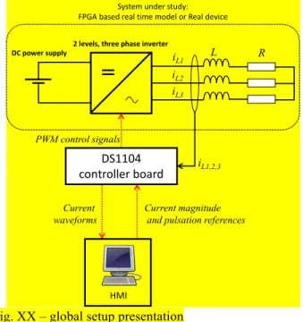
Figure


Documents relatifs
We present a configurable hard- ware architecture for a simple time manager implemented on an FPGA circuit, connected to a CPU executing the Xeno- mai framework in an embedded
Real-time and embedded systems dedicated UML modeling components developed within the OpenDevFactory project are used and combined to describe the deployment of the testbed control
Using this paradigm, the switch is modeled as a short circuit when in the on-state, and as an open circuit in the off-state. Once the state of all the switches, also called
For the component-based design, we propose three different configuration scenarios for the RTOS and the application presented in the preceding sections: the highly flexible,
We described in this paper the short-term and long-term evolution of the FTS real-time executive, making it an open server and adding new features such as partitioning tools for
Max is now based on the FTS client/server communication protocol, and uses the FTS class information protocol to obtain informations about FTS objects; this means that external
Ainsi, l' échantillon le moins sévère sur le plan symptomatique serait motivé de façon externe sociale dans l' adoption de comportement perfectionniste, alors que
Actuellement, nous savons que des perturbateurs endocriniens peuvent être retrouvés dans les produits cosmétiques.. Or, les PE peuvent avoir des effets à vie voire même engendrer
