OATAO is an open access repository that collects the work of Toulouse
researchers and makes it freely available over the web where possible
Any correspondence concerning this service should be sent
to the repository administrator:
[email protected]
This is an author’s version published in:
http://oatao.univ-toulouse.fr/24319
To cite this version:
Miquelot, Adeline
and Debieu, Olivier
and Rouessac, Vincent and
Villeneuve, Christina and Prud'homme, Nathalie and Cure, Jérémy and
Constantoudis, Vassilios and Papavieros, George and Roualdes, Stéphanie and
Vahlas, Constantin
TiO2 nanotree films for the production of green H2 by
solar water splitting: From microstructural and optical characteristics to the
photocatalytic properties. (2019) Applied Surface Science, 494. 1127-1137.
ISSN 0169-4332
TiO
2
nanotree
films for the production of green H
2
by
solar water splitting:
From
microstructural and optical characteristics to the photocatalytic
properties
Adeline
Miquelot
a,
Olivier Debieu
a,
Vincent Rouessac
b,
Christina Villeneuve
c,
Nathalie
Prud'homme
d,
Jérémy Cure
e,
Vassilios Constantoudis
f,g,
George Papavieros
f,g,
Stéphanie
Roualdes
b,
Constantin Vahlas
a,⁎aCirimat, 4 allée Emile Monso, BP-44362, 31030 Toulouse Cedex 4, France
bIEM, Université de Montpellier, CC 047 - Place Eugène Bataillon, 34095 Montpellier Cedex 5, France
cLaplace, Université Toulouse 3 - Paul Sabatier, 118, route de Narbonne - bât 3R3 -, 31062 Toulouse cedex 9, France dICMMO, Université Paris Sud, 11-SP2M-Bât, 410-91405 Orsay Cedex, France
eLAAS, CNRS, Avenue du Colonel Roche, 31031 Toulouse, France
fNCSR Demokritos, Neapoleos 27 and Patr. Grigoriou str., 15310 Aghia Paraskevi, Attiki, Greece
gNanometrisis, ΤEPA Lefkippos, Patriarchou Grigoriou & Neapoleos 27, PO Box 60037, Agia Paraskevi 15341, Attiki, Greece
A R T I C L E I N F O
Keywords: Solar water splitting TiO2 Nanostructure Photocatalysis Conductive-AFM MOCVD A B S T R A C T
Green H2production by solar water splitting relies entirely on the intrinsic properties of the photocatalyst. In this
study the impact of these intrinsic properties on the photocatalytic activity of anatase TiO2, the quintessential
component of state of the art photocatalytic systems was explored at the nanoscale. The exploration involved a holistic microstructural and optical characterization of fully crystallized anatase thin films synthetized by me-talorganic chemical vapor deposition. A combination of electron microscopy, spectroscopic ellipsometry, and infrared spectroscopy revealed that when the deposition temperature increased, the morphology evolved from dense to porous and columnar nanostructures. Interestingly, the columns with a complex, tree-like nanostructure photogenerated 18 times more H2than the densest sample. This result shows that the beneficial effect of the
morphological nano-complexification and crystallographic diversification of the exchange facets on the photo-catalytic performance outweighs the detrimental aspects inherent to this evolution, namely the drop of the charge carrier transport and the increase of residual stress.
1. Introduction
Research on renewable energy is vital in the current context of global warming and societies that rely on high energy consumption. Hydrogen is a promising source of renewable energy and catalyzed solar water splitting (SWS) is a carbon-free method to produce it. Numerous materials have been tested to catalyze this reaction [1,2]. Among them, TiO2 – because it is non-toxic, chemically stable,
abundant and affordable has been widely investigated as a photo-catalytic material since Fujishima and Honda's seminal work [3–8]. Despite its high energy band-gap (3.2 eV), crystalline anatase TiO2
shows attractive opto-electronic properties. It is an indirect semi-conductor with a long exciton lifetime [9,10]; it has a conduction band minimum energy level below the redox potential of H+/H2(0 V vs.
NHE) and a valence band maximum energy level above the redox po-tential of O2/H2O (+1.23 V vs. NHE) [11,12]. In contrast with powders,
Abbreviations: SWS, solar water splitting; ALD, atomic layer deposition; MOCVD, metalorganic chemical vapor deposition; TTIP, titanium tetraisopropoxide; FESEM, field emission scanning electron microscopy; EBSD, electron backscatter diffraction; GIXRD, grazing incidence X-ray diffraction; PF-QNM, peak force quantitative nanomechanical; C-AFM, conductive atomic force microscopy; SE, spectroscopic ellipsometry; SEP, spectroscopic ellipsometric porosimetry; HRTEM, high resolution transmission electron microscopy; MUD, multiples of uniform distribution; LO, longitudinal optical; TO, transverse optical; CL, correlation length
⁎
Corresponding author.
E-mail addresses: [email protected](A. Miquelot), [email protected](O. Debieu), [email protected](V. Rouessac),
[email protected](C. Villeneuve), [email protected](N. Prud'homme), [email protected](J. Cure),
[email protected](V. Constantoudis), [email protected](G. Papavieros), [email protected](S. Roualdes),
[email protected](C. Vahlas).
1 Torr fixed pressure, at different Tdranging from 325 to 500 °C, with
various durations that are adapted to produce films of similar thick-nesses (~350 nm).
Film composition is investigated by X-ray photoelectron spectro-scopy (XPS). The photoelectron emission spectra are recorded using a monochromatized Al Kα(hν = 1486.6 eV) source on a ThermoScientific
K-Alpha system with a 400 μm X-ray spot size. Depth profiling is per-formed by means of Ar+ion etching under 2 keV.
The crystal structure is investigated by XRD in a Bruker-D8 dif-fractometer equipped with a Cu Kα (λKαCu= 0.154 nm) anode in
theta-theta mode with a −3° offset. In addition, GIXRD is used to determine residual stress using a 4-circles goniometer (Panalytical X'Pert) equipped with a Cu anode (λKαCu= 0.154 nm) at 40 kV and 40 mA,
with Soller slits to get a nearly parallel beam, and a fast recording detector (X'celerator, Panalytical). The sin2ψ method (11 ψ angles ranging from −60° to 60°), in one direction (ϕ = 0°), was applied to the samples deposited on fused silica substrates. The {020} family plane (2θ = 48.08°) is analyzed from 45.7° to 51.2° with a 0.066° step, with the step time varying between 2000 and 2700 s depending on the sample. The XRD penetration depth is estimated at 100 nm for dense TiO2. The modus operandi to determine the strain from XRD
measure-ments is explained in the Supplementary Information (SI section 1). EBSD measurements are performed in a FESEM Jeol JSM 7100F TTLS LV on the sample surface to explore crystalline orientation. 8633, 4604, and 7888 points are measured on the 500 °C, 400 °C, and 325 °C samples, respectively, on 38 μm2surfaces. Because each grain is probed
only once to avoid overrepresentation of one grain orientation, the distribution remains statistical. Mid-IR (MIR) FTIR and far-IR (FIR) FTIR spectra are recorded by Perkin Elmer Frontier, and Nicolet iS50 ThermoFischer Scientific spectrometers, respectively. Films deposited on fused silica are investigated by transmission, total and diffuse re-flectance spectroscopy in the 200–1650 nm spectral range, using an Agilent-Cary 5000 spectrophotometer equipped with an integrating sphere. Samples deposited on Si coupons are analyzed by spectroscopic ellipsometry (SE) in the same spectral range with an incidence angle of 75° using a Semilab SE-2000 apparatus. Spectroscopic ellipsometric porosimetry (SEP) is performed with a Semilab GES5E spectroscopic ellipsometer (250–1000 nm) coupled with a lab-made cell in which ethanol pressure is increased step by step to progressively acquire el-lipsometric data adsorption isotherms in almost steady state. Before any data acquisition, the cell is pumped down to 50 mTorr, whereas the sample is heated up to 200 °C in the vacuumed cell for several minutes for a complete desorption from the TiO2film. The ellipsometry data are
analyzed on the energy range 1.24–4.25 eV by the Semilab SEA soft-ware using a two-layer architecture. A Cody-Lorentz oscillator model is used to describe the optical properties of the film, and a Bruggeman effective medium approach is chosen to simulate the surface roughness. With this full optical model, the regression goodness of fit in this range is over 0.98. The Cody-Lorentz model enables us to probe band-to-band transitions at the optical band edge and above the band edge, as well as band tails in the transparent spectral domain.
Top view and cross sectional scanning electron microscopy (SEM) micrographs of the Pt-metalized samples are obtained with a field emission FESEM Jeol JSM 6700F instrument. Before analyzing top view SEM images with the nanoTOPO_SEM™ software provided by Nanometrisis, they are processed to normalize the contrast of their il-lumination. Transmission electron microscopy (TEM) and high resolu-tion TEM (HRTEM) data are obtained with a JEOL JEM 2100F micro-scope. TEM specimens are prepared using a FEI Helios Nanolab600i dual beam SEM FIB (focused ion beam). The ion column is operated at 30 kV for all steps except final cleaning of the specimen, where a vol-tage of 5 kV and 2 kV is used. Beam currents vary between 47 nA and 15 pA. The electron beam is used to deposit a layer of C 200 nm thick over an area of 20 μm × 2 μm. The ion beam was then used to deposit a layer of Pt 3 μm thick over the same area. The sample was lifted out in situ and then attached to a copper support grid. Thinning of the specimen anatase TiO2 films can be used in photocatalysis as well as in
electro-photocatalysis. They are produced by various methods: sol-gel [13],
anodization [14], reactive magnetron sputtering [15], atomic layer
deposition (ALD) [16] or metalorganic chemical vapor deposition
(MOCVD) [4,17,18]. This last process interestingly enables the
pro-duction of various hierarchical morphologies that have an impact on the photocatalytic properties [5,19].
One way to efficiently control the morphology is the deposition temperature (Td), which allows obtaining nano- or microstructures that
range from dense to columnar [20–22]. Such Td induced
nanos-tructuration results in the increase of the specific surface area and therefore enhances the photocatalytic activity [23]. However, an
in-crease in Td can concomitantly affect other properties, such as the
texture, the electrical transport, the residual stress, and the nature of the external crystallographic facets in contact with the aqueous solu-tion. These factors can either enhance or be detrimental to the photo-catalytic activity [23–27]. Other aspects such as the stoichiometry can
also influence the photocatalytic performance through the subsequent modification of the electronic properties.
A significant number of results has been reported on the determi-nation of the morphology [16,18,28,29], the crystallographic phases
[22], the mechanical residual stress [26,30], the purity [2], the
elec-trical transport [9], and the optical band-gap [31]. However, there is no
systematic, holistic study of TiO2 films in the context of a strong
mor-phology evolution that connects all of these characteristics to the evo-lution of their photocatalytic properties. The present work thus, focuses on an extended characterization of MOCVD anatase TiO2 films in order
to investigate their photocatalytic behavior and thereby improve the photocatalytic performance by monitoring deposition parameters. The outcomes of this work can be extended to nanostructured TiO2 films
synthesized by other techniques.
We deposit TiO2 films by thermally activated MOCVD from titanium
tetraisopropoxide (TTIP) at six temperatures between 325 and 500 °C. We quantify the surface morphology of the deposited films through image processing and analysis of field emission scanning electron mi-croscopy (FESEM) micrographs. We apply, for the first time, electron backscatter diffraction (EBSD) to determine the growth direction of the anatase films. We determine the intrinsic mechanical residual stress of the films and their evolution with Td by grazing incidence XRD
(GIXRD), and we probe the mechanical properties at the nanoscale by peak force quantitative nanomechanical (PF-QNM). The electrical properties are investigated at the nanoscale by conductive atomic force microscopy (C-AFM) and at the macroscale by Hall effect measure-ments. We fit spectroscopic ellipsometry (SE) measurements using the Cody-Lorentz model [32], a powerful tool to determine the thickness,
the band-gap, and the refractive index that is affected by the porosity. We correlate the outcome of this comprehensive microstructural, electrical, electronic, and optical study with the photocatalytic activity measured by two techniques. First, we measure the photodegradation of stearic acid catalyzed by the TiO2 films by Fourier transform
infra-red (FTIR) spectroscopy, which is a variant of the Pilkington test [33–35]. Second, we measure the H2 photogeneration under Xe lamp
irradiation in a controlled atmosphere by gas chromatography [36]. 2. Material and methods
TiO2 films are deposited in a vertical, cylindrical, stagnant flow cold
wall stainless steel MOCVD reactor, which has been described in detail elsewhere [37]. In each experiment, P light-doped (1–20 Ω.cm) and As
high-doped (0.001–0.005 Ω.cm) n-type Si (100) wafers, and fused silica windows (Neyco) are placed on the heated sample holder. Titanium tetraisopropoxide (TTIP, 99.999%, Sigma-Aldrich) is conditioned in a double-walled glass bubbler and is thermally regulated at 20.5 °C. Pure nitrogen (99.9999% Messer) is used as both the carrier and dilution gas, and their flow rate is fixed to 4.7 and 52.4 sccm, respectively. All gas lines are thermally regulated at ca. 65 °C. Depositions are performed at
(a
) u.) (a. ty nsi te In
In te nsi ty (a. u.) (2 2 0 ) (b ) 2 θ (° ) 3 2 5° C 3 5 0° C 3 7 5° C 4 0 0° C 4 5 0° C 5 0 0° C (1 0 1 ) (1 1 2 ) (0 2 0 ) (1 2 1 ) (2 2 0 ) (1 2 5 ) (0 3 1 ) D e n si , e s (M UD ): 7 5 3 1 {1 0 0 } {1 1 0 } {0 0 1 } M in = 0 ,0 1 M a x = 8 (c ) 2 θ (° ) 3 0 4 0 5 0 6 0 7 0 8 0 6 5 7 0 7 5 Y X Z 0 ° 9 0 ° 4 5 ° 9 0 ° 45 ° 5 0 0 °C 4 0 0 °C 3 2 5 °C Fig. 1. (a) XRD patterns of TiO 2 fi lms deposited on SiO 2 substrates vs Td , the inset (b) presents an enlargement of the (220) peak. (c) EBSD pole fi gures of samples deposited at 325, 400 and 500 °C.
could proceed using a gradual cross-section cleaning milling pattern, with a final milling beam current of 80 pA. Finally, a 5 kV and 2 kV cleaning steps were carried out on each side.
Surface topography is probed by a Bruker Multimode 8 AFM ap-paratus in PF-QNM mode with Si-tip (Tespa-V2, Bruker). The me-chanical deformation is mapped using maximum contact force of ca. 65 nN. The tip sensitivity and its spring constant k are determined by force distance curve on Si reference wafer and by thermal tune, respectively. The vertical nanoscale charge transport is locally probed on thin films deposited on highly doped Si wafers by the AFM in conductive mode using a SCM-PtSi (Bruker) tip. A contact force of 27 nN and a sensor sensitivity of 100 nA/V are used. Hall measurements are conducted in a DC magnetic field with AC current from a Keithley 6221 current source and with an amplifier MFLI from Zurich Instruments. The contacts are Cu/Be and the injected current is of the order of 10−7 A.
The normalized Pilkington tests follow the photodegradation of stearic acid under UV–visible light (above 355 nm), as described else-where [28]. The relative quantity of stearic acid on the TiO2 films is
analyzed every 20 min by following the most intense stearic acid FTIR peak intensity evolution. For each sample, the test is repeated once after water cleaning. After the first run, the 500 °C film is delaminated, in contrast with the others which present perfect integrity. Finally, TiO2
induced water photodissociation tests are performed in a quartz reactor filled with a water-ethanol solution (1:1 vol) under Xe-lamp (300 W) illumination. The produced H2 quantity is measured every 6 h with a
gas chromatography apparatus connected to the photodissociation re-actor (PlotQ column (30 m) and PE-molisieve column (30 m); thermal conductivity detector; carrier gas: Ar).
A substantial effort has been made to ensure that only the final analysis for each sample is destructive or potentially destructive. To this end, both H2 photogeneration and stearic acid photodégradation are
realized on different samples for each Td, which have not been exposed
to other destructive analyses. 3. Results
3.1. Crystallographic phase and texture
The composition of the TiO2 films, which was determined on a
preliminary basis by XPS, showed no other contamination than the classical surface carbon due to adsorption of organic molecules, as re-vealed by the depth profiles.
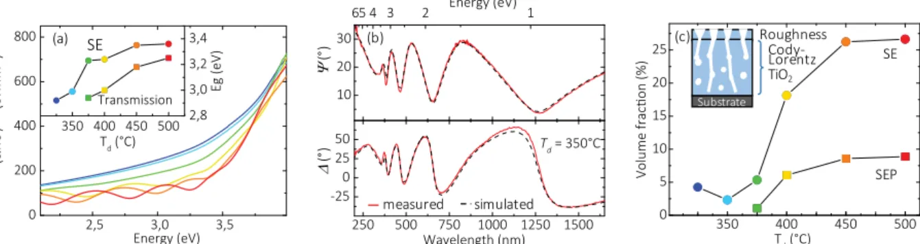
Fig. 1a shows XRD patterns obtained in a theta-theta mode, of ca. 350 nm TiO2 films deposited on SiO2 substrates at the different Td. In
this figure, and in the rest of the text, the following color coding is used: dark blue, light blue, green, yellow, orange, and red for Td of 325, 350,
375, 400, 450, and 500 °C, respectively.
Peaks measured at 25.4, 38.5, 48.1, 55.1, 62.7, 70.3, 75, and 76° correspond to the (101), (112), (020), (121), (024), (220), (125), and (031) crystallographic planes of anatase, respectively, according to the 99-100-9704 JCPDS powder card depicted for comparison. No peak from rutile or brookite is detected. All diffractograms present different intensity ratios than the powder reference pattern (shown in black), revealing textured films. Diffractograms of films deposited between 325 °C and 400 °C are rather similar, with two major peaks (101) and (020) that increase slightly with increasing Td. By contrast,
diffracto-grams, of films deposited at 450 °C and 500 °C show a general and significant intensity decrease, along with a change in peak ratio. The (101) and (020) peaks vanish while the (112) and the (220) (Fig. 1b) peaks increase.
Khalifa also reports a general decrease of XRD peak intensity with increasing Td, especially above 400 °C, for TiO2 films deposited by
MOCVD in similar conditions [22]. In this temperature range, a change
also occurs in the relative intensities between the (101) and (112) peaks, with the latter becoming predominant. The author attributes this behavior to the decrease of the migration length of the precursor
reveal any other crystal phase. The evolution of the TO3peak intensity
with increasing Tdremains the same as previously described for normal
incidence FIR measurements. In addition, LO3peak intensity decreases
as well, but to a lesser extent, resulting in the increase of the LO3/TO3
peak intensity ratio. In addition, a shoulder is observed at ca. 750 cm−1,
which can be related to the contribution of the LO2. The evolution of
the LO bands may be connected to the change in texture observed by EBSD and could suggest that high Tdsamples have an orientation of the
crystallites that favors the LO probe [41]. Moreover, with increasing Td
the LO3 peak shifts progressively from 866 cm−1 to 842 cm−1, as
highlighted by the arrow, with a concomitant increase of the LO3/TO3
intensity ratio. This is not discussed in the literature for TiO2; however,
Primeau et al. observed a drop of the LO3/TO3intensity ratio and an
inherent blue-shift of the LO3band with an increase in the annealing
temperatures of SiO2samples [42]. This behavior could be related to
the densification of the structure and the decrease of disorder. There-fore, the observed LO3red-shift and the increase of the LO3/TO3
in-tensity ratio with increasing Tdcan be explained by the increase in
porosity and by the subsequent impact on density and disorder. Another indirect indication of the increase in the porosity is a broad and weak band inFig. 2c, centered at ca. 3300 cm−1, which corresponds to the
stretching vibration of un-dissociated water [43,44]. The broad band intensity is globally higher for the high Tdsamples, because of their
highest porosity (as previously shown by the emergence of the
3900 3600 3300 3000 2700 0,0 1,0E-4 2,0E-4 A b s. /T h ic k. ( n m -1 ) 600 500 400 300 0,0 1,0E-3 2,0E-3 3,0E-3 A b so rb a n ce / T h ic kn e ss ( n m -1 )
(a) FIR non-,lted
260 440 Wavenumber (cm-1) TO3 TO1 TO2 ~340 325 C 350 C 375 C 400 C 450 C 500 C 900 800 700 600 500 0,0 3,0E-4 6,0E-4 9,0E-4 1,2E-3 Abso rbance / Thickness (nm -1 ) (b) MIR ,lted LO3 ~855 TO3 ~440 LO2 ~750 (c) MIR non-,lted
Fig. 2. FTIR spectra of films deposited at different Td. (a) Normal incidence FIR
spectra, (b) 70° tilted MIR spectra (c) Normal incidence MIR spectra.
molecules with increasing Td, which subsequently allows less time for
entities to arrange themselves in dense structures and leads to the in-crease of the nucleation rate. A high Td would favor the formation at the
surface of the (112) plan, less dense than (101), and would explain the change of the texture [22]. Alternatively, the observed changes in the
XRD pattern are attributed to the decrease of the c/a ratio arising from the near transition from anatase to rutile [38]. This possible initiation
of change of phase and texture could explain the general decrease in intensity of the XRD pattern with increasing Td. To further investigate
the change of texture, EBSD analysis was performed on three samples deposited at 325 °C, 400 °C, and 500 °C, respectively. The EBSD pole figures are presented in Fig. 1c with the substrate surface in the XY plane. Color mapping (same color level for all maps) represents the multiples of uniform distribution (MUD), in which a high value in-dicates a special orientation of the corresponding crystallographic plane. The low Td, densely structured films present a 〈100〉 growth
direction, revealed by the MUD value of 5 in the center of the corre-sponding pole figure. However, if the growth was following only the 〈100〉 direction, it would result in an additional signal pointing at ca. 90° in the same pole figure, the two signals corresponding to the < 100 > and 〈010〉 directions, equivalent in the tetragonal system. The absence of this feature means that at least one additional texture component exists, with another growth direction whose Miller indexes are different from 0 and 1. Nevertheless, the inference that < 100 > is one of the main growth direction at low Td, is in accordance with the
evolution of the XRD patterns vs Td in Fig. 1a, which show that the
(020) peak (corresponding to the < 100 > direction in the tetragonal system) is the most intense at low Td. The intermediate Td sample
(400 °C) does not present any MUD value higher than 3, indicating a transient regime with weak texture. This could be explained by a transition state between low- and high-Td films. In contrast, the highest
Td sample (500 °C) shows a 〈110〉 growth direction. The corresponding
most intense MUD value of 8 reveals the strongest texture among all samples. This evolution is consistent with XRD results in Fig. 1b, which show that the intensity of the (220) peak increases with increasing Td
and reaches a maximum at 500 °C. There is strong evidence of at least one more texture component in this sample. Indeed, the {110} pole figure shows not only the central disk and a circle at ca. 90°, both be-longing to the texture component already mentioned, but also a sup-plementary ring at ca. 25°. Furthermore, the {001} pole figure shows a ring at ca. 50°, in addition to the ring at ca. 90° that belongs to the first texture component.
Fig. 2a shows the FIR-FTIR spectra of the TiO2 films normalized by
their thicknesses as a function of Td. The FIR transmission spectra were
obtained with normal incidence. The spectra present peaks at 260 and 440 cm−1, which correspond to the anatase transverse optical phonons
TO1 and TO3, respectively, as reported by González et al. [39]. Two
broad shoulders centered at ca. 340 and 400 cm−1 are noticeable. The
first shoulder corresponds to the TO2 contribution. With increasing Td,
the TO1 and TO3 bands experience a general broadening, corresponding
to the greater contribution of the previously mentioned shoulders, and an intensity decrease resulting from the increase in the porosity. Therefore, the TO2/TO1 intensity ratio increases.
Moreover, a third shoulder emerges at ca. 520 cm−1 at 375 °C and
above. The increase of the intensity of this broad shoulder with in-creasing Td is explained by the progressive increase of voids among the
crystallites [29].
Fig. 2b shows MIR-FTIR spectra with an incidence angle of 70°. This configuration enables probing the longitudinal optical (LO) modes, which have a wave vector perpendicular to the film surface, in addition to the TO modes. This phenomenon, known as Berreman effect, has been highlighted by Trasferetti et al. [40] to identify the LO and TO
bands of anatase, rutile, and amorphous TiO2. In the present case, the
FTIR analysis shows that the films are composed of anatase only, with two major peaks around 440 cm−1 (TO
3) and 855 cm−1 (LO3), in
porosity. In contrast with CL, which already reaches a plateau at 375 °C, the spatial periodicity saturates only at the end of the morphological transition when the compact structures have been completely elimi-nated and the vertical columns cover the whole surface. This is due to the method of evaluating the spatial periodicity, which is sensitive to the presence of large features when mixed morphologies, composed of compact and columnar structures, co-exist. Complementary to CL, which marks the beginning of the surface morphological transition at 375 °C, the spatial periodicity is an indicator of the end of the transition
400°C 400°C 375°C 375°C 350°C 350°C 325°C 325°C 500°C 200 nm 500°C 450°C 450°C (a) (b) (g) (h) (i) (c) (d) (j) (k) (e) (f) (l)
Fig. 3. FESEM images of samples deposited at different Td, (a–f) plan-view on
the left, (g–l) 25° tilted cross-sections on the right. The scale bar is the same for every images.
520 cm−1 contribution), which results in a higher amount of water
adsorbed on the surface.
The crystallinity of the highest Td sample was investigated by TEM
as follows: the diffraction pattern of a selected area was divided in six sections and the six resulting dark field images were superimposed (Fig. S1, SI). Since bright parts are crystalline (and well oriented) in dark field images, if a dark part is crystalline on the superimposition image, then every brighter section is crystalline as well. For this reason, the area in the small black square on the figure, which is one of the darkest parts of the probed sample zone, was investigated by high resolution TEM (HRTEM). Its fast Fourier transform, also presented in Fig. S1b (SI), reveals diffraction spots corresponding to the crystallographic planes of anatase. It is thus concluded that the entire area and, conse-quently, the film as a whole (considering the good homogeneity of the sample), is crystalline. Fig. S2b–c (SI) shows the diffraction pattern of two encircled areas of the dense lowest Td sample (325 °C) and Fig.
S2b–c (SI) shows the summit of a grain and its crystallographic plans: both reveal that this film is entirely crystalline.
3.2. Morphology
The morphological evolution of the TiO2 films with Td is studied by
FESEM. Fig. 3 presents top-down (left) and 25° tilted cross-sectional (right) FESEM micrographs of the TiO2 films. With increasing Td, both
surface and cross-sectional micrographs show a decrease in the size of the various structures, with morphologies evolving from dense and angular structures to isolated and nanostructured tree-like columns. It is noticeable that the films deposited at 325 and 350 °C show similar morphologies, and the same holds for those deposited at 450 and 500 °C. The transition from compact to columnar morphology is in-itiated at 375 °C, as shown by the subdivision of grains on the top-down micrograph (left). The morphology evolves further at 400 °C, at which point a rather disordered columnar structure emerges. The evolution of the morphology with the increase of Td is accompanied by a significant
increase in the porosity: at 375 °C, it is manifested only between grains, whereas at 400 °C and above, it is also manifested in the small features that can be observed within the columns. Therefore, the specific surface area of the films increases considerably with increasing Td.
Images were analyzed with the nanoTOPO_SEM™ software (Fig. 4) to achieve a quantitative description of the film morphology. Fig. 4a shows the evolution of the correlation length (CL) and the spatial per-iodicity, which are related to the grain size and density, with Td. Fig. 4b
shows the evolution of skewness and kurtosis, which are related to the porosity.
The CL describes distances with pixels of same grey levels on the FESEM images. Therefore, in the present case, it depends on the grain size and illustrates its evolution. With increasing Td, CL decreases
drastically from 67 nm at 325 °C to 13 nm at 375 °C, and then reaches a plateau. This behavior is attributed to the co-existence of two grain sizes in the surface morphology of films deposited between 350 and 450 °C. Since CL is calculated from the short-distance behavior of the autocorrelation function of image pixels, it is more sensitive to the smaller size: consequently, in the present case, it captures the very first appearance of the columnar structure in surface morphologies at 375 °C.
The spatial periodicity is calculated from the inverse of the spatial frequency, which corresponds to the more prominent peak of the Fourier transform of the FESEM image. For samples deposited at 325 and 350 °C, which are characterized by closely packed structures, the spatial periodicity value is ca. 500 nm. This evaluation of the size of the repeat unit corresponds to the width of a pack with different local elevations. Increasing Td results in an overall decrease in the spatial
periodicity. Stabilization occurs for the samples deposited at 450 and 500 °C: ca. 88 nm. In this case of discrete surface features, this value describes the mean distance between one side of a column and the equivalent position on the next column, including the inter-columnar
that occurs at 450 °C.
Skewness and kurtosis (Fig. 4b) are two parameters describing the shape of the grey level histogram of images. Kurtosis describes the flatness of the histogram, thereby discriminating the case in which there is a strong contribution of the dark and light pixels (kurtosis < 3) from the images in which the vast majority of pixels is around the mean grey level (kurtosis > 3). Kurtosis values are higher than 3 for the three samples deposited between 325 and 375 °C, corresponding to a sig-nificant contribution for these samples from mean grey pixels, and consequently to relatively flat surfaces with small local slopes. For the three samples deposited at the highest Td, kurtosis values are lower than
3 because of the greater contribution of brighter pixels (corresponding to the extremities of columns) and darker pixels (corresponding to the porosity among columns). Skewness characterizes the symmetry of the histogram; i.e. whether the darker (skewness < 0) or the lighter (skewness > 0) pixels are the more prominent. It becomes negative above 375 °C, revealing the gradual darkening of the micrographs that marks, the emergence of the inter-columnar porosity.
Fig. 4c illustrates the evolution of the arithmetical mean deviation (Ra) and the root mean squared (Rq) roughness of the assessed profile
with increasing Td. The Raand Rqof films deposited at 325 °C equal 33
and 42 nm, respectively. These values show consistent evolution, i.e. they monotonically decrease with increasing Tdand are stabilized at
5 nm at 450 °C and above. A complementary approach to the estimation of the roughness is provided by SE analysis, where roughness is simu-lated by a surface layer composed of a volume fraction of void and of TiO2following the Bruggeman effective medium approximation.Fig. 4c
also shows the evolution of the thickness of this roughness layer vs Td.
The thickness is 40 nm at 325 °C, which then decreases to 28 nm at 375 °C and finally increases to reach the maximum value of 42 nm at 500 °C. Whereas the three lowest Tdsamples give consistent roughness
results regardless of the probing technique (photons or mechanical probe), the values for the columnar samples depend strongly on the probing method, namely on its depth sensitivity. SE analysis seems to take into account the beginning of the inter-columnar void below the summits, in contrast with the AFM tip, which cannot probe the porosity among adjacent columns at a fine scale.
To obtain a deeper insight into the morphology of the columnar 500 °C film, we compare TEM and FESEM micrographs inFig. 5. The sample is 15° tilted in the plane of the images on all TEM images. The FESEM cross-section image,Fig. 5a, shows bottom-up oriented, cypress-like columns, illustrated by the inset scheme. The surface micrograph of
Fig. 5b shows compact triangular superstructures, which are
300 350 400 450 500 0 10 20 30 40 R a & R q (n m ) 2,50 2,75 3,00 3,25 3,50 -0,4 -0,2 0,0 0,2 0,4 K u rt o si s S ke w n e ss 20 40 60 80 100 200 300 400 500 C o rr e la , o n l e n g th ( n m ) S p a , a l p e ri o d ic it y (n m ) Ellipsometry AFM (a) (b) (c) Transi,on start Transi,on end R o u g h n e ss th ic k n e ss (n m ) Td(°C) Ra & Rq
Fig. 4. FESEM images analysis parameters vs Td. (a) Correlation length (CL) and
spatial periodicity. (b) Kurtosis and skewness. (c) AFM Raand Rqroughness
values, and ellipsometric roughness vs Td.
1 00 nm 1 00 nm (b ) (a) 5 0 nm 1 00 nm 1 0 nm 1 0 nm (g) (h ) (c ) (d ) (e) (f)
Fig. 5. Electron microscopy images of the 500 °C anatase film. (a) Cross-section FESEM image. (b) Top-view FESEM image. (c–d) Cypress-like TEM image. (e–f) Fir-like TEM image. (g) HRTEM of the cypress-Fir-like summit. (h) HRTEM of the apparent conical-shaped summit.
different deformation areas remain, whereas at higher Td(450 °C and
500 °C) the deformation is homogenous over the surface. At low Td, the
diversity in mechanical responses is probably linked to small variations in the Young's modulus as a function of crystallographic orientation [45]. At high Td, we link the decrease in the diversity of deformation
areas to the general decrease in the grain size, which means that what is probed at higher Tdis the mechanical response of a group of
nanos-tructured tree-like columns with different crystallographic planes. It is also noticeable that the mean deformation under a fixed applied force increases globally with Td, i.e. with the change in morphology from
dense to columnar. This is compatible with the increase in the porosity within and between the grain, which enables easier deformation.
The residual stress of the films was investigated by GIXRD. For all samples, the residual stresses are compressive and increase from −150 ± 20 MPa at 325 °C to −300 ± 100 MPa at 450 °C, as shown in the inset ofFig. 6g. These values are low compared to the Young's modulus of bulk (195 GPa [45]) and the stress of anatase films reported in the literature for different deposition techniques (sol-gel: −2185 MPa [46], sputtering: −890 MPa [26], ALD: −700 MPa [45]). As mentioned in Section 2 of the SI, these anatase films are supposed to be quasi-isotropic and two stress origins can be considered: σg, the film
growth stress induced during the deposition and σth, the thermal stress
induced by the difference in the thermal expansion coefficients of the SiO2substrate and the TiO2film during cooling after deposition. The
residual stress can be a mixture of thermal and growth stress. For the films deposited, the estimates of thermal stress σthin the film range
between 798 and 1256 MPa, as shown in Section 2 in SI. Therefore, excluding the thermal stress, the growth stress for all the samples is strongly compressive, ranging between −948 and −1425 MPa. This compressive growth stress is very likely to ensue from the evolution of 70 nm -70 nm 3 nm 0 nm 30 nm -30 nm 2 nm 0 nm 50 nm -50 nm (a) (b) (c) (d) (e) (f) 325 °C 7 nm -2 nm 450 °C 375 °C 0 1 2 3 4 5 0 2 4 6 8 10 12 O cc u rr e n ce ( % ) Deforma,on (nm) 300 350 400 450 -400 -300 -200
Residual stress (MPa)
Td (°C) (g) 130 nA -700 nA 30 nA -140 nA 0 nA -50 pA 200 nm (h) (i) (j) (k) (l) (m) Voltage -5 V 200 nm Voltage -3,5 V Voltage -3 V 70 nm -70 nm 50 nm -50 nm 20 nm -20 nm
Fig. 6. (a–c) Evolution of topography and (d–f) deformation for three different Td, 325 °C (a, d), 375 °C (b, e) and 450 °C (c, f). (g) Mechanical aspects: influence of Td
on deformation occurrence, the insert shows the residual stress σ against Tdprobed by GIXRD. (h–j) Topographic maps corresponding to the current maps: (h) 325 °C,
(i) 375 °C and (j) 450 °C.
comparable with the top view scheme of cypress-like columns. Bottom-up oriented cypress-like columns are also visible in the TEM cross-section in Fig. 5c–d. However, in some rare cases, the layers of the structure are oriented toward the substrate, resembling a fir-like mor-phology as shown in Fig. 5e–f. We conclude that the layered structures present a wide range of orientations, with an apparent predominance toward the top. Fig. 5 (panels g and h) shows HRTEM micrographs of two columns, a cypress-like summit and an apparently conical one, which may represent the same structure from two different perspec-tives. All micrographs highlight the high specific surface of the 500 °C samples formed by such columnar morphology.
TEM analysis indicates that the column summits are monocrystal-line. In contrast with the low Td morphology composed of monolithic
grains, this 500 °C film morphology composed of a forest of tree-like nanostructures is far more complex. It exhibits small-scale details and large variability in the orientation of the films. Therefore, taking into account the different sides of each column and column layer, this im-plies that the columnar structure exhibits a higher diversity in the crystallographic facets at the surface than the dense films.
3.3. Mechanical characteristics
Fig. 6a–c presents the AFM surface micrographs of the 325, 375 and 450 °C samples. The observed morphology is in agreement with the FESEM images. Deformation maps of the same probed sample area for a maximum applied force of 65 nN are shown in Fig. 6d–f. Fig. 6g is the deformation occurrence diagram of the six samples. The dense 325 °C film exhibits a mechanical response to stress that differs from one grain facet to another, resulting in the observation of six main different de-formation areas (see the blue arrows). For intermediate Td, three
the morphology and texture. 3.4. Electrical characteristics
Fig. 6h–j shows the current maps of the TiO2samples deposited at
325, 375, and 450 °C, probed under negative voltage. The maps show a decrease in the maximum current (see the current scale on the right) with the increase of Td. However, these maximum values are related to
very small areas of the maps. Therefore, the mean values are more representative of the evolution of the electrical properties of the films. Under the same applied voltage of -3 V, they are −108, −6, and 0 nA for samples deposited at 325, 375, and 450 °C, respectively. They take into account the conductive area ratios, which are 50, 14, and 10%, respectively. The general decrease in charge transport with the increase in Tdfollows the appearance of the columnar structures and of the
in-crease in the porosity.
Hall effect measurements on samples deposited at 325 and 400 °C evidence the n-type character of the TiO2films. It is reasonable to
as-sume that the samples deposited at intermediate Td, i.e. 350 and 375 °C,
are n-type semiconductors as well. Furthermore, charge carrier density for the 325 °C sample is 1 ± 0.3 × 1018cm−3and that for the sample
deposited at 400 °C is 2.9 ± 0.2 × 1018cm−3. This increase implies a
decrease in the charge mobility, which can be attributed to the in-creased complexity of the morphology with the emergence of voids between and inside the nanostructures.
3.5. Optical characterization
In order to determine the optical band-gap Eg of the films, we plot in
Fig. 7a the Tauc plot of the absorption coefficient α for indirect semi-conductors. Despite the fact that all films present similar thicknesses determined by SE and by FESEM (295–435 nm), it is clear that inter-ference fringes below the optical absorption edge disappear for low Td
films (< 400 °C). This is because of light scattering caused by larger nanostructures above 300 nm that clearly emerge below 400 °C, as shown by FESEM and AFM (Fig. 3andFig. 6a–c). This is confirmed by the diffuse reflectance spectra showing a significant increase in in-tensity while Tddecreases to below 400 °C (Fig. S3a, SI). In addition, we
also analyze the optical properties below the band-gap by SE using the exponential Urbach formalism of the Cody-Lorenz model i.e. the slope Eu and the demarcation energy Etbetween the Urbach tail transition
and the band edge [47]. The evolution of Eu with Td(Fig. S4, SI) is the
inverse of the evolution of the reflected diffuse light intensity. There-fore, we can conclude that the loss of light in the transparent spectral domain is probably because of scattering and not because of Urbach states. Moreover, scattering seems to be the main cause of the reflec-tion, since the total (Fig. S3b Si) and diffuse (Fig. S3b.a SI) reflectance spectra are very similar in the UV range. At 285 nm, both spectra show a major increase with decreasing Td, from 8 to 27% and 0.5 to 25%
respectively. This means that at low Td, up to 25% of the intensity of
light is lost for the photocatalytic process because of scattering. The insert of Fig. 7a shows that Eg determined by transmission spectroscopy decreases monotonously from 3.25 at 500 °C, which cor-responds to bulk anatase, to 2.94 at 375 °C. Despite the difficulty of determining the optical band edge from the linear part of the Tauc plot because of interferences and scattering, this monotonous trend is si-milar to the one estimated by SE on the entire series (seeFig. 7a). A slight shift is observed between the two measurements, which has al-ready been observed with various Si alloys and may be inherent to the Cody-Lorentz model [47].
The decrease of Eg with decreasing Tdcould result from the
pro-gressive increase of the content of shallow donor levels caused by in-trinsic defects as oxygen's vacancies (Ov) and/or Ti3+oxidation states.
Valence band spectra from XPS measurements of samples deposited at 325 and 450 °C are similar, as shown in Fig. S5a (SI), which would point to an apparent downshift of the conduction band of low Tdsamples.
However, we do not detect any distinctive signatures of Ti3+or O vin
surface XPS spectra (Fig. S5b, c–h, SI). Indeed, the 531.8 eV contribu-tion can be related to oxygen from adsorbed carbon species or OH groups, as well as Ov [48]. Also, depth analysis with argon cluster
sputtering would induce a reduction effect that would bias the results. Moreover, Hall effect measurements show an increase in the con-centration of charge carriers with the increase of Td. Therefore, the
decrease in the optical absorption threshold with decreasing Tdcould be
partly related to the progressive increase of scattering (Fig. S3, SI). Nevertheless, the SE band-gap also decreases with Tddespite the use of
an Urbach tail contribution for the deconvolution of the scattering. This suggests that the band-gap may be narrowed with decreasing Td.
Fig. 7b shows the ellipsometric angles Ψ and Δ of the sample de-posited at 350 °C, and the simulated SE data using the film architecture displayed in the inset ofFig. 7c. It is worth noting the high fit quality in the transparent region and above the absorption edge. Furthermore, the refractive index n and the extinction coefficient k reported in Fig. S6 (SI) using the Cody-Lorentz model are similar to previous SE spectra used to analyze amorphous and crystalline anatase [32,49,50]. We observed an increase in n with decreasing Td(Fig. S6, SI). This increase
of n is caused by the rise in the density. Thus, the rise of the optical reflection (Fig. S3b Si), which is mainly due to scattering, is explained by the concomitant increase of the size of the nanostructures and the refractive index.
Fig. 7c shows the volume fractions of void (fvoid) vs Tdestimated
from n@633 nm of the films, and of bulk anatase following the Lorentz-Lorenz equation. In this case, fvoidis an estimate of the total porosity,
including the closed porosity, whereas the volume fraction of ethanol resulting from SEP corresponds only to the open mesoporosity with a maximum pore size of ca. 20 nm. We attribute the difference between the results to the fact that the large mesoporosity and macroporosity cannot be filled by ethanol by capillary condensation. The closed
250 500 750 1000 1250 1500 -25 0 25 50 10 20 30 Wavelength (nm) = 350°C 65 4 3 2 Energy (eV) 1 2,5 3,0 3,5 0 200 400 600 800 350 400 450 500 2,8 3,0 3,2 3,4 Energy (eV) Transmission E g ( e V ) T d (°C) SE measured simulated (° ) (° ) ( h ) 1 /2 (e v .n m -1) 1 /2 (a) (b) 350 400 450 500 0 5 10 15 20 25 Td (°C) V o lu m e fr a c, o n ( % ) Roughness Cody-Lorentz TiO2 Substrate (c) SE SEP
Fig. 7. (a) Tauc plot of the absorption coefficient determined by UV–Vis-Nir transmission spectroscopy for samples deposited at the different Td– the inset shows
films Egdetermined by UV–vis-Nir transmission spectroscopy and by SE. (b) Ellipsometric angles Ψ and Δ of the TiO2thin film deposited at 350 °C. (c) Porosity
porosity, inaccessible to ethanol, could be negligible in the porous structure. No model using effective medium approximations composed of void and crystalline and/or amorphous anatase could significantly fit the SE data, since it cannot accurately describe band-gap and scattering intensity variations. Therefore, the values reported inFig. 7c inset vs Td
are only indicative. However, the increase of both volume fractions with increasing Tdreflects the increase in porosity within and between
the nanostructures, which is apparent in the FESEM and HRTEM images (Fig. 5).
3.6. Photocatalytic evaluation
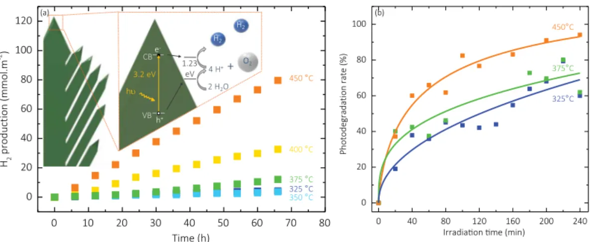
To study the evolution of the SWS photocatalytic properties of the TiO2 films vs Td, two tests were carried out. First, water
photo-dissociation rates are quantified by the cumulative H2 production. Fig. 8a shows the amounts of H2as a function of time produced by
photocatalysis by the films deposited between 450 and 325 °C, corre-sponding to the entire range of morphologies. All films display constant H2production throughout the 66 h of the analysis, as shown by the
linearity of the curves, revealing their high stability. Furthermore, the repeatability of the experiments has been established by testing a 450 °C sample thrice and acquiring the same results. After 66 h, the well-organized, nanotree-shaped TiO2 (450 °C) displays the highest
cumulative H2production of 78.9 mmol.m−2. After the same duration,
the TiO2 with disorganized columns (400 °C) shows a production of
only 36.2 mmol.m−2
, i.e. less than half of the production of the film deposited at 450 °C. The intermediate, 375 °C sample displays a pro-duction of 12 mmol.m−2and the two dense TiO
2 show similar
pro-duction quantities of 3.6 and 4.4 mmol.m−2
for 350 and 325 °C, re-spectively. The well organized columnar film shows the best photocatalytic performance, which is far better than the others. Com-parison of these results with the literature is difficult because of the diversity of the reported photocatalytic protocols used, in terms of so-lutions, protocol pressure, normalization, or intensity of the light source [51].
A second photocatalytic analysis was performed by the Pilkington test, shown inFig. 8b, following the photodegradation of stearic acid under UV-light illumination. The results of three samples (325, 375 and 450 °C) exhibiting the three characteristic morphologies are shown, revealing that the photocatalytic activity of the high Tdsample is better
than the 375 and the 325 °C ones. The highest photodegradation rate is close to the rate from PECVD-processed pure anatase TiO2film reported
by Zhou et al [34].
The straight hierarchy between the photodegradation rates of the three samples shown on the Fig. 8b can be attenuated by the other samples results (Fig. S7, SI) that show, for instance, that the 400 °C sample is more efficient than the 450 °C sample. Additional results on
Fig. S7 (SI) also show that initially, the sample deposited at 350 °C is more active than the one deposited at 325 °C.
Both analyses show the strong tendency of higher Tdsamples to
show higher photocatalytic activity. For H2photogeneration, there is
only one small exception to this trend – the samples deposited at 325 and 350 °C – since the former exhibits slightly better activity than the latter. However, as described earlier, several samples do not follow the trend for stearic acid photodegradation. These exceptions are not sur-prising when one considers the fact that competition among a number of properties and characteristics results in the final photocatalytic performance of the materials. This is especially the case given that the properties do not show a steady evolution with Td. For instance, this is
the case with the mean current probed by C-AFM, which shows a strong early decrease with the increase of Td, or for the evolution of XRD
patterns, in which significant change begins only at 450 °C. Moreover, the evolution of some properties is not quite monotonous: for example, the porosity as determined by ellipsometry between 325 and 350 °C. Finally, the initial amount of stearic acid on surface samples could be different from one sample to another because of specific surface dif-ferences between them, which could explain the fact that stearic acid photodegradation results show more exceptions to the general trend. Therefore, the 400 °C sample, which is less porous than the 450 °C one, could have less acid stearic to photodegrade in the first place. For all these reasons, we focus in the following discussion on only the general trend, which is indisputable.
4. Discussion
The strong increase in the morphological complexity of anatase films obtained with increasing Tdhas a positive impact on the
photo-catalytic performance. This impact can be analyzed by the following photocatalytic mechanisms: carrier photogeneration, carrier con-centration, carrier transport, and properties of the surfaces exposed to the aqueous catalytic solutions. Changes in the morphology of TiO2
films with increasing Tdhave been reported extensively in the
litera-ture. Taylor et al. [21] observed the same morphological evolution of MOCVD TiO2films from TTIP. According to them, the increase of Td
results in the decrease in the migration length of active species and in a concomitant decrease in the number of hops before reaction. Therefore, at low Td, reactive species have time to diffuse, which results in large
and compact structures, whereas high Tdfavors nucleation and leads to
preferential growth on pre-existing structures. This, in turn, leads to the formation of the columnar complex nanotrees, which GIXRD reveals to be compressed, and more subject to deformation under fixed applied force. This growth mechanism leads to highly porous films at high Td,
estimated to be ca. 26 vol% of void by SE. Further evidence is provided by FTIR, which shows a significant decrease in the number of TieO
0 40 80 120 160 200 240 0 20 40 60 80 100 ) %( et ar n oit a d ar g e d ot o h P
Irradia,on ,me (min)
+
2 H2O hυ CB VB e -450 °C 375 °C 325 °C (b) 450°C 375°C 325°C 350 °C 400°C 3.2 eV 1.23 eV 4 H + h+ O2 H2 H2 (a) 0 10 20 30 40 50 60 70 80 0 20 40 60 80 100 120 H2 m.l o m m( n oit c u d or p -2 ) Time (h)high Tdsamples to the strong increase in the specific surface area. This
increase is induced by spaces between the nanotree-like columnar structures and possibly by the smaller space within each column, which were observed by both FESEM and HRTEM, in accordance with FTIR analyses. We also observe a significant increase in the porosity with increasing Td. The maximum volume fractions of void corresponding to
the open mesoporosity (estimated by SEP) and full porosity (estimated by SE) were 9% and 26%, respectively. Moreover, we observe a de-crease in the optical reflection with increasing Td, which is mainly
caused by scattering and which may favor the photocatalytic process. In addition, the inherent increase in the diversity of the exposed crystal-lographic facets with the increase in the morphological complexity may have a positive impact on the H2 production performance as well.
Notably, we show for the first time by EBSD a change of one of the main growth direction: < 100 > at 325 °C and < 110 > at 500 °C. However, we observe a decrease of the charge mobility, which is detrimental to the photocatalytic performance, as could be the case with the increase in the residual compressive stress. Therefore, we have performed an extended investigation of the nanoscale electrical and electronic prop-erties with regard to the crystallographic propprop-erties of the nanotree-shaped TiO2. The results of this analysis will be published in a
forth-coming paper. Acknowledgements
This work was supported by funding from Toulouse Tech'Interlab and Association Instituts Carnot. The photocatalytic experiments were supported by the Université de Toulouse (IDEX MUSE).
We are indebted to Claire Tendero, Diane Samelor, Daniel Sadowski, Cédric Charvillat, Olivier Marsan, Jérôme Esvan, Benoît Malard, Bertrand Viguier, Alessandro Pugliara (Cirimat), Stéphane Leblond du Plouy, Arnaud Proietti, Claudie Josse (UMS Castaing) and Emmanouil Soulos (IEM) for their contributions to this work. Appendix A. Supplementary data
Supplementary data to this article can be found online athttps:// doi.org/10.1016/j.apsusc.2019.07.191.
References
[1] J. Yu, Z. Chen, L. Zeng, Y. Ma, Z. Feng, Y. Wu, H. Lin, L. Zhao, Y. He, Synthesis of carbon-doped KNbO3photocatalyst with excellent performance for photocatalytic hydrogen production, Sol. Energy Mater. Sol. Cells 179 (2018) 45–56,https://doi. org/10.1016/j.solmat.2018.01.043.
[2] W. Michael G., W. Emily L., M. James R., B. Shannon W., M. Qixi, S. Elizabeth A., L. Nathan S., Solar water splitting cells, Chem. Rev. 110 (2010) 6446–6473. doi:https://doi.org/10.1021/cr1002326.
[3] A. Fujishima, K. Honda, Electrochemical photolysis of water at a semiconductor electrode, Nature 238 (1972) 37–38,https://doi.org/10.1038/238037a0. [4] S.P. Krumdieck, R. Boichot, R. Gorthy, J.G. Land, S. Lay, A.J. Gardecka,
M.I.J. Polson, A. Wasa, J.E. Aitken, J.A. Heinemann, G. Renou, G. Berthomé, F. Charlot, T. Encinas, M. Braccini, C.M. Bishop, Nanostructured TiO2 anatase-ru-tile-carbon solid coating with visible light antimicrobial activity, Sci. Rep. 9 (2019) 1883–1893,https://doi.org/10.1038/s41598-018-38291-y.
[5] S.G. Kumar, K.S.R.K. Rao, Comparison of modification strategies towards enhanced charge carrier separation and photocatalytic degradation activity of metal oxide semiconductors (TiO2, WO3and ZnO), Appl. Surf. Sci. 391 ( (2017) 124–148,
https://doi.org/10.1016/j.apsusc.2016.07.081.
[6] T. Sharifi, Y. Ghayeb, T. Mohammadi, M.M. Momeni, Enhanced photoelec-trochemical water splitting of CrTiO2nanotube photoanodes by the decoration of their surface via the photodeposition of Ag and Au, Dalton Trans. 47 (2018) 11593–11604,https://doi.org/10.1039/c8dt02383b.
[7] M.M. Momeni, Y. Ghayeb, M. Shafiei, Preparation and characterization of CrFeWTiO2photoanodes and their photoelectrochemical activities for water split-ting, Dalton Trans. 46 (2017) 12527–12536,https://doi.org/10.1039/c7dt01596h. [8] M.M. Momeni, M. Mahvari, Y. Ghayeb, Photoelectrochemical properties of
iron-cobalt WTiO2nanotube photoanodes for water splitting and photocathodic pro-tection of stainless steel, J. Electroanal. Chem. 832 (2019) 7–23,https://doi.org/ 10.1016/j.jelechem.2018.10.035.
[9] H. Tang, K. Prasad, R. Sanjinès, P.E. Schmid, F. Lévy, Electrical and optical prop-erties of TiO2anatase thin films, J. Appl. Phys. 75 (1994) 2042–2047,https://doi.
org/10.1063/1.356306.
TO1–3 vibrations with increasing Td, by the concomitant drop in the
TO3/LO3 intensity ratio, which is also an indication of increasing
dis-order, and by the LO3 red-shift. The high porosity generated by the
nanotree structuration is mainly in the form of space between columns, as revealed by the analysis of the plan-view FESEM images and shown by the inter-columnar gaps in the cross-sectional FESEM and HRTEM images. This nanostructuration leads to nanotree morphologies, the most common of which exhibits branches directed toward the top, re-sembling a cypress. The conical shaped summits seem to belong to the same morphology but observed from a different side. This results in a high specific surface which is also evidenced by the appearance of the 520 cm−1 FTIR contribution. The change in the morphology of the TiO
2
films with increasing Td also results in a stronger crystallographic
tex-ture and in a change in the growth direction after a transitional step, as evidenced by EBSD, and potentially by FTIR [41]. Besides, HRTEM
suggests that the diversity and the number of the crystallographic facets exposed to the contact with the aqueous solutions for H2
photo-generation or with stearic acid for the Pilkington test increase sig-nificantly with increasing Td. Murakami et al. suggested that a balanced
ratio between (101) and (001) surfaces would improve the photo-catalytic performance by improving charge separation and, therefore, the lifetime of the excitons, because of the presence of both oxidative and reductive surfaces [52]. Such surfaces were confirmed by the work
of Yu et al. [53], and the oxidative character of particularly the (100)
surface was confirmed by Roy et al. [54]. Nevertheless, these studies
concern free nanocrystallites and not films composed of dense or porous structures, where charge carrier transport plays a more significant role in the photocatalytic properties. We observed that charge carrier transport decreases significantly with the strong nanostructuration of the morphology, and the decrease in grain size, as revealed by both C-AFM and Hall effect measurements. This is consistent with the work of Chen et al., who showed that the charge mobility of small anatase na-norods (0.57 cm2 V−1 s−1) [55] is much lower than that of large
crys-tallites (20 cm2 V−1 s−1) [9]. Further, we suspect that a larger number
of grain boundaries in the nanotree TiO2, which act as diffusion centers
[56], and a higher disorder may cause charge carrier traps and ohmic
behavior. Finally, the intensity of reflected light increases with in-creasing Td mainly because of scattering.
We witness here the competition among different effects involved in the photocatalytic performance of the TiO2 films with increasing Td.
The beneficial effects include the drop in the optical reflection, the increase in charge density, the huge enhancement of the exchange surface, and the higher diversity of the crystallographic facets. These effects overcome the detrimental effects, which include, potentially, the compressive residual stress [26,30], and the decrease in charge carrier
mobility. The latter effect may indicate that the redox reactions mainly involve excitons generated at the extreme TiO2 surface. As for the effect
of the potential narrowing of the optical band-gap, that could hinder the photocatalytic activity by decreasing the number of absorbed photons. However, the narrowing could also be beneficial: if this downshift is strong enough to position the conduction band below the H+/H
2 redox potential, the reduction reaction would be compromised.
By contrast, high Td samples would benefit from the thermodynamic
driving force arising from a suitable position of the conduction band [57], as shown in Fig. 8a.
5. Conclusion
We deposited anatase TiO2 films by thermal MOCVD. In this
pro-cess, increasing Td induces a strong increase in morphological
com-plexity through the formation of nanotree-like columnar structures. The positive impact of this change on the water-splitting performance is investigated. We observe a 66 h cumulative H2 production that
in-creases from 4.4 to 78.9 mmol.m−2 as T
d increases from 325 to 450 °C.
In the complex competition between the numerous properties affecting the photocatalytic mechanisms, we attribute the better activity of the