Pépite | Croissance localisée dans le plan des nanostructures III-V par épitaxie par jets moléculaires
140
0
0
Texte intégral
(2) Thèse de Maria Fahed, Lille 1, 2016. 2 © 2016 Tous droits réservés.. lilliad.univ-lille.fr.
(3) Thèse de Maria Fahed, Lille 1, 2016. Remerciements ___________________________________________________________________________ Je tiens d’abord à remercier Mr. Lionel Buchaillot, directeur de l’Institut d’Electronique, de Microélectronique et de Nanotechnologie (IEMN), de m’avoir permis de réaliser ma thèse au sein de cet Institut. Ce travail a bénéficié du soutien financier de la région des Hauts de France ainsi que des contrats ANR SAMBA et MOSInAs. Je remercie Mme Chantal Fontaine et M. Charles Cornet d’avoir accepté d’être rapporteurs de ce manuscrit, Mme Isabelle Lefebvre et MM. Gilles Patriarche, Clément Merckling et Sylvain Bollaert d’avoir accepté de faire partie de mon jury de thèse. Ce fut pour moi un honneur mais aussi un plaisir que de présenter mes travaux devant eux. Un grand merci à mon directeur de thèse Xavier Wallart, directeur de recherche à l’IEMN, pour sa confiance, sa patience et pour m'avoir soutenue tout au long des trois années. Je lui sais gré de ses encouragements et de nos discussions riches en idées que nous avons partagées. Il m’a surtout appris à exploiter en profondeur les résultats et à les exposer clairement lors de présentations orales ou dans des publications. Je le remercie aussi de m’avoir initiée à la diffraction de rayons X. Je suis également reconnaissante à mon co-encadrant, Ludovic Desplanque, maître de conférences à l’université de Lille 1, pour ses remarques et suggestions pertinentes. Je le remercie très chaleureusement pour sa bonne humeur, ce travail n'aurait pas été aussi loin sans lui. Etre votre thésarde a été une sacrée expérience. Merci pour vos précieux conseils et votre grande disponibilité. Je souhaite également remercier M. Gilles Patriarche du C2N qui a effectué les analyses de microscopie électronique en transmission et qui a répondu toujours très rapidement à mes questions et demandes. Je le remercie chaleureusement pour notre précieuse collaboration et sa grande disponibilité. Je tiens également à remercier MM. Jean-Louis Codron et Christophe Coinon, les rois de l’épitaxie car sans eux je n’aurais certainement pas pu accomplir ce travail. Merci d’avoir pris le temps de me former à l’EJM et d’avoir participé à toutes mes campagnes d’épi. Un grand merci également pour vos précieux conseils et pour les fructueuses discussions que nous avons pu avoir sur les problèmes de techno rencontrés durant ce travail. 3 © 2016 Tous droits réservés.. lilliad.univ-lille.fr.
(4) Thèse de Maria Fahed, Lille 1, 2016. Enfin, merci à l’ensemble du groupe Epiphy Dominique Vignaud, Djamila Hourlier, Vinay, Sri, et Alexandre qui ont rendu mon passage à l’IEMN fort agréable. Je suis très reconnaissante à David Troadec pour le FIB-STEM. Quand je lui demandais une lame, je lui disais «je pense que c’est ma dernière lame » et il me répondait «je ne te crois pas», parce qu’une semaine plus tard je revenais vers lui pour faire une nouvelle lame ! Un grand merci à Dominique Deresmes et Charlène Brillard pour m'avoir initiée avec passion à l’AFM. Merci pour leur disponibilité et bonne humeur. Merci à Christophe Boyaval qui m’a formé sur le MEB. Egalement merci à François Vaurette et à Christiane Legrand pour leur aide dans les étapes techno réalisées au cours de ce travail. Je remercie également M. Vladimir Kaganer pour son aide dans l’interprétation des résultats de diffraction de rayons X. Je remercie tous mes collègues de l’IEMN, grâce à qui je garderai un très bon souvenir de ces trois années. Je remercie également ma famille pour m'avoir toujours entourée : Maman, Papa, Fouad, et Paul. Tout n’est que trop peu en comparaison de l’amour qu’ils m’ont donné. Mes derniers mots vont à Georges, mon rayon de soleil au quotidien... Merci beaucoup !. 4 © 2016 Tous droits réservés.. lilliad.univ-lille.fr.
(5) Thèse de Maria Fahed, Lille 1, 2016. ABSTRACT ______________________________________________________________ The use of nanostructures such as quantum dots and nanowires is a very promising way of integration of III-V semiconductors on silicon, since it allows answering most of the associated material challenges. Together with the continuous trend in device scaling, it should lead to the development of new highly efficient opto- and microelectronic circuits. This appeals for a full mastering of the growth and processing of 3D architectures at the nanometer scale. Consequently, the present work aims at investigating the selective area growth (SAG) of III-V semiconductors by molecular beam epitaxy (MBE) in nanoscale patterns. Homoepitaxial SAG of InAs and InP are first reported in order to show that the growth conditions, the opening width and the stripe directions allow tailoring the nanocrystal shape. We then achieve the SAG of inplane GaSb nanotemplates on a highly mismatched GaAs (001) substrate at low temperature by atomic hydrogen assisted MBE. We highlight the impact of the nano-stripe orientation as well as the role of the Sb/Ga flux ratio on the strain relaxation of GaSb. Finally, from this study, we demonstrate how these GaSb nanotemplates can be used for subsequent growth of in-plane InAs nanowires.. KEYWORDS: III-V compounds, Selective area growth, Molecular beam epitaxy, In-plane nanowires, Antimonides.. 5 © 2016 Tous droits réservés.. lilliad.univ-lille.fr.
(6) Thèse de Maria Fahed, Lille 1, 2016. RÉSUMÉ ______________________________________________________________ Pour répondre aux défis matériaux relatifs à l’intégration des semiconducteurs III-V sur silicium, l’utilisation de nanostructures telles les boîtes quantiques et les nanofils s’avère une voie très prometteuse. Associée à la miniaturisation continue des dispositifs, elle devrait permettre l’émergence de nouveaux circuits opto et microélectroniques performants. Cela nécessite auparavant une maîtrise complète. de. la. croissance. et. de. la. technologie. des. architectures. tridimensionnelles à l’échelle nanométrique. Dans ce contexte, ce travail présente l’étude de la croissance localisée de semiconducteurs III-V par épitaxie par jets moléculaires (EJM) dans des motifs nanométriques. Nous discutons d’abord l’homoépitaxie localisée d’InAs et InP et établissons que les conditions de croissance ainsi que la largeur et l’orientation des ouvertures permettent de contrôler la forme des nano-cristaux obtenus. Nous démontrons ensuite la croissance sélective à basse température de GaSb sur substrat GaAs (001) fortement désaccordé en maille par EJM assistée d’un flux d’hydrogène atomique. Nous mettons en évidence l'impact de l’orientation des ouvertures, ainsi que le rôle du rapport de flux Sb/Ga sur la relaxation des nanostructures GaSb. Enfin, à partir de cette étude, nous démontrons comment ces nanofils GaSb peuvent être utilisés pour la croissance ultérieure de nanofils InAs horizontaux.. MOTS-CLÉS: Semi-conducteurs III-V, Croissance localisée, Épitaxie par jets moléculaires, Nanofils horizontaux, Antimoniures.. 6 © 2016 Tous droits réservés.. lilliad.univ-lille.fr.
(7) Thèse de Maria Fahed, Lille 1, 2016. Introduction .............................................................................................................................. 12. CHAPTER I: III-V semiconductor selective area growth: motivation and background ......... 15 1. III-V nanostructures for microelectronics ........................................................................ 15 1.1. Si-MOSFET limitations and interest for III-V semiconductors ................................ 15 1.2. Challenges for III-V MOSFET integration ................................................................ 16 1.2.1. Lattice mismatch.............................................................................................. 17 1.2.2. Antiphase boundaries (APBs) ......................................................................... 19 1.2.3. Thermal expansion .......................................................................................... 20 1.2.4. Conclusion ....................................................................................................... 21 1.3. III-V nanostructures ................................................................................................... 21 1.3.1. Top-down process ............................................................................................... 21 a) Nanowire based devices ........................................................................................ 21 b) Towards defect reduction ...................................................................................... 22 1.3.2. Bottom-up process ............................................................................................... 23 1.4 Conclusion .................................................................................................................. 25 2. Selective area growth background .................................................................................... 25 2.1. Experimental results................................................................................................... 25 2.1.1. Selectivity ............................................................................................................ 25 2.1.2. Crystal shape ....................................................................................................... 28 a) Homoepitaxial SAG .............................................................................................. 28 b) Heteroepitaxial SAG ............................................................................................. 29 2.2. SAG modeling ........................................................................................................... 31 2.2.1. Equilibrium crystal shape (ECS) ......................................................................... 31 2.2.2. Facet kinetics ....................................................................................................... 34 3. Thesis objectives............................................................................................................... 36 References ............................................................................................................................ 38. CHAPTER II: Experimental setup ........................................................................................... 45 1. MBE Growth .................................................................................................................... 45 1.1. IEMN MBE systems .................................................................................................. 45 1.2. Growth monitoring..................................................................................................... 46 1.2.1. In-situ characterization: Reflection high-energy electron diffraction (RHEED) 46 7 © 2016 Tous droits réservés.. lilliad.univ-lille.fr.
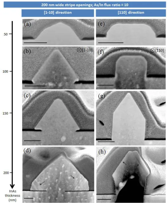
(8) Thèse de Maria Fahed, Lille 1, 2016. a) Flux calibration ...................................................................................................... 46 b) Surface reconstruction ........................................................................................... 47 1.2.2. Temperature calibration ...................................................................................... 47 2. Sample preparation ........................................................................................................... 47 2.1. Pattern elaboration ..................................................................................................... 48 2.2. Surface cleaning in MBE chamber ............................................................................ 49 3. Material characterization .................................................................................................. 52 3.1. Morphological characterization ................................................................................. 52 3.2. Structural characterization ......................................................................................... 54 3.2.1. X-Ray Diffraction: principle and experimental setup ......................................... 54 3.2.2. XRD Analysis ..................................................................................................... 55 a) Determination of epitaxial film lattice parameters ................................................ 56 b) Crystalline quality ................................................................................................. 57 Williamson-Hall model .......................................................................................... 58 Extended version of Williamson-Hall model......................................................... 59 References ............................................................................................................................ 62. CHAPTER III: Homoepitaxial selective area growth of InP and InAs ................................... 65 1. Parameters influencing the selectivity .............................................................................. 65 1.1. Growth temperature ................................................................................................... 65 1.2. V/III flux ratio ............................................................................................................ 66 2. InAs selective growth ....................................................................................................... 67 2.1. InAs nanostructure morphology ................................................................................ 67 2.1.1. As/In flux ratio influence on the nanostructure shapes ....................................... 67 2.1.2. Nanostructure shape evolution as a function of deposited thickness .................. 69 2.2. Facet growth rates ...................................................................................................... 71 2.3. InAs facet surface energies ........................................................................................ 74 2.4. Conclusion ................................................................................................................. 76 3. InP selective growth ......................................................................................................... 78 3.1. InP nanostructure morphology ................................................................................... 78 3.1.1. P/In flux ratio influence on the nanostructure shapes ......................................... 79 a) 200 nm wide stripe openings ................................................................................. 79 b) 100 nm wide stripe openings ................................................................................. 81 8 © 2016 Tous droits réservés.. lilliad.univ-lille.fr.
(9) Thèse de Maria Fahed, Lille 1, 2016. 3.1.2. Nanostructure shape evolution as a function of deposited thickness .................. 82 3.2. Facet growth rates ...................................................................................................... 84 3.3. Equilibrium Crystal Shape (ECS) model ................................................................... 85 3.3.1. InP facet surface energies .................................................................................... 85 3.3.2. Evaluation of the chemical potential from the nanostructure crystal shape ........ 86 3.3.3. Nanostructure shape evolution in the first growth stages ................................... 89 3.4. Range of values for the interface energy between InP and the mask ........................ 90 3.5. Conclusion ................................................................................................................. 93 4. General conclusion ........................................................................................................... 95 References ............................................................................................................................ 96. Chapter IV: Heteroepitaxial selective area growth of InAs/GaSb nano-heterostructures on GaAs(001) ................................................................................................................................ 97 1. Optimization of the GaSb/GaAs selective growth ........................................................... 97 1.1. Growth temperature ................................................................................................... 97 1.2. Atomic hydrogen flux during the growth ................................................................ 101 1.3. Sb/Ga flux ratio ........................................................................................................ 104 1.3.1. GaSb nanostructure morphology ....................................................................... 104 1.3.2. GaSb-lattice relaxation ...................................................................................... 107 1.4. Conclusion ............................................................................................................... 110 2. InAs/GaSb/GaAs ............................................................................................................ 110 2.1. Structural analysis .................................................................................................... 110 2.1.1. 2D growth .......................................................................................................... 110 a) STEM-analysis .................................................................................................... 111 b) XRD-analysis ...................................................................................................... 113 Williamson-Hall model ........................................................................................ 113 Extended version of Williamson-Hall model....................................................... 114 2.1.2. Selective area growth ........................................................................................ 116 a) STEM-analysis .................................................................................................... 116 b) XRD-analysis ...................................................................................................... 119 InAs on 65 nm GaSb ............................................................................................ 119 InAs on 150 nm GaSb .......................................................................................... 122 2.1.3. Discussion ......................................................................................................... 124 2.2. Chemical analysis .................................................................................................... 126 9 © 2016 Tous droits réservés.. lilliad.univ-lille.fr.
(10) Thèse de Maria Fahed, Lille 1, 2016. 3. General conclusion ......................................................................................................... 131 References .......................................................................................................................... 132. Conclusions and perspectives................................................................................................. 134. Annex: Selective area growth of GaAs/GaAs(001) ............................................................... 137. 10 © 2016 Tous droits réservés.. lilliad.univ-lille.fr.
(11) Thèse de Maria Fahed, Lille 1, 2016. 11 © 2016 Tous droits réservés.. lilliad.univ-lille.fr.
(12) Thèse de Maria Fahed, Lille 1, 2016. Introduction Over the past fifty years, the manufacturing of silicon for microelectronics has exponentially increased with strong impact in everyday life. However, during these last 10 years, the microprocessor performances face serious brakes related to the high dissipated power density and the difficulty of reducing the supply voltage without degradation in the ON current of the device [1]. This is inherent to the large effective mass of electrons and holes in Si. For this reason, the use of low effective mass materials (III-V semiconductors) in the channel for next generation of metal oxide semiconductor field effect transistor (MOSFET) is considered for increasing the transistor performance. According to ITRS 2013 roadmap, the integration of III-V semiconductors on Si will be manufactured starting in 2018 for MOSFETs [2, 3]. However, several issues such as electrostatic control, parasitic resistance and gate capacitance are still challenging to improve the device performance [4]. One possible solution to circumvent these problems is to implement 3-dimensional (3D) device architectures with low effective mass material. Some theoretical studies have shown that a trade-off can be found to find a real improvement using low effective materials as the channel of a MOSFET working at low supply voltage [1, 5]. Such architectures may take the form of the fin-shaped, TriGate, or Gate-all-around field-effect transistors [4]. Moreover, Intel recently manufactured FinFET and TriGate transistors for the 22-nm and 14-nm node CMOS technology, respectively [4, 6]. On the other hand, the integration of III-Vs on Si is also promising for the fabrication of optoelectronic components for optical interchip connections to replace metallic wires, which suffer from a too high dissipated power. Moreover, bringing together microelectronics and photonics functionalities within a unique device obviously paves the way to the fabrication of new innovative circuits. Up to now, the integration of photonic devices with Si technology has mainly relied on an hybrid scheme with III-V layers or active optical components reported on the Si platform containing all passive circuitry but a monolithic approach is highly desirable. However, the monolithic integration of III-V semiconductors on Si faces growth challenges, i.e. thermal and lattice mismatches and polarity, which affect the structural quality and hence the device operation. For both targeted applications mentioned above (3D transistors and active optical devices) and to circumvent part of the material issues, the selective area growth (SAG) of III-Vs on Si appears as an attractive approach. The growth techniques, which have been extensively used for III-V semiconductor growth, are metalorganic vapor phase epitaxy (MOVPE) and molecular beam epitaxy (MBE). For 12 © 2016 Tous droits réservés.. lilliad.univ-lille.fr.
(13) Thèse de Maria Fahed, Lille 1, 2016. planar 2D heterostructures and vertical nanowire growth, both techniques have demonstrated prominent results. However, the SAG was first developed using MOVPE since selectivity is rather easily achieved thanks to different precursor decomposition rates with respect to the substrate materials. In order to reduce the thermal budget associated with the use of high growth temperatures in MOVPE, MBE can be a valuable alternative [7]. Moreover, only few results related to the SAG of GaSb using MOVPE have been reported [8]. From this standpoint, in this thesis, we will study the SAG of III-V semiconductors on (001) substrates using MBE. As a first step and before the integration on Si, we will focus on the SAG on standard III-V substrates (GaAs and InP) and aim demonstrating GaSb SAG by MBE. This manuscript is divided in four chapters. Chapter I outlines the interest of the III-V nanostructures for microelectronics. It provides a review of the issues related to the III-V integration and processes involved in the elaboration of III-V nanostructures. The SAG background and the main targets of this PhD thesis are then exposed. Chapter II introduces the MBE growth procedure, the pattern elaboration and surface cleaning methods used in this work in a first part. The second section focuses on the morphological and structural characterization methods performed on the elaborated samples. Chapter III reports on the investigation of the homoepitaxial SAG of InP and InAs. It shows that the faceting of nanostructures selectively grown can be tailored playing with the growth conditions and the mask opening. In order to interpret these experimental results, we first determine the growth rate of each facet. If the crystal shape evolves in a more or less homothetic way (InP case), we interpret the observed shapes according to the equilibrium crystal shape model. Then using the minimization of total surface energy approach, we discuss the evolution of the nanostructure shape with the deposited thickness and we tentatively determine a range of values for the interface energy between InP and SiO2 mask. Chapter IV presents the optimization of the growth conditions for the SAG of GaSb on GaAs to promote the selectivity and growth homogeneity inside the patterns. The growth temperature, the presence of an atomic hydrogen flux during the growth and the Sb/Ga flux ratio are the growth parameters studied in this chapter. Moreover, we reveal the importance of the SAG approach on the GaSb layer quality. Finally, we demonstrate how these GaSb. 13 © 2016 Tous droits réservés.. lilliad.univ-lille.fr.
(14) Thèse de Maria Fahed, Lille 1, 2016. nanotemplates can be used as pedestals for subsequent epitaxial growth of high structural quality in-plane InAs nanowires. Finally, a conclusion and perspective part summarizes the main results obtained in this thesis and outlines the perspectives for this work in terms of device realization and growth studies.. References 1. J. A. del Alamo, Nature 479, 317, 2011. 2. www.itrs2.net 3. Viktoriia Gorbenko, “Ion beam characterisation of III-V heterostructures for micro and optoelectronic applications”, CEA-Grenoble, 2015. 4. Considerations for Ultimate CMOS Scaling, IEEE Transactions on Electron Devices 59, 7, 1813-1828. 5. K. J. Kuhn, IEEE Trans. on Electron Devices 59, 1813, 2012. 6.. M.. Bohr,. 14. nm. Process. Technology:. Opening. New. Horizons,. http://www.intel.com/content/dam/www/public/us/en/documents/pdf/foundry/mark-bohr 2014-idf-presentation.pdf 7. M. A. Wistey, et al., J. Vac. Sci. Technol. B 33, 1, 2015. 8. T. Orzali, et al., J. App. Phys. 120, 085308, 2016.. 14 © 2016 Tous droits réservés.. lilliad.univ-lille.fr.
(15) Thèse de Maria Fahed, Lille 1, 2016. CHAPTER I: III-V semiconductor selective area growth: motivation and background 1. III-V nanostructures for microelectronics 1.1. Si-MOSFET limitations and interest for III-V semiconductors In the last 50 years, Si microelectronics has known an exponential rise, which has led to many innovations in everyday life. This evolution has relied on the continuous down scaling of the metal oxide semiconductor field effect transistor (MOSFET) within the CMOS technology. However, since 15 years, this technology has entered a phase of ‘powerconstrained scaling’ [1]. Actually, the dissipated power density has reached its limit value of ≈ 100 W/cm2, which impedes further clock frequency or integration density increase without reducing the supply voltage. However, due to the large effective mass and low injection velocity of electrons and holes in Si, the reduction of the supply voltage below 0.8-0.9 V will induce degradation in the ON current of the device. One considered solution to circumvent this problem is the use of low effective mass material in the channel for next generation of transistors. The III-V semiconductor alloys InxGa1-xAs (with x ≥ 0.53) are among the best candidates for such technology due to their lower bandgap, lower electron effective mass, higher electron mobility and injection velocity, compared to Si or Ge. The introduction of such III-V materials for n-MOSFET fabrication has attracted a lot of interest in the field of microelectronics for the last fifteen years. Nevertheless, even if the use of III-Vs as channel materials in MOSFETs might allow reducing the supply voltage, the resulting performances will still be restricted by the fundamental limits of MOSFET operation, i.e. carrier thermionic emission. This leads to an upper electrostatic efficiency of the gate, defined by the subthreshlod slope (SS), which cannot reach values below 60 mV/decade. An alternative is the tunnel field effect transistor (TFET) in which carriers tunnel through the electrostatic barrier. For such transistors, III-Vs present a number of advantages due to the variety of possible heterojunctions and band alignments. Indeed, staggered or near-broken band configurations are highly desirable for the realization of TFETs with high ON current, which are encountered in the InGaAs/GaAsSb or InAs/(Al)GaSb heterostructures [2, 3]. Figure I.1 shows the lateral structures of n-type MOSFET and TFET with their corresponding energy band diagrams. In the TFET case, upon applying a positive voltage on the gate, electrons can flow from the source valence band to the channel conduction band at the source/channel tunnel junction.. 15 © 2016 Tous droits réservés.. lilliad.univ-lille.fr.
(16) Thèse de Maria Fahed, Lille 1, 2016. Figure I.1. Basic lateral MOSFET and TFET structures with the corresponding energy band diagrams.. 1.2. Challenges for III-V MOSFET integration Besides the advantages brought by III-V semiconductors, their integration in FETs based on a Si platform presents numerous challenges for both devices and materials. From a device point of view, the InGaAs alloys of interest as channel material exhibit a high electron mobility, mainly due to their low electron effective mass. This in turn reduces the 2D density of states in the channel, which limits the maximum sheet electron concentration that can be obtained and degrades the overall electrostatic control from the gate. This effect might be somewhat attenuated by the non-parabolicity of the conduction band leading to greater effective mass than predicted. On the other hand, the requirement for source and drain low resistance ohmic contacts must be fulfilled. Standard Si recipes as implantation or silicidation are less efficient with III-V materials. However, recent results have demonstrated good ohmic contacts using Ni on an InGaAs channel [4]. In the following, we discuss in more details the material issues associated with the integration of III-Vs on Si. As discussed above, the III-V materials exhibiting an appreciable interest for microelectronic applications have lattice constants close to that of InP or GaSb. However, the corresponding substrates are brittle, expensive and available in limited size. The most commercially available substrates are the Si and GaAs ones. The epitaxy of III-V materials on such substrates remains the most attractive approach in terms of integration density and cost. This approach presents challenges in terms of large lattice mismatch, difference in thermal expansion coefficients and, in the case of Si, the growth of a polar on a non-polar material. For these reasons, III-V materials grown on Si generally exhibit a large density of defects. 16 © 2016 Tous droits réservés.. lilliad.univ-lille.fr.
(17) Thèse de Maria Fahed, Lille 1, 2016. such as threading dislocations (TDs), inversion domain boundaries called antiphase boundaries (APBs), micro-twins or cracks. 1.2.1. Lattice mismatch Before beginning this section, it is mandatory to present the Si and III-V compound crystal structures. III-V compound semiconductors have a zinc-blende structure, where group III atoms occupy the positions of a face-centered cubic unit cell and group V atoms occupy the positions of a second face-centered unit cell shifted by (a/4, a/4, a/4) with respect to the first one (figure I.2(b)).. Figure I.2. Unit cell structure of a diamond lattice (a) and zinc blende lattice (b) [5].. Each atom is bonded to the four neighboring atoms of the other group. On the other hand, Si has a diamond cubic crystal structure (figure I.2(a)). The lattice mismatch between the epilayer and the substrate as a function of the lattice constants of the epilayer (alayer) and the substrate (asubstrate) is given by: 𝑓=. 𝑎𝑙𝑎𝑦𝑒𝑟 −𝑎𝑠𝑢𝑏𝑠𝑡𝑟𝑎𝑡𝑒. (Eq.I.1). 𝑎𝑠𝑢𝑏𝑠𝑡𝑟𝑎𝑡𝑒. When f < 2 %, the growth begins according to the Frank-van der Merwe (layer-by-layer or 2D) growth mode [6]. The in-plane lattice constant of the epilayer is imposed by the substrate and the epilayer experiments a bi-axial stress. This latter gives rise to an elastic energy increasing with the layer thickness. Once the critical thickness hc is reached, the elastic energy is partially released by the introduction of misfit dislocations (MDs). Many studies have been devoted to the determination of hc during 2D growths [7]. When 2 % < f < 6 %, the growth follows a Stranski-Krastanov growth mode (combined layer-by-layer + island growth) [6]. Here, a 2D layer precedes a transition towards 3D growth leading to the formation of strained islands on the top surface. The critical thickness is defined. 17 © 2016 Tous droits réservés.. lilliad.univ-lille.fr.
(18) Thèse de Maria Fahed, Lille 1, 2016. at the onset of this transition. Upon further growth, islands become bigger with the introduction of MDs before coalescence inducing even more defects. When f > 6 %, small islands are nucleated directly on the substrate: this is called VolmerWeber (3D) growth mode [6]. In this case, the critical thickness is reached immediately when the growth begins (hc ≈ 1 ML). After island coalescence, the TD density is very high. Therefore, there is strong link between the mismatch and the dislocation density. In a general way, a dislocation can be understood as a combination of the two basic ones: the edge and screw dislocations. The edge dislocation introduces a half extra plane into a crystal, as it is shown in figure I.3(a). The dislocation line is the line where the half-plane terminates and it is perpendicular to the Burgers vector. This latter may be determined by consideration of a closed loop (atom to atom path) around the dislocation core.. Figure I.3. Schematic diagrams of edge (a) and screw (b) dislocation in a cubic lattice. The dislocation line ξ and Burgers vectors b (red arrows) are shown [8].. On the other hand, the screw dislocation shears one part of the crystal with respect to the other one within a half-plane (figure I.3(b)). In this case the dislocation line corresponds to the position where the half-plane terminates and is parallel to the Burgers vector [9-10]. A mixed dislocation type is defined as resulting from a mixture of edge and screw dislocations with the dislocation line making an angle in the 0°-90° range with the Burgers vector. The two most commonly observed dislocations in highly mismatched III-V (001) growth, are the 60° and 90° ones, the latter being called Lomer dislocations. The 60° dislocation is a mixed type dislocation, with edge and screw components. In addition, the interaction of two 60° dislocations might lead to a 90° dislocation. 18 © 2016 Tous droits réservés.. lilliad.univ-lille.fr.
(19) Thèse de Maria Fahed, Lille 1, 2016. For low mismatch values, plastic relaxation occurs mainly via the introduction of 60° dislocations. Dislocation loops nucleate from the surface and propagate through the epilayer until the misfit segment reaches the interface and results in two threading segments [11]. Figure I.4(a) shows the TD and MD propagation inside the mismatched layer in one crystallographic direction. We notice an elongation of the MD at the interface and an elimination of the TD. However, if the same procedure occurs in two crystallographic directions, as it is shown in figure I.4(b), a TD will degrade the epitaxial layer due to the interaction of the TD and MD gliding in two different (111) planes.. Figure I.4. Schematic of TD and MD propagation inside a mismatched layer in one (a) and two (b) crystallographic directions [12].. For high mismatch, 90° dislocations are progressively introduced at the edges of growing islands and are directly located at the substrate epilayer interface [13, 14]. However, even in this case, upon island coalescence, 60° dislocations can be introduced from the surface. The TDs form non-radiative recombination centers and accelerate the impurities diffusion along their lines. For this reason they are known as a cause of damage for device performance and reliability [15]. 1.2.2. Antiphase boundaries (APBs) Basically, APBs are two-dimensional arrays of atomic bonds between III-III or V-V atoms in a III-V material. The generation of APBs has been largely investigated in epitaxial growth of III-V materials on Si(001) [16-17]. As there is a difference in the crystal structure of group IV (Si) and III-V materials, APBs can arise during the epitaxial growth of III-V semiconductors on Si [18]. An APB might be generated at the coalescence region of two III-V material domains that have nucleated with different starting atoms (group III or V atoms) on a (001) surface of an elemental semiconductor (Si). However, in most cases, since III-V growth 19 © 2016 Tous droits réservés.. lilliad.univ-lille.fr.
(20) Thèse de Maria Fahed, Lille 1, 2016. is initiated by either a group-III or a group-V supply, APBs will arise from III-V domains nucleated on two different Si terraces separated by a monoatomic step as it is shown in figure I.5(a). Since the APBs contain III-III or V-V atomic bonding in a matrix of III-V bonds, as in the case of dislocations, the APBs degrade the device performance significantly. Therefore, it is essential to eliminate the APBs for the integration of highly performing III-V materials on Si.. Figure I.5. Growth of GaAs on a Si(001) surface having monoatomic steps: presence of APBs (a), and double steps: no APBs (b)[19].. 1.2.3. Thermal expansion Besides the effects discussed above, the difference in thermal expansion coefficient between the layer and the substrate also plays a role in degrading the layer quality. Table I.1 presents the lattice parameters and the thermal expansion coefficients for Si and the III-V compounds at 300 K [19]. Therefore, if the lattices match at the growth temperature (in most cases > 500°C), upon cooling, the thermal expansion coefficient difference generates a stress in the epilayer which can lead to deformation or even to the appearance of cracks. For a given substrate/epilayer system, this difference in thermal expansion coefficients fixes an upper limit of the thickness that can be grown without crack formation.. 20 © 2016 Tous droits réservés.. lilliad.univ-lille.fr.
(21) Thèse de Maria Fahed, Lille 1, 2016. Table I.1 Lattice constant and thermal expansion of III-V and Si materials at 300K [19].. Lattice constant (Å) GaSb GaAs Si InAs InP InSb AlSb. 6.0959 5.6533 5.431 6.0584 5.8687 6.4794 6.1355. Thermal expansion coefficient (10-6 /K) 6.35 6.03 2.616 4.28 4.6 5.04 4.2. 1.2.4. Conclusion A lot of work has been done in the past to answer these issues, keeping the planar geometry. More recent works tend to prove that the most efficient solutions could be demonstrated using 3D nanostructures. These nanostructures may be efficient to solve some material issues (TD density, thermal expansion difference) but also to address the drawback of III-V materials. Indeed, 3D nanostructures can provide a solution for improving gate electrostatics (Ω-gate or gate all around transistors) or ohmic contacts (raised heavily doped source-drain contacts). In the following, we highlight the main results demonstrating the benefit of III-V nanostructures for microelectronic applications. 1.3. III-V nanostructures For nanostructure-based devices, two main fabrication schemes are considered: the top-down and the bottom-up processes. The first one consists in growing first a 2D material before the definition of nanostructures by means of lithography and etching techniques. The latter includes two approaches: the nanowire growth with or without metal catalyst particles or selective area growth (SAG) on a (111) substrate and the SAG on a (001) substrate. 1.3.1. Top-down process a) Nanowire based devices Many attempts have been reported on MOSFET and TFET fabrication using III-V materials. For example in a recent work, Gu et al. have presented a comparison between planar and 3D MOSFETs based on InGaAs/InP at deep sub-micron gate lengths [20]. They claim that the 3D configuration greatly improves the off-state performance and facilitates enhancement-mode operation. Regarding TFETs based on InGaAs/InP, Rajamohanan et al. have demonstrated an improvement in electrical quality (low OFF state current) by achieving 21 © 2016 Tous droits réservés.. lilliad.univ-lille.fr.
(22) Thèse de Maria Fahed, Lille 1, 2016. a channel etching method which decreases the damage in the mesa sidewall [2]. Moreover the work of Zhao et al. reveals InGaAs/InAs TFETs having a diameter of 15 nm, using a novel III-V dry etching process and gate-source isolation method. The nanowire TFET schematic and SEM image are represented in figure I.6 [21]. They demonstrate an excellent combination of steep slope (79 mV/dec) and ON current compared to other nanowire TFETs with III-V materials.. Figure I.6. Nanowires TFETs schematic and design parameters. SEM image of InGaAs nanowire TFET of diameter 15 nm defined by dry etching technique. [21].. While this approach has enabled an important number of device demonstrations, it reveals also several difficulties. On one hand, the etching process can induce damages on the semiconductor surface. On the other hand, the approach of starting from a 2D heterostructure leads to an important defect density when GaAs or Si substrates are used [1]. Since these defects can degrade the device performances, many attempts have been tried to mitigate the detrimental defects. In the next part, we present the main methods that were developed in 2D growth to impede the mismatch issues on the III-V layer grown on Si and GaAs substrates. b) Towards defect reduction Threading dislocation density (TDD) Many researchers have claimed an optimization of the mismatch strain accommodation in the case of highly lattice-mismatched materials using a gradual metamorphic approach (compositionally graded-layers) [22-23]. The goal is to slowly increase the strain during the buffer growth so that dislocations are introduced progressively, avoiding the blocking process described in figure I.4(b) and hence the formation of TDs. It has demonstrated a number of perfectly relaxed heterostructures, with the further successful fabrication of devices [24-26]. However, this requires the growth of thick buffer layers (> 1 µm) [27], leading to poor 22 © 2016 Tous droits réservés.. lilliad.univ-lille.fr.
(23) Thèse de Maria Fahed, Lille 1, 2016. thermal and electrical conductivities and therefore making this method not very satisfying for devices. In order to reduce the TDD, another way is to promote the formation of an interfacial 90° misfit dislocation array (IMF). This approach consists in creating a network of 90° (edge) MDs at the layer/substrate interface which relaxes most of the strain coming from the mismatch at the interface in both [110] and [1-10] directions and leads to a strain free layerby-layer growth [28]. Almost strain-free layers grown via IMF have been demonstrated for several systems such as InAs/Ga(As, P) [29-31] and GaSb/GaAs [32]. Moreover, in the case of GaSb growth on Si or GaAs, the role of an AlSb interlayer has been extensively investigated [33-36]. However, the growth mechanism remains still unclear and the resulting TDD for µm-thick overlayers is rarely below 108/cm2. Antiphase boundaries (APBs) The key point to eliminate APBs in heteroepitaxy of a polar semiconductor on Si(001) is the elimination of monoatomic surface steps [37]. The overgrowth on double steps is free from APBs, as shown in figure I.5(b). If the Si (001) substrates are offcut by > 4° toward a [110] direction and are annealed, only double steps exist on the surface [38-40]. The APBs can be annihilated by the use of such surfaces, during the growth of III-V compounds [41-44], as for instance GaAs, GaSb [42-45], GaP [46-49], as well as AlSb [50]. However, these miscut substrates are not suitable for device processing. Indeed, all device areas should be exactly oriented with respect to the miscut direction to obtain double steps all over the surface, which is not obvious [51]. Nevertheless, recent results from Bogumilowicz et al have demonstrated the growth of APB-free GaAs epilayers on quasi nominal (001) Si, with a miscut angle <0.5° along the [110] direction [52]. In the same vein, Volz et al. concentrate on APB-free nucleation of GaP on exact Si(001) substrates [53]. 1.3.2. Bottom-up process Besides the top-down approach, an efficient method for reducing the defect density is the bottom-up process [54-55]. The nanowire growth approach in order to fabricate devices is a very attractive idea because it allows attaining narrow channels defined by the nanowire diameter in the 10-50 nm range, hence promoting electrostatic control. Li et al. have grown InAs nanowires on a Si(111) substrate by molecular beam epitaxy (MBE). In this work, a nanowire with a 20 nm diameter is selected and transferred for horizontal device fabrication [56]. Burke et al. followed a similar approach to make horizontal wrapped-gate nanowire 23 © 2016 Tous droits réservés.. lilliad.univ-lille.fr.
(24) Thèse de Maria Fahed, Lille 1, 2016. transistors [57]. With the aim to impose the nanowire position and area, the SAG was used on (111) substrates. For instance Tomioka et al. have reported a device based on InAs nanowires grown using the SAG approach on Ge(111) substrate by metalorganic vapor phase epitaxy (MOVPE) [58]. They demonstrate a high-performance of vertical InAs nanowire surroundinggate transistor. The growth of nanowires on (111) surfaces leads to nanostructures free from APB. However, the use of these vertical nanowires grown on (111) substrates for device fabrication suffers from two main issues. The first one is related to the important density of crystalline defects along the nanowire, mainly stacking faults (SFs), twins and polytypism for which the zinc blende and wurtzite phases coexist within the same nanowire (figure I.7). The stacking sequence of the zinc blende structure along the [111] direction can be written as ʺABCABCʺ. When a SF occurs, either it gives rise to an extra atomic plane ʺABCBABCʺ or it removes one ʺABCBCʺ. Another type of defect is the twin, which occurs exclusively on (111) planes with the following stacking sequence ʺABCABACBAʺ. These crystalline defects degrade the electronic transport properties as shown in the case of InAs nanowires [59]. The second drawback of these vertical nanowires concerns the device processing involving 3 vertically stacked contacts (source, gate and drain). Finally, the standard substrate orientation for microelectronic applications is the (001) one and not the (111) one.. Figure I.7. TEM images illustrating InAs nanowires grown by MOVPE, exhibiting SFs, twins and polytypism for which the zinc blende and wurtzite phases coexist within the same nanowire [59].. This appeals for the growth of in-plane nanowires on (001) substrates. Using such approach, Borg et al. have demonstrated an InAs-Si heterojunction nanowire tunnel diode grown inside a horizontal SiO2 nanotube template fabricated on a Si(001) substrate. They show that this process permits to obtain nanowires free from dislocations, and with an orientation and dimension directly given by the shape of the template [60]. SAG has also been applied to raise 24 © 2016 Tous droits réservés.. lilliad.univ-lille.fr.
(25) Thèse de Maria Fahed, Lille 1, 2016. source/drain ohmic contacts, highlighting the control and design of the regrown areas by changing the growth parameters [61]. 1.4 Conclusion In this section we have shown that the integration of low effective mass III-V materials on standard semiconductor substrates using 2D growth faces difficulties, which increase the defect density inside the grown layer and degrade the device characteristics and reliability. The first one comes from the mismatch between the epilayer and the substrate, the second one arises from the difference in thermal expansion coefficients, and the third one is the APBs present in the case of III-V growth on Si. For the APB problem, more or less feasible solutions can be implemented. However, the first two problems are difficult to manage. For instance, in the case of GaSb grown on GaAs, the 7.8% mismatch leads to a threading defect density in the 108 cm-2 range [62]. In order to overcome these problems, the nanowire growth approach has been considered. Many attempts have been reported on the elaboration of vertical nanowires and associated devices. However, this fabrication route suffers from degraded crystalline quality and is not convenient for technological processing due to the use of a (111) substrate orientation. Therefore, our goal is to elaborate high quality in-plane III-V nanostructures on (001)oriented substrate. The previous studies based on this approach will be discussed in the next section.. 2. Selective area growth background Since our goal is to study the SAG of III-V materials, in this part we discuss the previously achieved work in this framework. Firstly, we present the experimental results then we turn to the discussion of the models for crystal shape interpretation. 2.1. Experimental results In this section, we review the previous work done on the SAG of III-V semiconductors. Firstly, we highlight the growth conditions leading to the selectivity with respect to an oxide mask i.e. with no polycrystal deposition on the oxide mask. Then, we focus on the III-V semiconductor shape inside openings. In this context two systems will be discussed: the homoepitaxial and the heteroepitaxial ones. 2.1.1. Selectivity Several experiments have been dedicated to the growth on a semiconductor substrate covered by a dielectric mask (in most cases SiO2) in which openings have been defined by 25 © 2016 Tous droits réservés.. lilliad.univ-lille.fr.
(26) Thèse de Maria Fahed, Lille 1, 2016. lithography. The selectivity conditions depend on the epitaxy techniques. For the growth techniques based on metalorganic compounds (TMGa, TMAl, …), such as metalorganic vapor phase epitaxy (MOVPE) or metalorganic molecular beam epitaxy (MOMBE), III-V material grows inside windows opened in the oxide, but there is no deposition on the oxide itself. This is due to the fact that the mask does not catalyze the decomposition of the metalorganics. Therefore, the condition for SAG using metalorganic-based techniques relies mostly on the mask type and weakly on the growth conditions (temperature, growth rate, III/V flux ratio…), i.e. the SAG conditions can be rather similar than those used for conventional (non-selective) growth [63]. However, for techniques such as MBE (having elemental sources), which do not rely on the catalyzed surface decomposition of molecules, the realization of the SAG is not achievable without modifying the growth conditions. Indeed, for this growth technique the selectivity mechanism is only related to the re-evaporation and diffusion of group-III elements deposited on the mask. This mechanism can be achieved using a low growth rate or/and a high growth temperature. Figure I.8 shows an example of GaAs nucleation on a SiO2 mask using a fixed Ga flux ratio of 0.1 ML/s and by varying the growth temperature (GT) from 630 to 585 °C [64]. In order to optimize the selectivity, the GT must be higher than 630°C. Another attempt was claimed on the SAG of InxGa1-xAs, where the selectivity was demonstrated at a GT of 595°C [65]. In both cases, the GT must be high and the growth rate low enough to allow selective growth.. Figure I.8. SEM images of 100 nm of GaAs grown on un-patterned SiO2 surfaces when varying the growth temperature from 630 to 585 °C. The Ga flux ratio is 0.1 ML/s. [64]. 26 © 2016 Tous droits réservés.. lilliad.univ-lille.fr.
(27) Thèse de Maria Fahed, Lille 1, 2016. In MBE, the selectivity will mostly depend on the difference of sticking and diffusion coefficients of the group-III element on the mask and semiconductor surfaces respectively [66]. For GaAs, the above example shows that selectivity can be achieved reducing the growth rate and choosing the high limit of GT with respect to 2D growth conditions. In other words, it means that there exists a growth condition for which good quality GaAs can be grown in the openings without any polycrystalline material nucleation on the mask. Turning now to GaSb SAG, considering that the group-III element is still Ga, similar growth conditions as for GaAs should be used. However, good quality GaSb layers are usually obtained at a much lower GT, around 500°C [67-68]. A reduction of the GT is therefore very important to obtain high quality epitaxial nanostructures. One way to improve the growth selectivity for some III-V materials at low temperature with respect to a SiO2 or a Si3N4 mask is the addition of an atomic hydrogen flux during the epitaxy as it has been demonstrated in the case of GaAs, GaInAs or InP [69-70]. Sugaya et al. have proposed a mechanism based on the enhanced Ga and As desorption from the SiO2 surface due to the formation of Ga and As hydrides [69]. In the same way, Kuroda et al. have shown that the dominant factor of the selective growth mechanism of InGaAs/InP under H atomic flux is not an enhanced In and Ga atom migration from the masked regions to the growing regions, but rather an increased In and Ga atom desorption from the mask surface [70]. Actually, they claimed that the presence of the atomic hydrogen leads to the formation of Ga and In hydrides since the bond strength of Ga-H (66 kcal/mol) and In-H (58.1 kcal/mol) is larger than that of Ga-As (50 kcal/mol), In-As (48 kcal/mol), and In-P (47 kcal/mol) [71]. Therefore, on the mask surface, the Ga and In atoms tend to bind with atomic hydrogen rather than with As and P atoms, impeding the formation of polycrystalline InGaAs on the mask surface. This in turn may imply that for atomic hydrogen assisted growth of InGaAs on an unpatterned InP surface, hydride formation should occur and result in a lower thickness than the nominal one. Indeed, Kobayashi et al. have reported that atomic hydrogen reacts with Ga atoms and removes them from the GaAs surface annealed at a temperature higher than 850°C [72]. However, Bachrach et al. have claimed that the interaction between atomic hydrogen and (001) GaAs surfaces which leads to the formation of Ga hydrides is restricted to the top surface layer and cannot be ascribed to an etching mechanism [73]. To our knowledge, up to now, no results on the SAG of GaSb by MBE have been reported.. 27 © 2016 Tous droits réservés.. lilliad.univ-lille.fr.
(28) Thèse de Maria Fahed, Lille 1, 2016. 2.1.2. Crystal shape The growth conditions, lattice mismatch and the opening size are the main parameters that may affect the crystal shape inside the opening windows. Actually, the control of the IIIV arrangement inside the openings is very important since it is related to the device efficiency. In this section, we present previous work done on the homoepitaxial and the heteroepitaxial SAG in order to control the crystal shape inside the openings. For each SAG type, we first present the attempts demonstrated on micrometer scale patterns and we then focus on the ones at nanometer scale due to the continuous development of nanoscale lithography techniques. a) Homoepitaxial SAG The studies on the homoepitaxial SAG were the first step to understand the SAG mechanism. Firstly, it has been devoted to micrometer scale patterns, as for instance in the work of Bauhuis et al. which details the faceting of GaAs microcrystals grown by MOCVD inside square openings having an edge size going from 5 to 20 µm. They claimed that the final shape does not depend on the opening size, due to the constant growth rate of the facets [74]. Later on, Ujihara et al. studied the effect of the spacing between stripes, varying it from 1 to 20 µm for a fix opening size of 240 nm, on the InP crystal shape [75]. They compared their experimental findings with a model taking into account the surface and vapor phase diffusion [76]. When the spacing between patterns is comparable to the surface diffusion length on the mask, the surface diffusion contribution is dominant, and the surface diffusion length was estimated to be around 1-2 µm. Let us now turn the discussion to the SAG inside nanostructured patterns. At this length scale mastering the nanocrystal shape is of paramount importance since it affects the optoelectronic and microelectronic states inside the semiconductor nanostructures such as quantum dots or nanowires. A recent work reports the influence of the base size and shape on the formation of InP pyramids by SAG using MOVPE, stressing the interplay between the major low-index facets in the final shape [77]. The aim of such study is to control the position and distribution of InAs quantum dots grown on these designed InP pyramids [78]. For the same goal, but using a vicinal GaAs surface, Fukui et al. have shown that when the misorientation angle of the substrate increases, the surface migration of Ga adatoms from the sidewall facets to the top region decreases, due to high step density enhancing the growth rate on the sidewalls [79].. 28 © 2016 Tous droits réservés.. lilliad.univ-lille.fr.
(29) Thèse de Maria Fahed, Lille 1, 2016. Recently Lee et al. have explained the faceting of GaAs nanostructures directed along [110] in the framework of the equilibrium crystal shape model (ECS) [80-81], using the relative surface energy of the involved facets [82-84]. In this approach, the evolution of the facets is predicted according to the equilibrium theory and Wulff geometrical construction [81]. In the same way, the formation of vertical facets in one-dimensional high-aspect ratio GaAs gratings has been interpreted based on the minimization of total surface energy [84]. b) Heteroepitaxial SAG In the goal of accommodating lattice mismatched heterostructures using SAG approach, the crystal shape behaviors were also studied. In the 90’s, the heteroepitaxial SAG of unstrained heterostructures has been studied on micrometer scale patterns, as for instance in the work of Heinecke et al. which details the faceting of InP microcrystals grown on GaInAs depending on the opening orientation and the value of the P/In ratio using MOVPE or MOMBE. They achieved vertical sidewalls on the grown structures for high P/In ratios using small substrate misorientation [85-87]. These investigations can be used for the integration of optical devices. For the same III-V system, Kayser et al. studied the effect of the PH3 flux on the crystal shape using MOMBE inside 10 µm opening size [88]. When the PH3 flux increases, the migration length from the (111)B facets to (001) ones decreases and the crystal shape exhibits an “ear” formation, as it is represented in figure I.9. In contrast, for a low PH3 flux, a uniform transfer of material from (111)B facets to (001) ones is observed, i.e. the migration length from the (111)B facets to (001) ones increases.. Figure I.9. Schematic of the surface migration processes on (111)B and (001) surfaces as a function of PH3 flux [85].. More recently and for nanostructured patterns, Wang et al. have successfully used the SAG technique inside SiO2 nano-trenches on Si to grow InP-based lasers on Si (001) [89]. They showed that this novel epitaxial technology suppresses threading dislocations and anti-phase boundaries for a deposited thickness as low as 20 nm. In the same way, Cipro et al. have 29 © 2016 Tous droits réservés.. lilliad.univ-lille.fr.
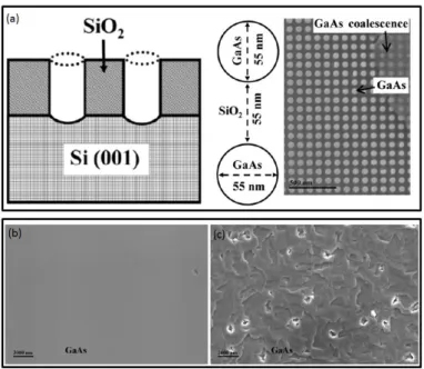
(30) Thèse de Maria Fahed, Lille 1, 2016. shown that growing directly GaAs in SiO2 cavities patterned on a nominal Si(001) surface is efficient to completely annihilate the APBs [90], thanks to the aspect ratio trapping (ART) mechanism [91]. Figure I.10 shows an example of GaAs grown on Si(001) using the ART approach. Via an aspect ratio (trench height/ trench width) of 1.8, the dislocations originating at the GaAs/Si interface are trapped by the oxide sidewalls leading to defect-free GaAs at the top of the trenches. In the same vein, Paladugu et al. demonstrate the minimization of the APBs by performing the selective epitaxial growth of III-V material on Si inside “V-grooves” with (111) facets [92].. Figure I.10. Cross-sectional TEM images of GaAs on Si(001) in SiO2 patterned trenches of aspect ratio of 1.8. Some defects are caused by coalescence: D indicate dislocations; P indicate planar defects [91].. Another approach based on SAG was investigated by Renard et al. in order to avoid the emission of MDs and the formation of APBs. This procedure consists in the lateral overgrowth after nucleation in 50 nm wide openings [93-94]. Using this approach, Yi et al. have reported the lateral overgrowth of GaSb nanostructures on the oxide mask using MOCVD. They showed that the GaSb films exhibit defects when the GaSb nanostructures coalesce [95]. Regarding the SAG of GaAs on Si (001), Hsu et al. have investigated the MOCVD growth on a 55 nm round-hole patterned SiO2 mask on a Si substrate (figure I.11(a)). They showed that due to the blocking of the TDs along the SiO2 walls, a reduction of the number of dislocations can be observed [96], as highlighted in the SEM images of the growth on a patterned (figure I.11(b)) and non-patterned substrate (figure I.11(c)). Moreover, Suryanarayanan et al. achieved a reduction of the defect density in an InAs epilayer grown on GaAs(001) using lateral epitaxial overgrowth by MOCVD [97]. They demonstrated that when 30 © 2016 Tous droits réservés.. lilliad.univ-lille.fr.
(31) Thèse de Maria Fahed, Lille 1, 2016. the opening width is less than 1 µm, the InAs-microstructure shape changes in a way that accelerates defect reduction.. Figure I.11. Schematic diagrams showing the nanopatterned Si(001) substrate and the round-hole diameter and spacing, SEM image of the first step of GaAs filling the round holes (a), SEM images of 900 nm-thick GaAs deposited on patterned substrate (b), and non-patterned one (c) [97].. 2.2. SAG modeling Whatever the length scale considered, the final crystal shape is determined by: . Surface/interface energies [98]. . Facet kinetics [99-101]. 2.2.1. Equilibrium crystal shape (ECS) When growth is not kinetically limited, the nanostructure shape can be interpreted considering previously calculated surface energies of the involved facets, which leads to the ECS model [98], [102]. To do that, the Wulff geometric construction on the observed 2D nanostructures is often used [103]. Different cases have to be considered: . The growth is stress free, when the substrate and film have the same lattice constant (f = 0).. . The growth is pseudomorphic, when the film is stretched (f < 0) or compressed (f > 0) such that the substrate and the film in-plane lattice constants coincide.. In the following, we discuss the ECS model as a function of the mismatch between the layer and the substrate [104].. 31 © 2016 Tous droits réservés.. lilliad.univ-lille.fr.
(32) Thèse de Maria Fahed, Lille 1, 2016. When f = 0, two cases are considered: in the first one, the substrate and layer materials are similar (free crystal) whereas in the second case they are different with the same lattice constant (unstrained crystal). For an isolated crystal, the equilibrium shape is found by minimizing, at constant volume, the Gibbs surface free energy (G) given by [104]: 𝐺 = ∑𝑖 𝜎𝑖 . 𝐴𝑖. (Eq.I.2). where Ai and σi are the area and the surface energy of the facet i of the crystal, respectively. The equilibrium shape can be found with a geometrical construction based on the Wulff theorem: 𝜎𝑖 𝐻𝑖. = 𝐶𝑜𝑛𝑠𝑡𝑎𝑛𝑡. (Eq.I.3). where Hi is the distance of each facet (i) from a common point (Wulff’s point) inside the crystal (figure I.12(a)). Therefore, for a free crystal growing in equilibrium conditions, its shape for different sizes (different constant) is similar around the common Wulff’s point. Considering now the growth of a crystal “A” on a substrate “B”, the equilibrium shape in the absence of misfit can be again determined only by the minimization of the surface and interface energies. Besides the crystal “A” free facets of area Si, the contact area AAB with the substrate “B” must be introduced in such a way that the Gibbs surface free energy (G) is as following [104]: 𝐺 = ∑𝑖 𝜎𝑖 . 𝐴𝑖 + 𝐴𝐴𝐵 (𝜎𝐴𝐵 − 𝜎𝐵 ). (Eq.I.4). Figure I.12. Equilibrium shape evolution of a free crystal (a); of an island A on a substrate B having the same lattice parameter (b) [104].. 32 © 2016 Tous droits réservés.. lilliad.univ-lille.fr.
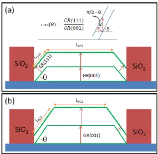
(33) Thèse de Maria Fahed, Lille 1, 2016. The interfacial energy σAB is defined as a function of the adhesion energy of A on B (β): 𝜎𝐴𝐵 = 𝜎𝐴 + 𝜎𝐵 − 𝛽. (Eq. I. 5). From Wulff-Kaichew theorem we get: 𝜎𝑖 𝐻𝑖. =. 2𝜎𝐴𝐵 −𝜎𝐵 𝐻. = 𝐶𝑜𝑛𝑠𝑡𝑎𝑛𝑡. (Eq.I.6). where H is the emerging height of the crystal (figure I.12(b)). In this case (absence of misfit), the equilibrium shape maintains self-similarity above the substrate surface. When f ≠ 0, an epitaxially strained crystal A is deposited on a lattice mismatched (f) substrate B. The equilibrium shape determination in this case is more complicated. Using the WulffKaichew theorem, Muller et al. have studied the ECS of a 3D crystal deposited onto a latticemismatched substrate [104]. Jiang et al. reported a particular case of SAG of mismatched III-V materials on Si inside deep submicron trenches where they assume that the defect density is reasonably low [101]. Neglecting the effect of defects and using surface energy minimization, they determine the ratio between the facet lengths when the crystal is in an equilibrium state. This approach gives the same result as using the Wulff plot (discussed above) and simple geometrical arguments. They found that for the same growth conditions and when the growth proceeds, the following equation should be satisfied [101]: 𝐿001 𝐿111. = 𝐶𝑜𝑛𝑠𝑡𝑎𝑛𝑡. (Eq.I.7). where L001 and L111 are the lengths of (001) and (111) facets, respectively (figure I.13(a)).. Figure I.13. Schematic of the equilibrium (a) and non-equilibrium (b) shape evolution inside submicron trenches.. 33 © 2016 Tous droits réservés.. lilliad.univ-lille.fr.
(34) Thèse de Maria Fahed, Lille 1, 2016. To follow the evolution of the crystal shape during growth, growth rates (GR) for (001) and (111) facets can be measured [105-106]. Using simple geometrical arguments shown in the inset of figure I.13(a), to keep constant the facet length ratio in Eq. I.7, the GR(001) and GR(111) must obey to : 𝐺𝑅(111) 𝐺𝑅(001). = cos(𝜃). (Eq.I.8). If Eq. I.7 is not satisfied, one of the two facets ((001) or (111)) will disappear (figure I.13(b)). This is illustrated for instance in the work of Dutartre et al. where the facet GRs of Si inside 1 µm wide trenches are determined using SiGe layers as markers [107-109]. They demonstrated that the facet GRs do not change when the growth proceeds inside the trenches (figure I.14). However, Eq. I.8 and I.7 applied to (001) and (113) facets are not satisfied during the growth, which therefore does not proceed under equilibrium conditions. This in turn implies that facet kinetics must be considered.. Figure I.14. SEM image recorded for the SAG of Si using a layer of SiGe as a marker [107].. 2.2.2. Facet kinetics Facet kinetics includes the surface diffusion (SD) on the facets and the surface attachment/detachment processes [110]. When discussing the SD mechanism on patterned substrates, it is assumed that the adatoms can be easily attached to/detached from the lattice when the growth proceeds. Conversely, in the case of surface attachment/detachment limiting case, the effect of SD can be neglected, i.e. a fast transport through a surrounding surface layer is assumed. However, in practice, it is not obvious to separate the SD and the surface attachment/detachment processes and most experimental works have been devoted to surface diffusion effects.. 34 © 2016 Tous droits réservés.. lilliad.univ-lille.fr.
(35) Thèse de Maria Fahed, Lille 1, 2016. Indeed, the SD process was firstly extensively studied on 2D growths in order to measure the SD length of the group-III element atoms. In the 1990s, Hata et al. and Shen et al. have evidenced the surface diffusion length of Ga atoms during MBE growth of GaAs by means of reflection high-energy electron diffraction (RHEED) intensity oscillations [110-113]. These studies show that Ga atoms are quite mobile on the growing surface. The Ga surface diffusion length reaches as far as several micrometers and increases with decreasing V/III ratio [114]. In the same vein, Ohtsuka et al have reported another important result demonstrating that the Ga diffusion length significantly depends on the surface orientation [115]. Using a numerical simulation, they found the variation of the Ga diffusion length as a function of the surface orientation in the case of GaAs growth by MBE. These results are presented in figure I.15, where we notice that the minimum value of the Ga diffusion length is about 0.5 µm. These findings are further confirmed by the works of Ujihara et al. and Shen et al. who have reported typical values for the diffusion length of group-III element in the µm-range on patterned InP and GaAs substrates using MOVPE and MBE [116-117]. Therefore, the effect of the SD depends of the pattern dimensions. If this latter is below the typical SD length of the impinging species at the surface, then the effect of surface diffusion kinetics will be reduced.. Figure I.15. Diffusion length versus surface orientation angle [115].. Jiang et al., have modeled the effect of kinetics on the evolution of (001) and (111) facets for the crystal shape inside submicron trenches [101]. The two possible migration directions towards the equilibrium shape are schematically shown in figure I.16. The first migration direction consists of an inter-facet surface migration from facet (111) to facet (001), and the opposite for the second migration direction (from (001) to (111)). 35 © 2016 Tous droits réservés.. lilliad.univ-lille.fr.
(36) Thèse de Maria Fahed, Lille 1, 2016. Figure I.16. Schematic of III-V SAG inside submicron trenches on (001) Si substrates and the two possible migration direction before reaching the equilibrium shape [101].. 3. Thesis objectives We have shown the importance of growing III-V semiconductor nanostructures on GaAs and Si substrates for microelectronic applications. We have then exposed the main problems related to the integration of III-V materials on GaAs and Si substrates such as thermal expansion coefficient, polarity or lattice constants. On the other hand, the useful active area of semiconductor being in most cases reduced to a few tenths of nanometers square per device, thanks to nanoscale lithography techniques, we have focused on the SAG approach using (001) substrates which allows the control of the nanostructure position. In order to overcome these problems, the growth of vertical nanowires has been extensively developed in the last 15 years. However, besides crystal phase polymorphism issues, the inconvenience of this method is the use of a (111) substrate orientation. Therefore, our goal is to elaborate high quality in-plane III-V nanowires, using (001) substrate orientation. We will first try to understand the mechanisms driving III-V nanocrystal shape inside oxide openings, in the framework of the ECS model and the kinetics phenomena described above. To do this, we will start with the simple case of III-V homoepitaxy (no strain), considering the. 36 © 2016 Tous droits réservés.. lilliad.univ-lille.fr.
(37) Thèse de Maria Fahed, Lille 1, 2016. InP and InAs cases. We will particularly show how the growth conditions can be used to tailor the nanocrystal shape. Then, using the SAG approach we will try to achieve, high quality GaSb and InAs nanowires grown on highly mismatched GaAs (001) substrate. We will first show the influence of the growth conditions on GaSb nanowire growth inside stripes directed along [110] and [1-10]. After the optimization of GaSb growth conditions, we will grow 10-nm thick InAs on top of these GaSb nanotemplates to achieve in-plane InAs nanowires. After GaSb selective etching in an ammonia-based solution, free standing InAs nanowires will be established.. 37 © 2016 Tous droits réservés.. lilliad.univ-lille.fr.
Figure

![Figure I.14. SEM image recorded for the SAG of Si using a layer of SiGe as a marker [107]](https://thumb-eu.123doks.com/thumbv2/123doknet/3716300.110860/34.892.261.635.535.797/figure-sem-image-recorded-using-layer-sige-marker.webp)
+7

![Figure III.3. FIB-STEM images recorded after 100 nm InAs growth in 200 nm wide apertures directed along [1-10] and [110] for As/In =10 (sample B, a and c), and As/In = 30 (sample E, b and d)](https://thumb-eu.123doks.com/thumbv2/123doknet/3716300.110860/68.892.234.662.109.410/figure-images-recorded-growth-apertures-directed-sample-sample.webp)
![Figure III.4. FIB-STEM images recorded after 100 nm InAs growth in 500 nm wide apertures directed along [1-10] and [110] for As/In =10 (sample B, a and c), and As/In = 30 (sample E, b and d)](https://thumb-eu.123doks.com/thumbv2/123doknet/3716300.110860/69.892.197.693.121.423/figure-images-recorded-growth-apertures-directed-sample-sample.webp)
Documents relatifs
A synthetic 3 0 ETS substrate was speci®cally cleaved in vitro by recombinant Rnt1p at a site within the stem-loop structure located 21 nt down- stream of the 3 0 end of 25 S rRNA;
La quantité de matière grasse dans 1kg de lait est déterminé par le taux de matière grasse ou taux butyreux (TB), mais la quantité de matière grasse par traite ou
Methods/Design: A randomized clinical trial (NCT01536314) includes 40 women with breast cancer undergoing mastectomy at the Oncology Hospital, Clermont-Ferrand, France. Intensity
Nous nous concentrerons ensuite sur une séquence de l'entretien entre l'enquêtrice E.8 et le déféré D.48 lors de laquelle le déféré produit des réponses "je ne sais pas"
Le décalage vers le rouge important de la luminescence des boîtes peut être expliqué par deux phénomènes : d’une part, le fait que les porteurs, par effet tunnel, s’échappent
This is why HVPE has been progressively phased out in favor of metalorganic vapor phase epitaxy (MOVPE) and molecular beam epitaxy (MBE) for the growth of III-V low-dimensionality
Indeed, OC storage in lacustrine sediments (Lake Bangou Kirey) was two to seven times higher than the OC storage in Sahelian soils, where greater contributions of terrestrial
We discover two features of urban social networks that cause the failure of geographic strate- gies: urban communities are geographically dispersed and there is not a large
