THESE
en cotutellePour l’obtention du Grade de
DOCTEUR DE L’UNIVERSITE DE POITIERS Faculté des Sciences Fondamentales et Appliquées
(Diplôme National - Arrêté du 7 août 2006)
Ecole Doctorale : Sciences et Ingénierie en Matériaux, Mécanique, Energétique et Aéronautique et de
DOCTOR AL UNIVERSITATII TEHNICE « GHEORGHE ASACHI » IASI Facultatea de Electronica, Telecomunicatii si Tehnologia Informatiei
Secteur de Recherche : Sciences pour l’ingénieur Spécialité : Génie électrique
Présentée par :
...Angela VASILUT ANTONIU... ************************
CONTRIBUTIONS TO THE STUDY OF
CERTAIN ELECTROSTATIC HAZARDS
IN THE MANUFACTURING PROCESS OF
ELECTRONIC DEVICES AND CIRCUITS
************************Directeurs de Thèse : Lucian DASCALESCU et Horia-Nicolai TEODORESCU ************************
Soutenue le 17 novembre 2010 (date provisoire) devant la Commission d’Examen
************************
JURY
M. Serge AGNEL, Professeur, Université de Montpellier II Rapporteur M. Adrian SAMUILA, Professeur, Université Technique de Cluj-Napoca Rapporteur M. Lucian DASCALESCU, Professeur, Université de Poitiers Examinateur M. Horia-Nicolai TEODORESCU, Professeur, Université Technique de Iassy Examinateur
La scris, gand bun si slobod trebuieste Miron Costin
TABLE OF CONTENT
Everything should be made as simple as possible, but not simpler. Albert Einstein
INTRODUCTION - 1 -
1. THESIS BACKGROUND - 5 -
1.1 ESD hazards in electronic industry ...- 6 -
1.1.1 Definition of ESD ...- 7 -
1.1.2 ESD models ...- 8 -
1.1.3 Types of damages and protection ... - 13 -
1.2 Electrostatic measurements ... - 17 -
1.2.1 ESD detection ... - 17 -
1.2.2 Charge measurement ... - 18 -
1.2.3 Surface potential and electric field measurements ... - 19 -
1.3 Conclusions ... - 27 -
2 INSTRUMENTS AND METHODS - 29 - 2.1 Measurement method for static charge generated at walking on an insulating carpet ... - 30 -
2.1.1 Mechanisms, phenomena and HBM ... - 31 -
2.1.2 Experimental setup and instrumentation ... - 35 -
2.1.3 Proposed measurement method ... - 37 -
2.2 Faraday pail-based instrument for measurement of the electric charge of textile materials ... - 40 -
2.2.1 Proposed method and diagram ... - 41 -
2.2.2 Measurement equation ... - 43 -
2.2.3 Instrument Calibration and Error Calculation ... - 44 -
2.3 Measurement method for the personnel charge on the assembly line... - 45 -
2.3.1 HBM testing method ... - 45 -
2.4 Surface potential versus electric field measurements for charging state
characterization of non-woven fabrics ... - 50 -
2.4.1 Materials and method ... - 51 -
2.4.2 Measurement and comparison for the probe - sample distance of non-woven materials on a ground plate ... - 55 -
2.4.3 Measurements and comparison: influence of probe to sample distance on non-woven materials not in contact with the ground plate ... - 60 -
2.5 Conclusions ... - 61 -
3 MEASUREMENTS ON PERSONNEL - 66 - 3.1 Direct measurement of the static charge on personnel ... - 67 -
3.1.1 Footwear and carpet measurements ... - 67 -
3.1.2 Measurement results at walking on an insulating floor ... - 68 -
3.1.3 Measurements at sitting on a chair ... - 71 -
3.2 Indirect measurements of static charge on personnel ... - 73 -
3.2.1 Faraday cup based instrument ... - 73 -
3.2.2 Measurement results on personnel ... - 74 -
3.2.3 Comparison between indirect and direct charge measurement results - 77 - 3.3 Conclusions ... 79
4 ELIMINATION OF STATIC CHARGE AT THE SURFACE OF NON-WOVEN TEXTILE MATERIALS - 80 - 4.1 Estimation of the maximum charge density at the surface of non-woven fabrics ... - 81 -
4.1.1 Samples in contact with a ground plate ... - 82 -
4.1.2 Samples at a distance from a grounded plate ... - 85 -
4.2 Accelerated discharge of non-woven fabrics with a commercial ion generator ... - 88 -
4.2.1 Materials and methods ... - 88 -
4.2.3 Discharge of PET samples ... - 96 -
4.3 Factors that influence the accelerated discharge of nonwoven PP and PET - 99 - 4.3.1 Materials and methods ... - 99 -
4.3.2 Discharging of PP samples ... - 101 -
4.3.3 Discharging of PET samples ... - 106 -
4.4 Conclusions ... - 108 -
5 STUDY OF SOME ELECTROSTATIC HAZARDS - 109 - 5.1 Rationale and method ... - 110 -
5.1.1 Investigation rationale ... - 110 -
5.1.2 ESA and the clean room ... - 112 -
5.1.3 Measurement method and instrumentation ... - 113 -
5.2 Measurements and ESA effects ... - 116 -
5.2.1 Voltage and particle measurements ... - 116 -
5.2.2 ESA effects on MEMS ... - 120 -
5.3 Conclusions ... - 123 -
CONCLUSIONS AND PERSPECTIVES - 124 -
INTRODUCTION
I have frequently been questioned, especially by women, of how I could reconcile family life with a scientific career. Well, it has not been easy.
he prevention of ElectroStatic Discharges (ESD) effects on electronic devices is a field of study that has reached maturity in the last three decades. These improvements in the control methods have been offset by the aggressive scaling of silicon technologies which presents a scenario where the component level ESD protection designs become more challenging. The researchers and engineers working in this field have been continuously and successfully developing new techniques that keep up with the emerging electronic circuit manufacturing technologies and architectures, characterized by shrinking chip areas, increasing component density and higher operating frequencies. Despite the remarkable advances achieved during the recent years, the adopted solutions and the present qualification testing standards leave room for ESD susceptibility with considerable consequences on the production yield and product failure in the field. [1]-[25] The characterization of such susceptibility is particularly important and not fully mastered in some manufacturing environments out of the clean room, where uncontrollable factors, combined with sources of high electrostatic charge levels, are inherently present. The need for constantly improving the control methods to keep up with the Integrated Circuits (IC) technologies is established by the ESD Technology Roadmap [1].
The scope of this thesis is three-fold. It primarily aims at bringing advances in the area of static charge characterization of non-woven textile materials in the manufacturing process, in view of the evaluation of the potentially hazardous effects their accumulated charge may have on the operation of nearby electronic equipment.
situations in which the charge monitoring devices indicate hazardous levels. Last but not least, the present work aims at drawing attention to the routinely ignored ubiquitous electrostatic charging during the rather new field of manufacturing processing of Si-based Micro-Electro Mechanical Systems (MEMS) in clean rooms.
The orientation of the thesis to these topics was suggested by the author’s own experience in research laboratory, industrial research and by multiple professional contacts with electronic circuit manufacturers. Much too often, the researchers and engineers attribute the malfunctioning of their devices to “obscure” or inexplicable phenomena, without attempting a minimal characterization of the electrostatic charge accumulation during manufacturing or packaging processes. Based on this observation, the present work was driven by the belief that proper characterization methods of the electrostatic charging of materials during the manufacturing processes would be a major step forward in minimizing hazards to both the neighbouring electronic equipment and the final product into which such materials are incorporated. Last but not least, the implementation of rigorous characterization methods could, in some cases, open the path to further securing the safety protocols to be observed by the operators.
Driven by these believes, Chapter 1 presents the state of the art in the field, as well as facts derived from author’s engineering practice that support the rationale of the work, and justify the angle of view from which the topic is approached.
Chapter 2 describes the measurement methods and scientific instrumentation employed for the experimental investigations. It also outlines several practice-based, methodological conclusions.
Chapter 3 exposes several techniques that have been used to assess the electrostatic charging and discharging of textile materials. The results are analyzed in relation to the measuring methods and setups previously detailed in Chapter 2.
Models for the charging and discharging of the textiles under various conditions are presented and discussed in Chapter 4. A couple of methods for monitoring and fast reduction of the electrostatic charge on non-woven materials during the industrial processing of air filters are tested, as the charge can easily exceed the “safe” levels in these cases.
In Chapter 5, the aforementioned example of charge accumulation during a common silicon wafer process is discussed, and the effect on a final microelectronic mechanical system product is shown.
The major contributions and achievements of this thesis are outlined in the general conclusion section. Finally, future work directions are suggested and discussed.
1. THESIS BACKGROUND
The triumph of science has been mainly due to its practical utility. Bertrand Russell
he purpose of this chapter is to provide a succinct background of the present work, and explain its rationale. The last three decades of remarkable advances in chip technology, that is the increase the density of circuits on a device as well as the processing speed, demanded the engineering research in ESD protection design to keep up with these new challenges, in order to ensure reliability. Researchers all over the world, spanning from academia to industry, have been rallying their efforts to ensure circuit protection and environment static control solutions, more too often through overdesign, in order to meet the one decade old quality standards. For circuits to be protected, and for users to prevent apparatus overstress and failure, a considerable amount of literature has been published. [8]-[10], [13]-[14], [16]-[50] At the same time, a lot of solutions have been applied but not published by the chip industry.
1.1 ESD hazards in electronic industry
Static electricity became a problem for the film industry in the 40’s and 50’s and for the electronic industry in the 50’s and 60’s. It became more and more critical in the 70’s for advanced electronic circuits. The Official ESD Symposium was first organized only in the late 70’s. The ESD awareness started becoming prevalent with the introduction of thin gate oxide FET devices for high performance IC technologies. Today, ESD is a major issue for many electronic organizations.
As the state of the art brings us to the realm of nanotechnology, the importance of understanding and controlling electrical overstress and electrostatic discharge becomes increasingly important. The 1-mm line width devices, which were the standard in late
accumulation be kept below levels in the tens of volts. As the size of devices decreased, this voltage limit fell as well. Some of the earlier estimates [5], [24]-[25], [28]-[29], [35]-[36], [44]-[47], [50]-[53] predicted that by 2010 voltage levels in excess of one volt will be considered detrimental to some classes of electronic devices, are becoming reality. This sub-chapter will define ESD, show the models and their associated standard voltage levels, and briefly exemplify the types of damages in electronic industry.
1.1.1 Definition of ESD
ESD is defined as the transfer of electrostatic charge between bodies at different caused by direct contact or induced by an electrostatic field. To understand ESD, we review a few concepts about static electricity.
Table 1-I. Electrostatic triboelectric series [8]-[10], [15]-[16], [19]
We know that when two bodies are rubbed against each other, transfer of charge takes place very rapidly. The body that loses electrons becomes positively charged while the one that receives it becomes negatively charged. Since charge is transferred, one can say that electricity is generated. This generation of electricity due to transfer of charges is called triboelectric effect. Static electricity can also be generated when two objects in contact are suddenly separated from each other.
Most positively charged +
Human skin (Hands), Leather Glass
Human hair Nylon, Wool, Silk Aluminum
Paper (Small positive charge) Cotton (No charge)
0
Steel (No charge)
Wood (Small negative charge) Acrylic, Polystyrene
Nickel, Copper, Silver, Gold, Platinum Rayon, Synthetic rubber
Polyester Polyurethane, Polyethylene Polypropylene Vinyl (PVC) Silicon Teflon −
Activities such as walking across the floor, standing up from a chair, packaging of ICs can generate static electricity. In order to understand the generation of charge that takes place in the latter examples, a triboelectric series, as in Table 1, is considered. [8]-[10], [12]-[20], [22]-[23] The “positive” materials in the series will capture positive charge each time they come in contact with materials from the lower side of the scale.
1.1.2 ESD models
In the previous paragraph, we defined ESD as the sudden discharge of a charged body either through direct contact or through induced charging. The ESD damage is often caused by human handling of the chips (Human Body Model or HBM), robotic handling in assemblies (Machine Model or MM) and charge of the package itself (Charged Device Model or CDM). Although in this work only studies using the HBM model were performed, a review of the CDM is also important, as in the production line where high levels of static charge is present, the discharge through this mechanisms is equally possible. Therefore, it is important to show all the main mechanisms through which the charging in the textile material manufacturing can create electronic failure in the field. However, the MM model will not be discussed here, as the latest reports from industry [1]-[3] suggest the redefinition in the future of this particular model. The most relevant and important ESD models used by device manufacturers as part of the device qualification process are the HBM and CDM.
Human Body Model
A variety of human body models are presented in literature [2], [8]-[20], [22]-[25], [30], [36], [45], [47], [49]-[51], [54]-[65]. The RC series model has been found adequate for the present work. This model is simple and accurate enough to test our method and enable relevant results.
In this model, the human body is assumed a conductive media of electrolyte type, which is modeled as a resistor [66]. The body resistor in series with the equivalent capacitance of the person with respect to the ground represents the model of the personnel in the HBM. An example of HBM ESD mechanism is given in Figure 1.1. When a highly static charged person, or any object for that matter, approaches a piece of electronic equipment, (AE in Figure 1.1) a discharge can take place. This discharge creates a current pulse which can damage the devices in its path.
I U Re d t RC RC = 100 ns tc 1 ns 200 ns t 10% 90% 10 A Id Id AE b) a)
Figure 1.2. Human Body Model sensitivity limits projection. [1]
The graph in Figure 1.2 shows the present device ESD design sensitivity trends based on the HBM model [1]-[2].
The indicated min-max sensitivity limits are a projection by engineers from leading semiconductor manufacturers. Also shown is the progression of ESD control capability for HBM during the same time period. The max levels represent what is generally possible from technology scaling and min represents the constriction coming from meeting the circuit performance demands. It is interesting to observe that the gap between the ESD control and sensitive device HBM levels is closing in, and that the control of ESD for HBM is just barely below the minimum expected high sensitivity HBM designs at the beginning of this new decade. Therefore, implementation of advanced HBM controls using the limits and qualifications requirements in ANSI/ESD S2020 or IEC 61340-5-1 standards would become necessary within the next five years. [1]
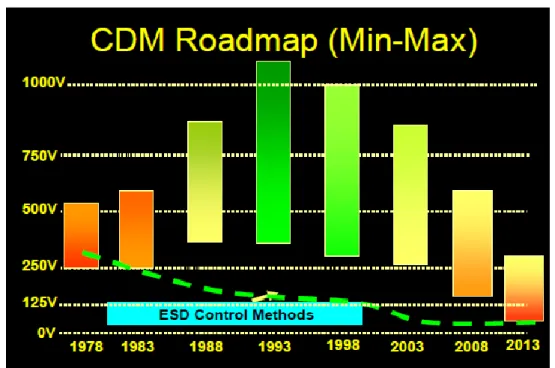
The Charged Device Model
CDM damage occurs when a charged ESD sensitive device is grounded or when a neutral device is grounded in the presence of an electrostatic field. This makes the CDM model also valid for Field-Induced Model (FIM) for both field-induced charged device (FCDM or FICDM) and field-induced charged board (FCBM or FICBM). As previously mentioned, CDM is one of the two very useful models for ESD analysis in industry. Therefore, much literature is published each year regarding ESD analysis using this model. [1], [3], [7]-[25], [30], [36], [45], [47], [49]-[51], [58]-[59], [61]-[63], [68].
In recent years, arbitrary CDM protection levels have been specified as IC qualification goals with little background information on actual/realistic CDM event levels and the protection methods available in device design for safe production of IC components. The rapid advancement of IC technology scaling, coupled with the increased demand for high speed circuit performance, are making it increasingly difficult to guarantee the commonly customer “500V” CDM specification. At the same time, the required static control methods available for production area CDM protection at each process step have not been fully outlined. Therefore, a realistic CDM specification target must be defined in terms of available and commonly practiced CDM control methods, and also must reflect current ESD design constraints. [3]
Table1 -II. Recommended CDM classification based on factory CDM control. [3]
The table above is the projection of CDM levels based on extensive manufacturing industry study. It is considered by the industry council that a safe and practical CDM passing level of 250V is realistic in the realm of increased processing speed and extended packaging size. The Council strongly recommends that products with a CDM level lower than 250V should implement additional process-specific measures for CDM control, especially during product ramp-up. [1], [3].
Again, this trend places increased responsibility in the hands of the users to both implement tighter control programs and to reduce the charging on the device/apparatus. This means that environment static charging control becomes more so important, which, again, justifies the pursuit of this work.
Figure 1.3. Charge Device Model sensitivity limit projection
In the projection of the CDM sensitivity levels (min and max) indicated in Figure 1.3, also shown is the progression of ESD control capability for CDM during the same time period. The same general arguments as given above for HBM also apply for CDM. However, the advanced designs will have a larger impact on CDM. This is because the HSS IOs (High Speed Serial Links) are generally used in high pin-count, hence larger capacitance, IC packages. This higher capacitance leads to relatively higher magnitude discharge peak current levels, and thus greater challenges in CDM protection design. A proactive implementation of advanced CDM controls would not only become necessary but would become mandatory within the next five years. [1], [3].
1.1.3 Types of damages and protection
Due to ESD pulses, usually the IC chips become damaged at the Input/Output (I/O) signal pins; the failure appears as thermal damage to the transistors. Other failures are due to:
Figure 1.4. Examples of IC ESD damages. [5]
(1) oxide breakdown of the transistor gates;
(2) system board level ESD stress, known as IEC stress,
(3) customer application stress, known as electrical overstress or EOS. [1]-[3], [5], [8]-[11], [13]-[25], [34].
These two latter threats are of particular interest for further emphasizing the importance of this work, as they can occur in the production line where high levels of charge can be present.
In advanced CMOS technologies, circuitry which connects directly to I/O pads are often most at risk of damage during a CDM ESD event [1], [3]. Therefore, from the user’s stand point, it is important to ensure charging and discharging at each manufacturing step and prevention measures should be taken to avoid the possibility of hard
Figure 1.5. Comparison of current waveforms for CDM, MM, and HBM ESD events. [3]
While component ESD stress levels are typically defined in terms of a stress voltage (2000V HBM and 500V CDM), designers consider the ESD event in terms of the resulting current waveform (Figure 1.5). Elements in ESD protection circuits and ESD conduction paths are sized based on a target peak stress current and duration. In general, if the target peak current increases, the ESD elements and conduction paths must be increased in size accordingly. [3]
In the literature [8]-[20], the aforementioned types of stress or failures have been sub-classified, as not all failures are instantaneously damaging; some are latent/functional. In the immediate failure, the effect can be readily seen by the equipment manufacturer or user. In the delayed failure, the device is damaged only up to the point where it may pass quality control tests, or it may keep functioning for, but it wears out sooner than its rated time.
It is very difficult to determine the point at which the damage due to ESD occurs, since it can take place anytime during the manufacturing process, assembly, testing, packing and shipping. ESD control program that protects the device right from the
manufacturing plant to the retailer and the user are therefore paramount. Some protective guidelines used in ESD control are established, [1]-[3], [7], [10], [12], [19]-[20], [69]-[72]:
a. Most workstations are provided with measures such as conductive table mats, wrist bands, conductive flooring, as protection of components from damage due to electrostatic charge on the body.
b. Air ionizers are operated in ESD protective areas to neutralize static charges on non-conductive materials used in the manufacturing lines.
c. All test and soldering equipment is provided with ground potential and is periodically inspected.
d. Anti-static foams are used during storage and transportation in order to protect ESD sensitive devices instead of ordinary plastic foams.
e. A number of monitoring devices, such as electrostatic alarms, electrostatic voltmeters and field meters are used to measure and control static charge on materials.
Despite high initial costs, most device and electronic apparatus companies have profited considerably by implementing ESD prevention programs. However, with the increase in device sensitivity, much of the responsibility in controlling the charging levels in the environment where the apparatus/devices are utilized is placed in the hands of the user.
1.2 Electrostatic measurements
1.2.1 ESD detection
ESD discharges induce voltages in the nearby circuits. When ESD occurs, the discharge time is usually 10 nanoseconds or less. Discharging energy in such a short interval results in the generation of broadband electromagnetic radiation, as well as in heat that damages electronic components. [3], [6]-[7], [10], [22]-[25], [29], [31], [33]-[34], [40], [47], [73]-[83]. This electromagnetic radiation—especially in the 10 MHz to 2 GHz frequency range—can affect the operation of production equipment. Much of today's complex equipment is controlled by microprocessors that operate in the same frequency range as the EMI from ESD events. ESD events cause a variety of equipment operating problems including stoppages, software errors, testing and calibration inaccuracies, and mishandling, all of which can cause physical component damage. To detect such events, EMI locators are used.
In the last years, with the advancements achieved in high frequency instrumentation, such as oscilloscopes of up to 20 GHz bandwidth, it has become easier to detect ESD events through a high frequency antenna connected at the input of a GHz bandwidth oscilloscope. A simple test at various distances from the field source could give a good indication of the ESD and EMI (Electromagnetic Interference) present in the respective environment. The schematic of the test is similar to the representation in Figure 1.5. A recorded set of waveform, obtained from three antennas, is depicted from literature. This aspect is not addressed in this work. However, since the manufacturing of filters is susceptible to ESD events, such testing can be important.
Figure 1.6. ESD and EMI; Discharge current measurement. [67]
Figure 1.7. Example of radiated EMI from a CDM ESD event detected by a set of three antennas. Source: Joe Bernier at Intersil. Cited by [78]
1.2.2 Charge measurement
The Faraday pail is a shielded cup with attached electrometer for directly measuring the charge on any object dropped into it. This device is used for the measurement of the static charge on ICs, or on any charged object, including textile materials [16], [20], [78], [84]-[88].
U q C x 0 a) AS C Izolator Izolatori EP CF -q +qx +qx b)
Figure 1.8. Faraday cup. a) principle b) measurement. [67]
The principle of the Faraday cup is illustrated in Figure 1.8. The cup CF is a metallic cylinder, insulated with respect to the ground, and EP is the protective shield. The charge to be measured, +qx, induces negative charging at the interior of the metallic wall of the cup CF. Consequently, on the exterior surface of the cup positive charges appear. These charges can be measured with an electrometer.
1.2.3 Surface potential and electric field measurements
One of the very common methods of monitoring the static charge of a dielectric film is by measuring the potential decay at its surface [84], [87], [89]-[111]. The other method is by measuring the electric field created at the surface of the charged body [84], [87], [90], [93], [107]-[114].
Regardless of the particular circuitry solution employed [22]-[23], [62], [84], [87]-[91], [115]-[118], the instruments for the measurement of the electric field are built on the same basic principle (Figure 1.9).
PM PM U Z Ex Ex +q b) a) +q -qx +qx +qx
Figure 1.9. Metal plate charged through induction. a) insulated, b) induction probe. [67]
A metal plate (PM) placed in the electric field of a positive charge, +q, charges through induction as in Figure 1.9.a, with negative charge on the side towards the source +q and positive charge on the opposed side. However, if PM is connected to the ground as in Figure 1.8.b, the positive charges flow to the ground and only the negative charges are left. Thus, in a grounded metal plate in an electric field, positive charges induce negative charging and, reversely, negative charges induce positive charging. For a plate of surface S, the induced charge by the field of intensity Ex is given by the equation:
S qx x (1.1) where x r x 0 E (1.2)
is the uniformly distributed charge density on the plate. In (1.2), r is the relative permittivity of the material between the plate and the charged object under test and 0 = 8.86 10-12 F/m is the vacuum permittivity. As E
x propagates through air, r = 1 and hence:
x
x S E
On the path through the ground, the charge qx moves through the impedance (Z). This creates a voltage drop (U) proportional to qx and hence with Ex. The recorded value for U~Ex [67], [119]-[121].
In the following examples [90] of fieldmeter and electrostatic voltmeters, the detecting element is a vibrating capacitive sensor. In this configuration, an electric current I is induced in the sinusoidally vibrating sensor. :
d d t
wt d S U t d d S dt d U dt dC U I r r sin cos ) sin( 0 1 1 0 1 0 0 (1.4)U is the difference of potentials between the tested surface and the vibrating probe, [V], d0 is a constant representing the separation between the electrode and the charged
surface under test when the electrode is not vibrating, [m],
d1 is the amplitude of vibration, [m], and ωt is the circular frequency of vibrations, [rad/s].
Figure 1.10 presents an electrostatic fieldmeter. A fraction of the detected and processed voltage Vp is inverted and fed back to a screening electrode. At this point the sensing electrode is influenced by two electric fields: one created by the tested surface and one generated by the screen. Therefore, the greater the surface voltage, the greater is the inverted voltage on the screen. Fields created by these two voltages cancel each other. Potentiometer P is used to establish a constant ratio between Vs and the measured voltage Vp. When the sum of the two fields equals zero, the stability of the signal detected by the vibrating sensor is greatly enhanced. However, the potential difference between the surface and the sensor can lead to the discharge and damage of the equipment if spacing d0 becomes too small. The value of measured Vs is also sensitive to the changes of the distance d0. [90] As mentioned before, other circuitry solutions are employed to ensure accuracy [116]-[117].
The following paragraphs are concerned with electrostatic voltmeters. Many voltage measurement applications cannot be made using conventional contacting voltmeters because they require charge transfer to the voltmeter, thus causing loading and modification of the source voltage. For example, when measuring voltage distribution on a dielectric surface, any measurement technique that requires charge transfer, no matter how small, will modify or destroy the actual data. In these types of applications a new approach to voltage measurement is needed [87], [90]
An instrument that measures voltage without charge transfer is called an electrostatic voltmeter. A primary characteristic of non-contact electrostatic voltmeters is that they accurately measure surface potential (voltage) on materials without making
contact and, therefore, no electrostatic charge transfer and loading of the voltage source can occur [89],[ 90], [91].
In practice, an electrostatic charge monitoring probe is placed close to the surface to be measured. Electrostatic voltmeters function to drive the potential of the probe body to the same potential as the measured unknown. This achieves a high accuracy measurement that is virtually insensitive to variations in probe-to-surface distances, as well as preventing arc-over between the probe and measured surface. [90], [92], [93].
An example of the electrostatic voltmeter circuit is shown in Figure 1.11. In this voltage-follower device the output of the integrator drives a high voltage amplifier circuit to replicate the voltage on the tested surface. The amplified voltage is then applied to the sensor thus nullifying the electric field between the tested surface and the sensing electrode. Potential on the electrode "follows" the potential on the surface. In this case there is no threat of the eventual discharge between the probe and the surface under test, even at close spacing. This ability of following the voltage makes the electrostatic voltmeter measurement independent of the distance d0 at least within a
certain range of d0. If the span between the surface and sensor is too big, the probe becomes influenced by other electric fields present in the vicinity [84], [87], [90].
Figure 1.11. Electrostatic voltmeter (voltage follower). [90]
Figure 1.12. AC-feedback electrostatic voltmeter. [90]
The AC-feedback in voltmeter Figure 1.12 uses a different technique to achieve spacing independent surface voltage-charge measurements. Rather than cancelling the Kelvin current I by use of a feedback DC voltage which follows the surface test voltage to produce zero electric field, the AC feedback method utilizes a nullifying current I' to zero the Kelvin current I. The current I' is produced by external generator circuit tuned to the frequency of the Kelvin sensor oscillations:
dt dV C
I' t (1.5)
Therefore, when currents I and I' cancel each other, I = I’,
dt dV C dt dC U t (1.6)
As both I and I' currents are inversely proportional to spacing d0, the ratio of the amplitude of Vt to U (the DC test surface voltage) remains constant over the large range of d0. As shown in Figure 1.11, the Vt signal is obtained by amplification of the current I converted to a voltage at the preamplifier. At high gain, the current I is being cancelled to a very small value.
Figure 1.13. d0 effect on fieldmeter and electrostatic voltmeter measurements. [90]
The graph in Figure 1.13 presents a comparison of measurement errors for a standard fieldmeter and the Trek model 520 electrostatic voltmeter. The experimental data was acquired from the factory-calibrated fieldmeter at one inch distance from the
object that is being measured. The reason for the fieldmeter error is that the probe, a copper disk of 9.9 cm diameter (310 square cm surface area), connected to 1 kV DC source, was placed at distance different from the factory specifications. As you get closer to the surface, the field increases, with the surface potential being constant. The only way to make correct measurement with the fieldmeter is to re-calibrate it every time the distance of the fieldmeter vs. the surface is changed. The experiment indicates that it is important to keep the appropriate spacing between the fieldmeter sensor and the tested surface in order to consider the measurement reliable.
Table 1-III shows a brief comparison between fieldmeter, electrostatic voltmeter and AC feedback electrostatic voltmeter. Because of their principle of operation, the electrostatic fieldmeters are suitable for measurements conducted on relatively large areas. They are also not as accurate as electrostatic voltmeters. Since the results provided by the fieldmeters depend strongly on the probe-to-surface distance d0, it is more convenient to read them as the electric field intensity values (thus the name, fieldmeter). Magnitude of fields measured this way is usually high.
Electrostatic voltmeters, particularly the voltage followers, can be employed for tests of relatively small charged areas - they have much better resolution than fieldmeters. Voltmeters are also very accurate over a certain range of distances d0. Since the potential on the sensor during the measurement is theoretically equal to the potential of the tested surface, there is no hazard of discharge.
Table 1-III. Fieldmeter and electrostatic voltmeter comparison [90]
The above suggests the person conducting measurement has to be aware of the high voltage present on the probe and proceed with caution. AC-feedback voltmeter is a low-cost alternative for the voltage follower type voltmeter. It does not have high voltage circuitry and is accurate within a certain specified range of distances d0. For example Trek's model 520 holds the 5% accuracy over the distance between 3 and 30 mm [90], [91].
1.3 Conclusions
With the physical limitations attained in the very last years in processing speed, and the industry’s stumble to find novel design solutions both at the circuit level and in circuit cooling, ESD susceptibility of electronic devices has increased significantly. As the industry council has recently proposed that the safe ESD voltage levels be lowered [1],
new solutions should be found to ensure the equipment functionality, and personnel safety, justifying the importance of the present work.
The evaluation of ESD risks requires accurate measurement of the charge carried by the human operator or by the various objects on the manufacturing line. The fieldmeters and the electrostatic voltmeters enable the non-contact measurements required by ESD risk monitoring in an industrial environment. The literature-based comparison between these two classes of instruments indicates that they meet the methodological requirements of the present study.
2 INSTRUMENTS AND METHODS
I have no satisfaction in formulas unless I feel their arithmetical magnitude. Baron William Thomson Kelvin
his chapter presents five proposed methods for the measurement of electrostatic charging on textile materials. The first method is linked to the HBM model discussed in chapter one, while the second involves a novel instrument for indirect measurement of the charge on the personnel. The last three measurement methods presented in this chapter are used for evaluating the charging state of non-woven textile materials that can attain hazardous levels of static charge during the manufacturing process.
2.1 Measurement method for static charge generated at walking on an insulating carpet
In the background chapter, the HBM was referred to as one of the two most important models for assessing the potential hazards to devices and electronic equipment. In fact, up to the point of the skyrocketing of high-speed circuit demand on device operation, the HBM model preceded the CDM model in hazard significance. The recent technology roadmap [1] does emphasize the continuing significance of assessing the personnel charging and exemplifies the signal monitored during walking. The roadmap, the extended previous industry council report on HBM [2], as well as publications [19], [55]-[56] and standards [70], [122]-[124] recognize that such monitoring continues to not only be important but also challenging to implement and control.
2.1.1 Mechanisms, phenomena and HBM
When two insulating materials A and B (eg. an operator’s shoe sole and a textile or PVC floor covering) come in contact or rub against each other (Figure 2.1.a), charge transfer occurs between the two materials until the electrical balance at the contact surface is attained. If A loses electrons, it becomes positively charged while B, which receives these electrons, becomes negatively charged. If A is quickly separated from B, A remains positively charged and B keeps its negative charge (Figure 2.1.b).
Finally, if A keeps a contact point (or touches again) with B (Figure 2.1.c), the charge remains the same. Figure 2.1 shows the step-by step mechanism of personnel charging while walking on an insulating floor. In such process, the contact charging phenomenon is shown to always be accompanied by rubbing between the two contact surfaces, which causes tribocharging (Figure 2.1.c ).
Personnel tribocharging may occur while: (1) Walking on insulating floor carpets (2)
Changing synthetic fiber garments (3) Sitting on a chair (4) Dusting desk or apparatus
The concern with discharges produced by charged personnel when touching a device terminal or apparatus is that circuit damage can occur. The zapping effect is also unpleasant for the operator. Therefore, it is important to analyze the most frequent situations in which the charging of personnel (P) can occur. Figure 2.2 presents the personnel’s typical charging at walking on an insulator floor-covering. Both positive and negative charges may appear on his clothes, depending on the fabric parts that came in touch (clothes, shoes, floor. etc). It is important to keep in mind that the charges are accumulated only on shoes and clothes, while the body, rather conductive, serves only for the charge transmission process (eg. through the fingers, as in Figure 2.2.b).
In 2.2.b, the typical tribocharging of the personnel at the workbench is shown. Here, the charging occurs at rubbing with the chair, as well as between the shoes-soles and the insulator floor-covering (CP). This charge is added to the charge accumulated while walking to the working area shown in Figure 2.2.a. Hence, due to the multiple sources of static charging that the personnel is exposed to, the charge accumulates on the body system and electrostatic discharge (ESD) may occur between the person’s finger and an apparatus (Figure 2.2) or device (Figure 2.3).
Figure 2.3. Induction charging a) phenomenon b) and c) practical examples
Besides the contact charging and tribocharging, charging through induction can occur in electronic industry and manufacturing lines, as stated in chapter 1. When a charged body, A, comes near a metallic non-grounded body (B) (Figure 2.3), the B1side
positioned near to A charges with opposite charges. Only if A is moves far enough from B, the induced charge on B can decreases to zero. When the electric field intensity (between A and B)
(2.1)
is high (500–1000 kV/m) and the IC has a grounded pin (Figure 2..c), then an ESD can occur between A and B , which can cause destructive, latent or functional IC damage due to the induced voltage on the pin and the discharge current created on the path to the ground.
Finally, an operator’s high tribocharging, to levels of over 5-15 kV, can also occur at changing a garment or piece of clothing. The tribocharging level depends on the speed of movement, as well as of the materials’ positions in the triboelectric series.
As mentioned in the background chapter, throughout this work the simple HBM model, illustrated in Figure 2.c, is used. In this diagram, RP represents the equivalent resistance of the body, and CP the equivalent capacitance. CP includes the capacitance
between shoes and ground (CTG), as well as the body capacitance with respect to the ground. In this simplified model, the assumption is that CP is the capacitance of a sphere of surface equal to the body surface.
CP varies in large limits (100-250 pF) depending on soles material (T) and floor-covering type (CP), as well as the body weight. [19], [56]. In the theoretical calculations, the standard values CP = 200 pF and RP = 1.5 KΩ are first assumed, and then CP is determined experimentally. Theoretically, knowing CP and the accumulated charge in CP, q, the voltage on the body and the charging energy accumulated on CP can be derived using the formulae:
(2.2)
(2.3)
The scenario of personnel (P) charging at walking on an insulating floor-covering is further theoretically analyzed [14], [16], [30], in the methods paragraph and the results presented in Chapter 3. However, the involved mathematics is complex and, due the simplifying assumptions and constraints, as well as the uncontrollable parameters, such Cp, the results are not convincing enough. The simplest and most effective method to analyze this problem [16]-[17], [19], [64], [85], [125] is through experimental approach. In practice, UP and CP are first measured then q is computed. In the next paragraphs, the experimental setup for these measurements is presented, followed by the proposed measurement method [126].
2.1.2 Experimental setup and instrumentation
The experimental setup is presented in Figure 2.4.
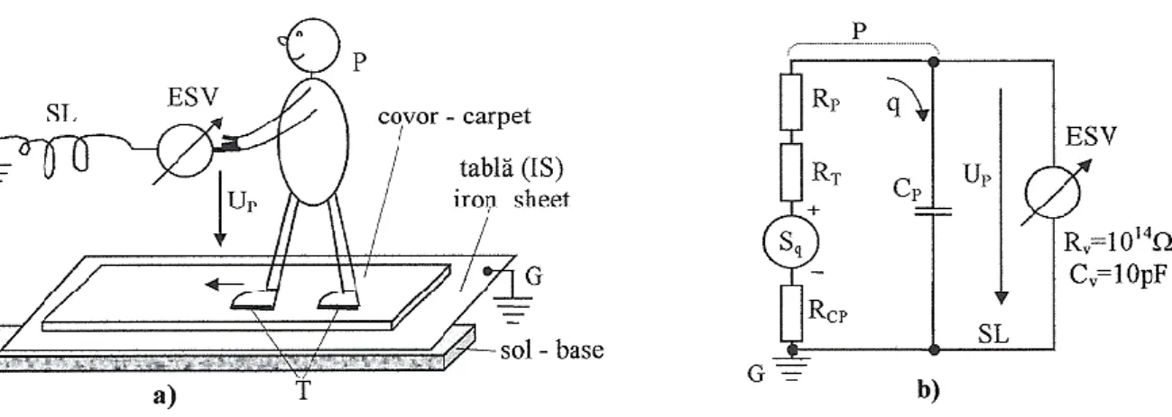
Figure 2.4. Proposed method for Up voltage measurements: a) physical setup b) equivalent diagram
The Electrostatic voltmeter (ESV) is a Field Mill type voltmeter [22]-[23], [125] with the following characteristics: nominal voltage 0.2 kV, 2 kV and 20 kV, input resistance RV >1014 Ω and input capacitance CV>>10 pF, accuracy 3 % end of scale. Starting from here
on, RV > RCP + RT and CV << CP, which means that the voltage UP indicated by ESV is accurate. The meter is equipped with the hygrometer function. Thus, the air humidity in the working area is constantly monitored. The physical setup in Figure 2.4.a was placed at constant temperature and humidity: 22°C and RH = 50% in an atmosphere with no air flow.
Two types of insulating floor coverings (CP) are used and tested:
• PCV, a typical material used in electronic areas and some assembly lines;
• Polypropylene carpet, a typical material used in many rooms in office and
industrial setting.
Two shoe soles were tested:
• classic shoe type, with sole of man-made (synthetic) material(T1); • sport shoe type, with neoprene rubber sole (T2).
Figure 2.5. Diagram for carpet resistance measurement.
Figure 2.6. Measurement of capacitance CP
Men of comparable bodyweight were chosen for the test, typically 75 kg, knowing that CP increases with bodyweight [64]. Otherwise, this election was made based upon the most disadvantageous combination of conditions from amongst those shown above.
For both CP types, the insulating resistance RCP is measured using the capacitor method [67]. The diagram for the carpet resistance and the body capacitance measurement is shown in Figure 2.5 and Figure 2.6, where 1, 2 are circular electrodes, C is a capacitor of known value and U0 = 1 kV is the test voltage.
The personnel’s (P) capacitance, Cp, was measured with both shoe types (T1 and
T2). As support for the P's path, a PVC carpet (CP1) and a polypropylene carpet (CP2)
were used. The results for the RP and CP measurements, derivation of the charge accumulated during walking at different combinations of materials, are presented in subchapter 3.1.
2.1.3 Proposed measurement method
The measurement methods for the personnel tribocharging during the first three activities mentioned in the previous paragraph are investigated here. The level of charging is expected to depend on the distance of the materials in the triboelectric series shown in chapter1. The experimental setup proposed for testing the method is shown in Figure 2.4, and is a modified and improved version of the classical method.
In order to explain the proposed method, first it is necessary to briefly overview the classical method, which we modified. In the classical measurement method [64], the test person walks on an insulating floor positioned onto a grounded conductive surface. During the measurement, the tested person is connected to an electrostatic voltmeter through a 5 m coaxial cable and a hand-held metal electrode. The test procedure is as follows. The test person walks on the floor at 2 steps/sec and the electrostatic voltmeter to which is connected measures the voltage on the equivalent capacitance of the parallel structure CP, CCX (coaxial cable capacitance), and CV (input capacitance of the voltmeter). The main drawbacks of this classical method are introduced by the coaxial cable between the tested personnel and the voltmeter:
- The capacitance Ccx (500-600 pF) can be greater than CP (≈ 200 pF), hence the voltage U indicated by the ESV can be smaller than the real parameter UP. Obviously, using (2.1) and (2.3) we can still derive UP:
(2.4) However, the measurement method may be inconvenient, as all the theoretical verification is not the user preferred method and can be inefficient.
- The capacitance Ccx, (more than 5 m in length), may become a parasitic source due to the cable bending and torsion operations during the test.
The proposed method is an improvement of the above classical method. The experimental setup remains the same as in the classical solution, which means that the test person (P) walks on an insulator carpet (CP) positioned on a grounded conductive surface (IS).
The difference resides in eliminating the parasitic capacitance introduced by the coaxial cable. In the adopted solution shown in Figure 2.4.a, the ESV is grounded through a supple connection, a wire (SL), connected to the ESV ground terminal. This way, CCX from the classical method is eliminated, and so is a big source of measurement error or uncertainty for the user. By comparison, the grounding wire, SL, in the proposed solution does not affect the UP equation. Moreover, the voltage UP at the body-system terminals is measured directly at the ESV input, which is another important advantage of the proposed method.
Figure 2.4.b shows the equivalent diagram of the experimental setup illustrated in Figure 2.4.a. In the equivalent diagram, Sq represents the electric charge source (q), that
occurs at the friction between the shoe-sole (T) and the insulating carpet during walking. CP, the P's capacitance, charges from Sq via the shoe sole resistance (RT) and the body resistance (RP =1.5 k ohms) which is negligible compared to RT (109-1012ohms). Sq
is connected to the ground via the floor-covering resistance (RCP), which is within the same range as RT (or higher).
In an earlier paragraph, it was specified that body-system calculations for the resistance and capacitance can be performed if the voltage at the body-system terminal is known. The basic equations for these calculations are presented next.
At each step when the sole is lifted from the floor-covering, CPis charging via the sole resistance RT:
(2.5) where
(2.6) represents the time constant and UPm-the maximmum value of UP (Figure 3.1). Between two steps, CP is discharged via carpet resistance RCP:
(2.7)
where:
(2.8) represents the charge decay time constant. From (2.4) and (2.5), if
(2.9) the human operator cannot charge (or charging is lower than for RT< RCP). This is because the Cpdischarging speed is greater than its charging speed.
2.2 Faraday pail-based instrument for measurement of the electric charge of textile materials
This subchapter describes a Faraday cup based instrument designed to measure the electrostatic charge on textile materials, as well as protective clothing used in the electronics industry. The proposed Faraday instrument is different from the classically used type [126], as there is no direct electrical contact involved with the sensor electrode. This eliminates the cable between the electrode and the measuring instrument that is a main source of noise. The measurement method is explained (§ 2.2.1), its mathematical equation derived (§ 2.2.2) and the technical characteristics of the instrument detailed (§ 2.2.3). The characteristics of the built instrument are presented in § 3.1.2.
As mentioned in the previous subsection, the measurement of the accumulated charge (q) on a body system is typically performed through a “walking” circuit that includes the RC impedance of the HBM, as in Figure 2.2.c. The impedance of this RC model has considerable variations and instabilities, which contribute to errors in the measurement result. To avoid this limitation, a different method of measurement of the electrostatic charge is proposed. This proposed method not only can be used to measure the charge on the personnel, but also to measure the charge on either woven or non-woven textile materials of bigger size.
The method for the operator charge measurement consists of measuring the triboelectric charge accumulated on the piece of clothing (vest, pullover, etc.) that the person takes off in preparation to working at the workbench (and handling sensitive
electronic components). To measure the value of the charge (qx) the authors built a Coulombmeter-type Faraday Cup. The method is described in detail the next section.
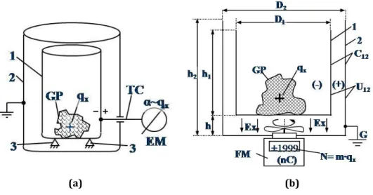
2.2.1 Proposed method and diagram
As previously mentioned, when rubbing two objects (A and B, Figure 2.1.a) they charge with opposite sign charges of the same value (+qA=-qB). Figure 2.7 above suggests that after the object separation (Figure 2.7.b), the qx measurement is possible by measuring the charge on either object A or B. Based on this observation, the charge accumulated on the personnel during the work preparation can be the same as the charge accumulated on the piece of removed clothing (qGP, Figure 2.8). This charge will be designated as qx.
A classic [22] Faraday Cup Instrument (Figure 2.8.a) can be used to measure the accumulated charge qx. The active electrode (1) picks up the static charge (+qx) accumulated on GP and transfers it to the electrometer (EM), which displays a value proportional to qx.
(a) (b)
Figure 2.8 Faraday Cup Instrument. (a) Classic instrument. (b) Functional diagram of the proposed instrument
However, the main limitation of this classical method is that the triaxial cable (TC) between the electrode and the electrometer can often cause important measurement errors during instrument handling [128].
The diagram of the proposed instrument is shown in Figure 2.8.b and the labeling previously assigned to the elements in Figure 2.8.a is preserved. For the sake of simplicity, the insulators 3 have been omitted from Figure 2.8.b. FM is a Field Mill type instrument [67], of the same characteristics as previously presented in subchapter 2.1, that measures the electric field Ex produced by the charge to be measured, qx. The displayed number N is directly proportional to the charge qx and, as shown, the measurement is made without direct contact with the electrode 1. Through this method, the triaxial cable (TC in Figure 2.8.a) is eliminated from the measurement circuit and, consequently, so is the main limitation associated with it [129].
2.2.2 Measurement equation
The measurement equation of the proposed instrument can be determined from the observation that when electrostatic charge (qx) is present on the object GP, the potential between the two armatures 1 and 2 of the capacitor C12 is mathematically expressed by the formula:
(2.10) Consequently, between the two bases of the cylinders 1 and 2, an electric field will occur: h U Ex 12 (2.11)
where h is the distance between the two cylinder bases. The field intensity Ex is numerically displayed on the Field Meter FM:
(2.12) The letter a in Equation (2.12) symbolizes the fieldmeter sensitivity. The mathematical equation for the instrument is derived by substitution of (2.10) and (2.11) in (2.12):
(2.13) where the constant m is the instrument sensitivity:
2.2.3 Instrument Calibration and Error Calculation
The instrument was designed as a two-range measurement system: 200 nC and 2000 nC. Since the charge qx cannot be measured directly (unlike a voltage or a current for example), qx was calculated using the mathematical expression (2.9). For a capacitance C12 of 140 pF, the two full ranges labeled “max” for future references correspond to the voltages U12 of 1.43 kV and 14.3 kV respectively.
The calibration diagram is shown in Figure 2.9, where VS is an adjustable voltage source and DV is a digital voltmeter of high precision (±0.02%). All the other notations from Figure 2.8 are kept. From the mathematical expression (2.13), it results that m can easiest be adjusted by modifying the fieldmeter sensitivity, a. The double range calibration was possible by adjusting the gain of the fieldmeter.
Figure 2.9 Instrument Calibration
From the elements in equation (2.14), the total error of the instrument in Figure 2.8.b is calculated through the method described in [67], vol. 1, pp. 33-239:
h h C C a a m m 12 12 (2.15) where, Δa/a is the fieldmeter error (Δa/a1.5%·max), ΔC12/C12 the determined capacitor error (ΔC12/C12 ≤ 0.5 %) and Δh/h represents the relative error introduced by the
equation (2.13), taking into account the simulation error Δqx/qx ≤ 0.5 %), the calculated maximum error introduced by the instrument is 2.7%. This establishes the basic methodological index for the practical applications of this measuring instrument: the precision class 3. The physical and performance characteristics of this instrument are detailed in subchapter 3.2.
2.3 Measurement method for the personnel charge on the assembly line
The present subchapter describes a measurement method of the electrostatic charge on textile materials and personnel clothing. As described in subchapter 2.2, static charge can also be created on a garment as a result of removing it from a human body, usually before sitting at a workbench and handling PCBs, ICs, etc. The method is based on charging a capacitor of known value with the triboelectric charge accumulated on the garment placed in a Faraday cup (FC) right after being removed off of the body system.
The capacitor, charged with the charge to be measured, is part of the feedback loop of a circuit with operational amplifier with an Electrostatic Voltmeter as load. The charge is calculated as a function of the capacitor value and the voltage indicated by the output electrostatic voltmeter.
2.3.1 HBM testing method
As earlier stated, the measurement concerns the triboelectric charge (q) accumulated on the human operator (P, Figure 2.10.a) while removing a garment (GP: coat, jacket, sweater, etc.) as in Figure 2.10.b, before sitting and starting working at the workbench or worktable.
(a) (b) (c)
Figure 2.10. The Human Operator (P). a) Wearing a sweater (GP). b) Electrostatically charged from removing the sweater c) The model for the Human Body. [128]
Figure 2.10.c reiterates the HBM model for the purpose of present work. Here, CP is the equivalent capacitance of the person with respect to the ground (G) before removing the piece of clothing. CP is the sum between the capacitance of a sphere of surface equal to the surface of the operator body with respect to the ground, CS, and additional parallel capacitors, CΠ [128]. Mathematically, that is:
C C
CP S (2.16)
In practice, CP varies within a wide range, as CS depends on the size of the person P and the type of clothing worn. Moreover, CΠ is a function of the surrounding conductivities, thus calculating the two terms of CP is a rather laborious task and the result insufficiently accurate. All these considered CP is initially adopted as equal to 200 pF and then experimentally measured using the diagram shown in Figure 2.11. This setup is similar to that used in the already presented case of walking on a carpet.
Figure 2.11. Diagram for the Human Body capacitance, CP, measurement.
The capacitor C of known value is first charged to the voltage U0, then is connected in parallel to the human body capacitance CP. The voltage U indicated by the Electrostatic Voltmeter (ESV) is then used in the calculation of the person’s capacitance,
CP:
0
1 U U C CP (2.17)This measured value is the value of the voltage that needs to be taken into account when evaluating the possibility of the ESD occurrence between the human operator P and an electronic board, integrated circuit or system, as previously stated
2.3.2 Direct method for human body charge measurement
The proposed method for the measurement of the triboelectric charge accumulated on the Human Body at the removal of a piece of clothing is based on the principle of charging a capacitor of known value (C) with the electrostatic charge to be measured (qx). The method was experimented both by using direct and indirect measurements, cases in which the charge to be measured was named q1 and q2 respectively. Both methods, as well as the reason for finally choosing the indirect measurement method, are presented in the next paragraphs. The diagram for the direct measurement of the triboelectric charge (q1) is shown in Figure 2.12.
Figure 2.12. The direct method of measuring the static charge after garment removal.
The experimental setting showed in Figure 2.12 was placed in an environment of constant temperature and relative humidity, 22˚C and 50% (RH) respectively. The environment was specific to the computer and electronics laboratories.
The same Electrostatic Voltmeter, of fieldmill type and digital display, with the following characteristics: 0.2 kV, 2 kV and 20 kV scale, 2 % accuracy, 106 Ω input
resistance and 100 pF input capacitance is used, as previous. The capacitor C is of high precision, specific for instrumentation, and adjustable within the range of 30 pF-500 pF.
The procedure for the direct measurement is performed as follows: the human subject (P), removes an outdoor piece of clothing (wool jacket, for example) as in Figures 2.10.a and 2.10.b, and then rapidly places it into a metallic container (Figure Figure 2.8 and Figure 2.13.b). With his index finger (F), the subject touches the free terminal (B) of the capacitor C (Figure 2.12).
As a result, the charge q1 created on P at the removal of the piece of clothing, GP, is transferred to the capacitor C which, charges at its terminals with the voltage U1. The
Electrostatic Voltmeter, ESV, of capacitance CV<<C, CP, indicates this voltage U1. Since all three capacitors are in parallel, the measurement equation is of the form:
11 C C U
q P (2.18)
Five students (A, B, C, D, E) were used as test subjects, all equipped with the same type of clothing: synthetic sweater (wool type) over synthetic fiber, cotton-type shirt. The synthetic materials of the two pieces of clothing were chosen such that they would be as far as possible on the triboelectric series, in order to obtain maximum triboelectric effect. Each subject was initially discharged by touching, with both hands, a metallic piece connected to ground.
2.3.3 Indirect method for human body charge measurement
According to the triboelectric charge conservation principle, and as suggested in § 2.2.1, the charge q2 that accumulates on the personnel garment or piece of clothing at fast removal is equal and of opposite sign to the charge q1 left on the operator body P. Consequently, the result of measuring the charge (-q2) accumulated on the piece of clothing indirectly indicates the absolute value of the potentially damaging human body charge of interest, q1.
The general diagram for the indirect measurement of the triboelectric charge (q2) is shown in Figure 2.1.3 below. The Faraday Cup (FC) device is comprised of two cylinders, one for measurement 1 and the other one for shielding 2, insulated with respect to each other through the insulator 3. The switch K serves to discharge of the capacitor C before starting the experiment.
Figure 2.13. The indirect method of measuring the static charge after garment removal
In the indirect method, the subject/the operator, removes the piece of clothing (GP) and rapidly throws in cup 1. The triboelectric charge q2 accumulated on GP is transferred to cup 1 and the voltage U2 is measured..
The measurement equation is of the form:
2
2 CU
q (2.19)
2.4 Surface potential versus electric field measurements for charging state characterization of non-woven fabrics
Surface potential and electric field measurement techniques are widely used for the investigation of the corona charging [107], [130]-[137] of dielectric surfaces in a wide range of industry applications [138]-[140]. The aim of the present work [141] is to estimate which of these techniques are the most appropriate for characterizing the charging state of non-woven fibrous dielectrics, and point out the “noise factors” that might distort the results of the measurements.
The experiments were performed on samples of non-woven polypropylene (PP) sheets, in contact with or at a well-defined distance from a grounded plane. The effect of the variability of the position of the probes with respect to the samples was also investigated. Several recommendations have been formulated regarding the use of these techniques for monitoring the charging state of non-woven fabrics in industry applications.
2.4.1 Materials and method
“Standard” square samples (100 mm x 100 mm) were cut from non-woven sheets of PP (sheet thickness: 400 m, average fiber diameter: 20 m, as a detail shows in Figure 2.14).
Figure.2.14 Photograph of the non-woven polypropylene media.
The samples shown in the previous figure were placed on an aluminum plate connected to the ground as shown in Figure 2.15.a and Figure 2.16. The sample carrier consisted of a PVC plate, to which the assembly plate electrode + non-woven fabric was firmly attached. A conveyor belt supported the sample carrier and transferred it from
20µm
the charging position to the surface potential measurement and to the electric field measurement positions. The accuracy of horizontal positioning of the conveyor belt is 0.2 mm, and the positioning accuracy of the probes is 0.1 mm. The total geometrical error of the setup is less than 5%.
The samples were charged using the negative corona discharge generated by a high-voltage wire-type dual electrode as in [130], facing a metallic grid (Figure 2.15.b) distanced at 15 mm from it and located at a fixed distance (30 mm) above a grounded plate electrode (aluminum; 165 mm x 115 mm), as shown in Figure 2.15.
(a) (b)
Figure 2 Electrode systems employed for the corona-charging of non-woven media (all dimensions are in millimeters); (a) triode-type arrangement; (b) aspect of the grid electrode (grid wire diameter: 1.18 mm).
The high-voltage electrode consisted of a tungsten wire (diameter 0.2 mm) supported by a metallic rod (diameter 26 mm) and distanced at 34 mm from its axis. The wire and the cylinder were energized for 10 s from an adjustable high-voltage supply
4 mm mmm m
![Figure 1.4. Examples of IC ESD damages. [5]](https://thumb-eu.123doks.com/thumbv2/123doknet/7955917.266535/20.892.159.732.147.456/figure-examples-ic-esd-damages.webp)
![Figure 1.5. Comparison of current waveforms for CDM, MM, and HBM ESD events. [3]](https://thumb-eu.123doks.com/thumbv2/123doknet/7955917.266535/21.892.147.747.137.421/figure-comparison-current-waveforms-cdm-hbm-esd-events.webp)
![Figure 1.8. Faraday cup. a) principle b) measurement. [67]](https://thumb-eu.123doks.com/thumbv2/123doknet/7955917.266535/25.892.187.713.134.376/figure-faraday-cup-principle-b-measurement.webp)