POLYTECHNIQUE MONTRÉAL
affiliée à l’Université de MontréalGrowth control and study of ultrathin silver films for energy-saving coatings
SOROUSH HAFEZIAN Département de Génie physique
Thèse présentée en vue de l’obtention du diplôme de Philosophiae Doctor Génie physique
Mai 2019
POLYTECHNIQUE MONTRÉAL
affiliée à l’Université de MontréalCette thèse intitulée :
Growth control and study of ultrathin silver films for energy-saving coatings
présentée par Soroush HAFEZIAN
en vue de l’obtention du diplôme de Philosophiae Doctor a été dûment acceptée par le jury d’examen constitué de :
Michael WERTHEIMER, président
Ludvik MARTINU, membre et directeur de recherche
Stéphane KÉNA-COHEN, membre et codirecteur de recherche Sjoerd ROORDA, membre
DEDICATION
ACKNOWLEDGEMENTS
First and foremost, I would like to express my gratitude to Professor Ludvik Martinu and Professor Stéphane Kéna-Cohen, for accepting me as their student and for their guidance throughout this doctoral program. Their continuous support gave me the liberty to conduct my research in a way that has shaped my scientific abilities.
I would like to thank Professor Jolanta-Eva Klemberg Sapieha and Professor Remo A. Masut for their advice and encouragements.
I have had the privilege to work and exchange with many outstanding people that I am lucky to call friends. Many thanks to Amaury Kilicaslan, Thomas Poirié, Michael Laberge and Erwens Broustet for sharing the office and the laughs during all those years. Thanks also to Francis Blanchard, Simon Loquai, Fabrice Pougoum, Julien Gagnon, Hubert Camirand, Jincheng Qian, William Trottier and Thomas Schmitt. Many thanks to my colleagues from the LNMP laboratory, Arvi Sridharan, Fabio Barachati, Julien Brodeur, Elad Eizner, Zia Ullah Khan, our weekly Indian traditions and the week-end in Boston will never be forgotten.
I would like to thank Francis Turcot, and Sébastien Chénard for supervising all the laboratory work and system maintenance, making sure my experiments were always running.
I would like to express my gratitude to Dr. Richard Vernhes, Oleg Zabeida, Bill Baloukas and Josianne Lefebvre for guiding me through my scientific works, their teachings and various exchanges.
I would like to thank two very close friends, Bigdan Lulei Cirap and Odysseys Tousanov for their moral support throughout this journey.
Last but certainly not least, I would like to thank my parents for believing in me and letting me do what I love.
RÉSUMÉ
Les couches minces fonctionnelles jouent un rôle prépondérant dans la plupart des secteurs industriels actuels. Ils peuvent aussi bien être une partie intégrante d’un dispositif (cellule solaire, diode électroluminescente, photodétecteur, Laser, capteur thermosolaire, cellule thermoélectrique et bien d’autres), ou bien y amener de nouvelles fonctionnalités (revêtements résistants à la corrosion, l’usure et l’érosion, revêtement antireflet). La montée rapide de cette science est à l’origine d’un développement tout aussi rapide des techniques de dépôt et de synthèse de couches minces. Aujourd’hui, la croissance d’une couche mince avec une précision au nanomètre peut être effectuée par un simple couchage à lame au sein d’un laboratoire de recherche aussi bien que par des techniques d’évaporation dans des chambres à vide industrielles à grande échelle.
La facilité d’accès aux techniques de dépôt ainsi que l’envergure des applications scientifiques et technologiques font des couches minces une solution potentielle pour beaucoup d’enjeux technologiques et de sociétés. Certainement, un des plus grands enjeux actuels est le problème de la consommation énergétique à travers le monde et qui peut seulement qu’empirer si aucune solution convenable n’est adoptée. Une approche afin de contrer cette consommation énergétique est de modifier les vitrages architecturaux dans les bâtiments commerciaux et résidentiels en revêtant une fenêtre avec une couche réfléchissante la chaleur afin de réduire de façon drastique les charges de chauffages et de refroidissement. Le recouvrement des fenêtres par de fines couches optiques se fait par des chambres de dépôts montées en ligne, souvent jumelées avec la production du verre flotté. Bien que le maintien et l’installation de ces systèmes de dépôt est d’un grand intérêt et pose de nombreux défis, le travail de recherche présenté dans cette thèse se penche sur le mécanisme de croissance des couches minces d’argent déposé en phase vapeur par assistance plasma pour les filtres à basse émissivité. Le projet est mené en collaboration avec Guardian
Industries dans le cadre des vitrages à économies d’énergie.
Les couches minces d’argent possèdent des propriétés physiques changeantes dépendamment de leur mécanisme de croissance ainsi que de leur épaisseur. Elles ont tendance à croître en îlots en dessous d’une épaisseur critique et convergent vers une couche réfléchissante la radiation infrarouges. Cette épaisseur critique se nomme le seuil de percolation et dépend fortement de la couche sous-jacente. De plus, le caractère catalytique de l’argent fait en sorte qu’il est hautement
susceptible aux espèces réactives présentes dans le plasma ainsi que les groupes carboxylés présents dans l’atmosphère. De ce fait, une couche protectrice doit être employée afin de protéger les propriétés optiques et électriques de ces couches d’argent. Afin de mieux comprendre le processus de croissance de ces couches minces, nous avons développé une méthode optique non invasive afin de déterminer le moment précis de la transition des nanoparticules d’argent en couche continue. Cette étape est mieux connue sous le nom de seuil de percolation et est caractérisée par un changement drastique des propriétés optiques et électriques. On démontre que les surfaces ayant une énergie plus élevée (ou un caractère plus métallique) promeuvent une croissance par couche tandis que les surfaces possédant une énergie moins élevée (un caractère diélectrique) facilitent la croissance de l’argent par îlot. À titre d’exemple, en utilisant une couche de stannate de zinc on peut réduire le seuil de percolation par 18% comparativement à l’oxyde de zinc et de 80% comparativement au dioxyde de silicium.
Les atomes d’argent réagissent aisément par échange d’électrons afin de former des composés moléculaires. Le sulfure d’argent est un exemple de composé qui se forme lorsqu’un atome de soufre et d’argent forment un lien covalent. On démontre la formation d’une couche mince d’argent sur une monocouche à base de thiol, le 3-mercaptopropyl)trimethoxylosilane (MPTMS). La formation de lien chimique sur la surface inhibe la formation d’îlots et permet la formation de couches ultraminces d’argent. À partir de ce traitement, il est possible d’obtenir des couches minces possédant des propriétés d’argent massif pour des épaisseurs de seulement 7 nm, beaucoup moins que ce qu’on aurait pu obtenir en utilisant des couches de croissance possédant une haute énergie de surface. De plus, on a démontré la formation de la monocouche de liens thiol sur une couche de nitrure de silicium afin de créer un empilement à trois couches à basse émissivité avec d’excellentes propriétés de réflexions de radiation infrarouge. L’environnement plasma utilisé pour déposer les couches minces peut être riche en espèces réactives et autres contaminants. Suite au dépôt de la couche d’argent, une couche protectrice est nécessaire avant de déposer des couches d’oxydes. Si les espèces réactives telles que l’oxygène dissocié à l’intérieur du plasma parviennent à la couche d’argent à travers la couche protectrice, des dommages irréversibles peuvent être amenés à la couche d’argent. En utilisant des techniques de caractérisation de surface précises, on démontre que ce processus de dégradation est initié par la migration des atomes d’argent à travers la couche protectrice, un processus très similaire à l’effet Kirkendall. De plus, on démontre qu’en utilisant
un traitement de surface de MPTMS afin de créer les liens soufre-argent, la migration des atomes d’argent est hautement réduite (jusqu’à 20x) comparée à une surface non traitée.
Finalement, nous développons une méthode de suivi optique afin de contrôler les propriétés optiques de nanoparticules d’argent en changeant de façon précise leur environnement diélectrique ainsi que leur distribution de tailles. On démontre ainsi une façon simple de synthétiser des nanoparticules à enveloppe en plaçant des nanoparticules d’argent incorporées dans une couche protectrice dans un plasma réactif. En contrôlant de façon précise la passivation de la couche externe, on démontre qu’il est possible d’obtenir des nanostructures de type noyau-enveloppe. De plus, nous démontrons l’effet de la température du substrat sur croissance et diffusion des nanoparticules. En dessous d’une certaine température, les atomes d’argents peuvent se détacher des agglomérats pour continuer de diffuser sur la surface jusqu’à atteindre un site de nucléation stable. Au-dessus de cette température, les atomes d’argent atteignent un équilibre et la diffusion en surface est inhibée.
ABSTRACT
Functional thin films play a key role in almost all industries today. They can either form an integral part of a device (as heat-reflectors, solar cells, light-emitting diodes, photodetectors, lasers, thermal collectors, thermoelectric cells and many more) or bring additional coating functionalities (such as corrosion, wear and erosion resistance and antireflective coating). The rapid development of thin film science has led to the equally fast growth of thin film deposition techniques. The coating of a surface with precisions in the nanometers can be conducted by simple blade coating in a laboratory setting or large-scale vacuum chambers in heavy industrial environments. Moreover, the rapid rise of thin film science can also be attributed to progresses in characterization techniques.
The accessibility of thin film deposition techniques and their wide-ranging scientific and technological applications make thin film science appear as an attractive answer to many industrial and societal challenges. Probably the greatest of these challenges is the energy consumption problem present in large parts of the world and which can only amplify in time if no suitable solutions are adopted. One approach to decrease this energy consumption is to alter glazing units in commercial and residential buildings by coating one side of the window pane with a heat-reflecting layer in order to drastically reduce heating and cooling loads. These glass panes are manufactured by large, in-line vacuum coaters that can be found on the glass production site. Even though the configuration and maintenance of such systems is of great interest and brings important challenges, the research work conducted throughout this thesis is focused in the growth mechanism of very thin silver films inside a low-emissivity stack deposited by plasma-assisted physical vapour deposition, with collaboration with Guardian Industries in the context of energy-saving glazing. Silver thin films have unique varying physical properties attributed to their distinct growth mechanism. They tend to progressively grow as light-absorbing agglomerated clusters below a certain thickness to infrared heat-reflective, continuous films. The main challenge in the context of silver film growth is the inability to obtain heat-reflecting properties below a certain thickness. This thickness is determined by the surface properties of the underlying layer, limiting the possible options available for silver film coating. Moreover, the catalytic nature of silver makes them highly susceptible to reactive oxygen present inside the plasma and carboxyl groups in ambient atmosphere, therefore protective means need to be employed to preserve their optical and electrical
integrity. To better understand the growth process of very thin layers of silver, we have developed a non-invasive optical method to determine the precise moment when silver clusters evolve to a continuous layer. This step is known as the percolation stage and is characterized by drastic changes in the thin film optical and electrical properties. We find that surfaces with increased surface energy (or more metallic character) are better suited to continuous silver film growth (inhibiting the cluster formation) while surfaces with lower surface energy (more dielectric character) are more suited to island formation. As an example, we find that by using zinc stannate we decrease the percolation thickness by 18% compared to zinc oxide and 80% compared to silicon dioxide.
One way to obtain very thin conductive metallic silver film is by surface modification of the underlying layer. We demonstrate the formation of silver-sulfur bonding by coating an oxide layer with a (3-mercaptopropyl)trimethoxylosilane (MPTMS) thiol-based chemical treatment. The chemical bonding on the surface creates nucleation sites that inhibit island growth formation and permit the formation of ultra-thin silver films. Using this treatment, we obtain thin silver films with bulk optical properties at only 7 nm thickness, much less than what could be obtained using high-surface energy seed layers. We also demonstrate thiol formation on a nitride film to create a dielectric/metal/dielectric symmetric low-emissivity stack with enhanced heat-reflecting properties. Moreover, the plasma environment used to deposit the thin films necessary in low-emissivity coatings can be rich in reactive species and other contaminants. After the successful deposition of a continuous silver layer, a top protecting layer is mandatory before depositing additional oxide layers. If reactive species such as reactive oxygen reaches to the silver through the protective coating, irreversible damage can be sustained on the silver layer which promptly degrades. Through very precise surface characterization techniques, we find that the degradation process is initiated by silver atom migration through the top barrier coatings, a process akin to the Kirkendall effect. We demonstrate that by using an MPTMS surface treatment to bind the silver atoms onto the seed layer, the silver migration is greatly reduced (up to 20x) compared to an untreated surface.
Finally, we develop a direct optical monitoring method to tailor the optical absorption properties of silver nanoparticles by accurately changing their dielectric environment and size distribution. We demonstrate one way to easily synthesis core-shell nanoparticles by exposing silver nanoclusters embedded by a sacrificial layer and exposed to a plasma. By carefully controlling the
passivation of the outside shell we obtain these core-shell nanostructures. Moreover, we show the effect of substrate temperature on the shape relaxation of nanoclusters post-deposition. Below a certain critical temperature, silver atoms can detach from clusters continue diffusing on the surface until they reach a thermodynamically stable nucleation site. Above this temperature, silver atoms reach this equilibrium position and the post-deposition surface diffusion is inhibited.
TABLE OF CONTENTS DEDICATION ... III ACKNOWLEDGEMENTS ... IV RÉSUMÉ ... V ABSTRACT ... VIII LIST OF TABLES ... XV LIST OF FIGURES ... XVI LIST OF SYMBOLS AND ABBREVIATIONS... XXII LIST OF APPENDICES ... XXV
INTRODUCTION ... 1
1.1 Problem definition ... 1
1.1.1 Worldwide energy consumption ... 1
1.1.2 Silver growth and percolation ... 5
1.1.3 Silver degradation and the Kirkendall effect ... 9
1.2 Objectives ... 11
1.3 Outline ... 11
LOW-EMISSIVITY WINDOWS ... 13
2.1 Historical development ... 13
2.2 Solar Heat Control Coatings ... 16
2.3 State of the art glazing units ... 19
2.3.1 Electrochromic coatings ... 20
2.3.2 Thermochromic coating ... 22
THIN FILMS FOR ARCHITECTURAL GLAZING ... 27
3.2 Sputter deposition ... 27
3.2.1 Plasma properties ... 28
3.2.2 Diode sputtering ... 31
3.2.3 Surface reactions ... 36
3.3 Thin film growth ... 38
3.3.1 Adatom adsorption and diffusion ... 38
3.3.2 Nucleation and capture rate ... 42
3.3.3 Coalescence and growth ... 44
3.4 Thin film properties ... 46
3.4.1 Optical properties of dielectrics ... 47
3.4.2 Physical properties of metals ... 50
EXPERIMENTAL METHODOLOGY ... 56
4.1 Deposition chamber ... 56
4.2 Optical characterization ... 57
4.2.1 Spectrophotometry ... 57
4.2.2 Ellipsometry ... 58
4.3 Surface and elemental characterization ... 63
4.3.1 X-ray Photoelectron Spectroscopy ... 64
4.3.2 Time-of-flight Secondary Ion Mass Spectrometry ... 65
4.3.3 Atomic force microscopy ... 66
PERCOLATION THRESHOLD DETERMINATION OF SPUTTERED SILVER FILMS USING STOKES PARAMETERS AND IN SITU CONDUCTANCE MEASUREMENTS ... 68
5.2 Introduction ... 68
5.3 Stokes parameters ... 70
5.4 Sample preparation ... 72
5.4.1 Sputtering Condition ... 72
5.4.2 In situ Conductivity Measurements... 73
5.4.3 In-situ polarimetry ... 73
5.4.4 Ex situ Sheet Resistance Measurements ... 74
5.5 Results ... 74
5.6 Discussion ... 82
5.7 Conclusion ... 83
CONTINUOUS ULTRATHIN SILVER FILMS DEPOSITED ON SIO2 AND SINX USING A SELF-ASSEMBLED MONOLAYER ... 85
6.1 Foreword ... 85
6.2 Introduction ... 85
6.3 Self-assembled monolayer surface treatment ... 86
6.4 Sample preparation ... 86
6.5 Results ... 87
6.5.1 Vapour vs solution processed MPTMS treatment ... 87
6.5.2 Silver wetting on MPTMS SAMs ... 89
6.5.3 MPTMS formation on SiNx... 92
6.6 Conclusion ... 93
DEGRADATION MECHANISM OF PROTECTED ULTRATHIN SILVER FILMS AND THE ROLE OF THE SEED LAYER ... 95
7.2 Introduction ... 95
7.3 Experimental Section ... 97
7.3.1 Sample preparation ... 97
7.3.2 Degradation under exposure to oxygen plasma ... 98
7.3.3 Sample characterization ... 98
7.4 Results and Discussion ... 99
7.5 Summary and Conclusions ... 112
IN-SITU OPTICAL MONITORING OF HIGHLY TUNABLE CORE-SHELL SILVER NANOPARTICLES SYNTHESIZED BY MAGNETRON SPUTTERING ... 113
8.1 Foreword ... 113
8.2 Introduction ... 113
8.3 Nanoparticles synthesis ... 114
8.4 Results and Discussions ... 115
8.4.1 Core-shell nanoparticles ... 115
8.4.2 LSP in-situ monitoring ... 118
8.5 Conclusions ... 122
CONCLUSIONS AND PERSPECTIVES ... 123
9.1 Summary ... 123
9.2 Discussions and perspectives ... 124
REFERENCES ... 127
LIST OF TABLES
Table 3.1 : Plasma frequency and resistivity of transition metals ... 52
Table 5.1 : Sputtering Parameters of the Seed Layers ... 72
Table 5.2 : Numerical Values for the Fitted Parameters of Eq. (5.15) ... 77
Table 5.3 : Percolation Threshold and Refractive Indices Obtained on Various Seed Layers ... 81
Table 6.1 : Sheet resistance following 7 nm deposition of silver. ... 89
Table 7.1 : Surface elemental content (at. %) of different orbitals for as-deposited and degraded Ag-Ti bi-layers at incident and grazing angle. ... 106
Table 7.2: Surface elemental composition (at.%) from survey scans of the degraded bi-layer after 30 seconds and 60 seconds of in-situ etching. ... 107
Table 7.3: Elemental composition (at. %) obtained from XPS suvey scan at 70o grazing angle and Ag/Ti ratio for as-deposited and degraded bi-layers on different seed layers. We see that the MPTMS-treated surface has the lowest Ag content on the surface after degradation and the lowest Ag/Ti ratio. ... 111
LIST OF FIGURES
Figure 1.1 : Final energy consumption by sector and buildings energy spread. From [2]. ... 2 Figure 1.2: World map of different climate zones according to the energy demands for heating or
cooling. Modified from [5]. ... 3 Figure 1.3: (a) Transmission spectra of high and low solar gain low-emissivity coatings against the
incoming solar radiation at sea level (b) low-emissivity stack ... 5 Figure 1.4: Comparison between a 6 nm silver layer with (a) and without (b) a Ge wetting layer.
Reprinted with permission from [22] ... 6 Figure 1.5: AFM pictures (1 µm ×1 µm) of a 25 nm Ag layer deposited without Nb (top) and 0.1
nm Nb on TiO2 (bottom). Reprinted with permission from [24]. ... 7
Figure 1.6: Probabilistic percolation theory. Each site on the square lattice has a probability p to be occupied. The filled dots represent discontinued clusters while the empty dots represent continuity from one edge of the lattice to another. Reproduced with permission from [28]. .. 8 Figure 1.7: Ag nanowires (175 nm diameter) exposed to air plasma. Scale bar: 100 nm. Reprinted
with permission from [31]. ... 10 Figure 1.8: TiO2 (20 nm)/Silver (14 nm)/TiO2 (20 nm) film degradation following exposure to
oxygen plasma. We see a clear interface separating the layers before the oxidation and interface mixing after the degradation. Reprinted with permission from [32] ... 10 Figure 2.1 : Schematic frequency dependence of the reflectivity of metals, experimentally (solid
line) and according to three models. Reproduced with permission from [35]. ... 14 Figure 2.2 : Schematic of different radiative heating pathways. The solar irradiance (Isol) is divided
into Rsol,Tsol and Asol according to the amount reflected, transmitted and absorbed by the
glazing unit (multilayer + glass substrate). The ambient heat Qamb originating from the
blackbody radiation emanating from inside the room is absorbed by the glass substrate (Aamb),
in addition to some of the transmitted solar infrared radiation. This absorbed radiation is re-emitted inside the room (Qem) and contributes to the overall heat balance. ... 19
Figure 2.3 : Solar spectrum depicted alongside the photopic response of the human eye. The transmittance curves for a tungsten oxide based electrochromic are shown. Modified from [60] ... 20 Figure 2.4: Electrochromic device configuration. Reproduced with permission from [61]. ... 21 Figure 2.5: (top) Transmission spectra above and below Tc for a W0.00098V0.9902O2 film (bottom)
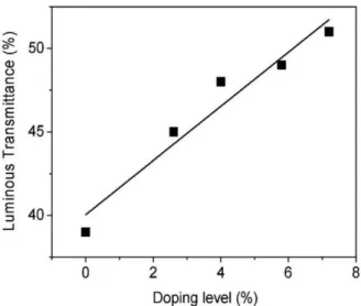
transition temperature as a function of W dopant in the VO2 film. Modified from [77]. ... 24
Figure 2.6 : Luminuous transmittance of MgxV1-xO2 films as a function of Mg doping
concentration. Reproduced with permission from [83]. ... 25 Figure 3.1 : Schematic of plasma sheath formation at the boundary. ... 31 Figure 3.2 : (a) Single collision (knock-out) and (b) Multiple collisions events happening during
sputtering. Modified from [93]. ... 32 Figure 3.3 Sputtering rate of SiO2 vs Ar+ ion energy. Reproduced with permission from [96] ... 33
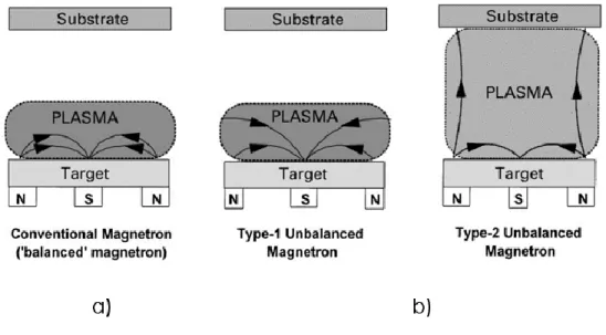
Figure 3.4 : Schematic of RF self-bias formation. Modified from [97] ... 34 Figure 3.5 : Schematic of plasma confinement in a DC magnetron sputtering discharge with (a)
balanced and (b) unbalanced magnetron configuration. Modified from [98]. ... 35 Figure 3.6 : In situ measurement of the optical properties of a Ti thin film after exposure to a plasma
of Ar:N2 measured in-situ ... 38
Figure 3.7 Equipotential contours for adsorption of argon on KCl. Modified from [119] ... 42 Figure 3.8 Potential energy distribution on (a) smooth surface, (b) around a step. Modified from
[119] ... 42 Figure 3.9 : The time variation of the number density of Pb nuclei deposited onto SiO2 substrates
for various temperatures; the data plots were obtained from electron micrographs. Reproduced with permission from [133]. ... 44 Figure 3.10 : Schematic representation of Volmer-Weber growth mode. The impinging atoms first
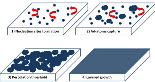
create nucleation sites (1) that gradually form nano-islands (2). As the thin film grows, the islands formation converges to the percolation threshold (3) and finally a thin film is obtained (4) ... 46
Figure 3.11 : Reflectivity of an undamped Drude metal as a function of frequency. For most metals, frequencies below 𝜔𝑝 include the near-infrared and frequencies above include the visible range. ... 52 Figure 3.12 : Spectral normal transmittance and near-normal reflectance measured for Ag films on
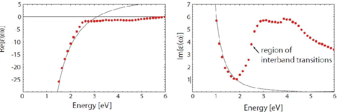
glass. The film thickness is denoted d. Modified from [147] ... 53 Figure 3.13 : Theoretical values (black lines) for 𝜀𝑟(𝜔)based on the Drude model and experimental
values (red lines) as a function of frequency. Reprinted with permission from [148] ... 53 Figure 3.14 : Two-dimensional film ... 55 Figure 5.1 : Schematic representation of the sample prepared for in-situ ellipsometry and
conductance measurements. The dimensions of the B270 substrate are 2.5 cm by 5 cm, and the distance between the electrodes is 1 cm. The multimeter is connected to the two aluminum electrodes. ... 73 Figure 5.2 : (a) Evolution of the three Stokes parameters S1 , S2 , and S3 for a wavelength of 1000
nm reflected off the sample during silver deposition on a B270 glass substrate. The first Stokes parameter S1 equals −1 after approximately 55 s of silver deposition due to the extinction of
the p-polarized light, as emphasized by the dashed line. (b) Evolution of the first Stokes parameter squared S12at multiple wavelengths. ... 75
Figure 5.3 : Deposition time at which the maximum of S12 is reached as a function of wavelength
with the addition of the fitted function. The solid line is the value for A in Eq. (5.15) (62.5) and represents an upper estimate for the value of the percolation threshold in seconds. ... 76 Figure 5.4 : (a) Measured current between two electrodes during silver film growth in semilog
scale. There are two different current evolutions before and after the transition point at 65 s (labeled I and II), indicating two different evolutions of the electrical properties due to different growth stages. (b) Measured current in normal scale. There is a rapid increase of current occurring right after 60 s of deposition. ... 78 Figure 5.5 : (a) Evolution of the first Stokes parameter squared S12 at multiple wavelengths on a
B270 glass substrate. The maximum value of S12 becomes stationary as a function of
wavelengths is defined as the percolation threshold. (b) Evolution of S12 at 500 and 1200 nm
for a continuous (cont.) and noncontinuous (n-cont.) deposition process. The distribution for the n-cont. deposition appears to be broader and shifted to a longer deposition time. ... 79 Figure 5.6 : Deposition time at which the maximum of S12 is reached as a function of wavelength
for a continuous deposition process. S12 reaches a maximum according to what seed layer is
beneath the silver layer. For example, the percolation threshold on a SiO2 layer occurs much
later in time than on the ZnSnO layer, due in part to the difference in surface energy between the two layers. ... 80 Figure 5.7 : (a) Ex situ sheet conductance measurements of silver for various continuous deposition
times on a logarithmic scale. The first measurement was possible after 51 s of deposition. The vertical dashed line indicates the percolation threshold time obtained by optical means. (b) Ex situ sheet conductance measurements of silver for various continuous deposition times on various surfaces. As expected from Table 5.3, the ZnO layer is more efficient at ... 82 Figure 6.1 : (a) High resolution XPS scan of the sulfur 2s orbital for the solution-processed
MPTMS SAM. The peak is centered at a sulfur-carbon binding energy of 228.1 eV (b) High resolution scan of the sulfur 2s orbital for the vapour-deposited MPTMS SAM. We notice the addition of the sulfates peak at 232.9 eV. ... 88 Figure 6.2 : (a) Atomic force microscopy images of a 7 nm silver film deposited on a MPTMS-treated borosilicate glass and (b) on a bare borosilicate glass sample. The average surface roughness (Rq) is shown (c) Optical characteristics obtained from ellipsometry measurements:
measured W for a 8.8 nm silver film on both the MPTMS-treated and untreated SiO2 surface. The sheet resistance values for the treated and untreated samples are shown ... 90 Figure 6.3 : High resolution XPS scan of the sulfur 2s orbital. The peak is centered at a sulfur-carbon binding energy of 228.1 eV. (b) High resolution scan after deposition of a sub-monolayer silver film. The peak is centered at a silver-sulfur binding energy of 226.6 eV. . 91 Figure 6.4 : (a) High resolution XPS scan of the sulfur 2s orbital for the MPTMS-treated SiN films
(b) High resolution scan after deposition of a sub-monolayer silver film. We notice the shift in energy from the top part due to binding to silver atoms. ... 93
Figure 6.5 Comparison of a simple design of a low-emissivity filter on a B270 glass substrate with and without MPTMS treatments. The sheet resistance values for both devices are shown. .. 94 Figure 7.1 : (a) In-situ ellipsometry during silver growth using magnetron sputtering on a glass
substrate. Optical properties change from an absorbing state (a dip in the spectra) to a fully reflective film. (b) Exposure of bare Ag film to reactive oxygen plasma. One can see the optical properties change within a few seconds as the film becomes oxidized. ... 100 Figure 7.2 : In-situ ellipsometry during exposure of a bi-layer of Ag (10nm)/Ti (2nm) film to a
reactive O2 plasma. (a) The Ti barrier thickness is sufficient to prevent degradation of the
silver film for low power plasma applied on the target (180 W). (b) The test is repeated with the plasma power on the target increased to 350W and the silver film eventually degrades. ... 102 Figure 7.3 : (a) Optical properties of a 3 nm Ti layer (b) Ti layer exposed to oxygen plasma for 300
seconds (c) Fully stoichiometric TiO2 layer. ... 103
Figure 7.4 : Sheet resistance of Ag/Ti bi-layer exposed to O2 plasma. There is an initial decrease
in the sheet resistance as the Ti barrier becomes oxidized. Eventually the exposure leads to degradation of the silver film. ... 104 Figure 7.5 : XPS survey data of Ag/Ti bi-layer before (a) and after (b) degradation with O2 plasma.
We see a great increase of the Ag atomic content on the surface after sample degradation accompanied by a decrease in Ti atomic content. ... 105 Figure 7.6 XPS survey data of degraded Ag/Ti sample (a) and subsequent in-situ sputtering of the
surface (b and c). There is a decrease in the Ag atomic content and an increase of the Ti atomic content following the gradual sputtering. ... 107 Figure 7.7 : TOF-SIMS scan on non-degraded (a) and degraded (b) Ag/Ti bi-layers. The interfaces
are well separated before degradation starts (a) and there is a strong intermixing after the degradation has occurred (b). Moreover we see in (b) that Ag and AgO species are present on the top interface. ... 109
Figure 7.8 : XPS survey data at grazing angle (70o) for SiO
2, ZnO and MPTMS underlayers. The
Ti2p peak is mostly visible for the MPTMS-tread SiO2 sample, due to a reduced amount of
Ag migrating to the surface. ... 110 Figure 8.1 Absorption spectra of Ag nanoparticles grown on borosilicate and capped with a layer
of ZnSnOx. The absorption red shifts and broadens as the particles grow. ... 115
Figure 8.2 : In-situ real-time ellipsometry of the oxidation process of a titanium barrier on Ag NPs. We see an initial broadening of Ψ after the deposition of the titanium barrier and a red-shift in the LSP absorption peak as the barrier is exposed to a reactive O2 plasma. After 2 minutes
of the oxidation process, the reactive O2 reaches the silver nanoparticles and the film loses the
characteristic LSP absorption. ... 117 Figure 8.3 : (Top) absorption spectra for different core-shell nanostructures obtained by oxidizing
and nitriding a sacrificial Si, Ti and Zn barrier (Bottom) Schematic of core-shell particle synthesis. Silver nanoislands are covered with a sacrificial layer (a) and exposed to a reactive plasma (b). ... 118 Figure 8.4 : Absorption spectra of silver NPs deposited at room temperature (RT) and at 300°C on
borosilicate glass and capped with a ZnSnOx layer. The absorption is narrower and greater
when the substrate is heated. ... 119 Figure 8.5 : Optical monitoring during deposition of silver. The minimum in the ellipsometry
variable Ψ is plotted as a function of deposition time. The dashed line represents the end of the deposition process. The optical monitoring past the deposition process shows a blue-shift in the LSP absorption for temperatures below 380 °C. ... 120 Figure 8.6 : 1 µm x 1 µm AFM images of nanoparticles on B270 glass deposited at room
temperature (a) and 380 °C (b). The histogram reveals a smaller base diameter, a smaller size distribution and greater height for the sample deposited at 380°C. ... 121
LIST OF SYMBOLS AND ABBREVIATIONS
List of abbreviations
AC Alternating Current
AFM Atomic Force microscopy
DC Direct Current
IEA The International Energy Agency MPTMS (3-Mercaptopropyl)trimethoxysilane
OECD Organisation for Economic Co-operation and Development PVD Physical Vapour Deposition
RF Radiofrequency
SF Solar Factor
SHGC Solar Heat Gain Coefficient
TOF-SIMS Time-Of-Flight Secondary Ion Mass Spectroscopy XPS X-ray photoelectron spectroscopy
Materials
Ag Silver
Ar Argon
Au Gold
AZO Aluminum doped zinc oxide BiOx Bismuth Oxide
H Hydrogen
ITO Tin-doped Indium Oxide
Li Lithium
N2 Nitrogen molecule
NbOx Niobium oxide
NiCr Nickel Chromium
O2 Oxygen molecule
SiN Silicon nitride
Ti Titanium
VO2 Vanadium dioxide
WO3 Tungsten oxide
Physical constants
𝜀0 Free space permittivity
𝜇0 Free space permeability
h Planck’s constant
𝑘𝐵 Boltzmann’s constant c Speed of light in vacuum
Symbols
𝛼 Spectral angular absorptivity
A Spectral absorbance
Asol Solar absorbance
𝐷65 Spectral distribution of illuminant D65
IB Spectral radiance of a blackbody
Isol Solar irradiance
𝑃𝑏 Planck distribution for blackbody radiation
Qamb Ambient radiative heat
Qem Re-emitted radiative heat
Qs Emitted thermal radiation from surface
R Spectral reflectance
Rsol Solar reflectance
𝑆𝑠𝑜𝑙 Spectral distribution of solar radiation at sea-level
T Spectral transmittance
Tc Critical temperature
𝑇𝑠𝑜𝑙 Solar transmittance 𝑇𝑣𝑖𝑠 Visible transmittance
LIST OF APPENDICES
Appendix A Transmission calculation coefficients ... 145 Appendix B List of publications ... 147
INTRODUCTION
Due to massive urbanization during the two previous centuries, the question of energy management can’t be dissociated from the energy consumption of residential and commercial buildings as the urban population density increases. Efforts towards research and technological developments for the purpose of reduced energy consumption in buildings are increasing on a global scale. One important development is the architectural glazing unit made of very thin optical layers to modulate the incoming solar radiation, allowing for significant reduction in the space heating or cooling energy consumption.
The use of thin film technology for energy saving is relatively new and has found tremendous success due to industrial scaling of effective coating methods and research interest in the wealth of possible applications inherent to the properties of thin films. However, this established, but yet open field, will require novel ideas to overcome the gap between today’s building energy management and the next generation of green, sustainable and even energy producing buildings. The doctoral project described in this thesis has been performed in collaboration with Guardian
Industries and includes scientific research pertaining to the design, fabrication and optimization of
low-emissivity (low-e) coatings performance using vapour phase deposition techniques. The present chapter will provide a brief overview of the problematics in the field of low-emissivity windows and the future trends that are to be expected in this field.
1.1 Problem definition
1.1.1 Worldwide energy consumption
The building sector accounts for approximately 35% of the world’s delivered energy consumption (among the industrial, transport and agriculture sectors) and for one-third of total energy-related CO2 emissions. With the ongoing urbanization of developing countries, the net energy consumption
of buildings (in the form of electricity and natural gas) is expected to increase by 32% until 2040 [1]. Thus, at the current rate, the energy consumption grows faster than the world’s population. A significant part of this consumption is related to the energy required to regulate the heat inside the building: cooling during summer in generally warm climates, and heating during winter or in generally cold climates.
Figure 1.1 : Final energy consumption by sector and buildings energy spread. From [2]. Figure 1.1 shows the energy consumption by sector for member countries of Organisation for Economic Co-operation and Development (OECD). We see that half of the energy demands of buildings is provided by electricity and natural gas. Therefore, a reduction in the global building energy consumption results in direct decrease of electricity usage as well as a reduction in the global CO2 emission. Moreover, as the world population continues to grow, we can expect these
numbers to increase as well. The International Energy Agency (IEA) is expecting the energy consumption related to space heating to increase by a total of 150% in developed countries and up to 600% in developing countries by 2050 [3].
The energy needed to heat or cool a building is dictated by the building envelope: This encompasses the roofing, wall, windows and foundations. An optimal building envelope must include proper sealing aimed for low air insulation, high reflective surfaces (in hot climate) such as white-coloured roof and high-performance windows with climate-appropriate solar heat gain coefficient (SHGC). It has been estimated that a high-performance building envelope necessitates only 20% of the average energy currently required to heat a building in a cold climate (for an OECD country member). In hot climates, the energy savings from reduced energy needs for cooling can go up to 40% [2]. The goal is to eventually reach the ‘energy-zero code’ building, where the yearly total consumption of the building amounts to the total energy gained from renewable energy sources stemming from the design and technologies utilized in the building; this includes even a positive
energy balance building which is not only self-sustainable but can also store and generate usable energy. Moreover, besides the need for new regulations for future building construction, it is estimated that up to 90% of the present infrastructures in the northern hemisphere will be operational in 2050 [4] and will necessitate modern renovations to meet new building code standard. Most building can last well over 100 years and the retrofitting can be costly; therefore, an appropriate design of the building envelope from the ground up is a vital requirement for long-term sustainability.
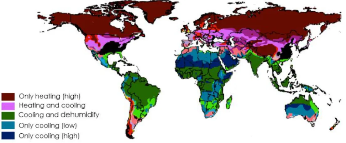
One of the key aspects of energy management in buildings resides in the glazing unit chosen for beneficial heat conservation or rejection by regulating the incoming solar radiation. The housing paradigm has shifted from residential buildings with a low glazing area to edifices with high glazing area, to benefit from increasing lighting comfort. Unfortunately, clear, untreated float glass is highly emissive and is responsible for solar radiative heat entering the building during the day in hot climates and interior blackbody radiation leaving the building at night in cold climates, causing excess charges in cooling and heating requirements. Figure 1.2 shows the world map divided into regions of low, moderate and high demands of heating or cooling. The map is divided into 17 different zones according to the annual demand in heating and cooling. We see that a very large portion of the maps relies solely on only heating or only cooling building demands.
Figure 1.2: World map of different climate zones according to the energy demands for heating or cooling. Modified from [5].
By using low-emissivity glazing in specific regions, the building units can benefit from coating treatments that convert a highly emissive float glass to a functional, energy efficient window. The technologies required to achieve this feat are vacuum-based technologies and the mechanisms behind the energy savings of low-emissivity coatings are related to the physics of thin films. Passive, low-emissivity coatings carefully designed for filtering the incoming energy radiation can be applied on single, double or triple glazing units and provide significant energy savings. Figure 1.3a shows the incoming solar radiation at sea level. Approximately half of the total radiation is in the visible spectrum (380-780 nm) and the other half lies in the near-infrared. The main challenge of the low-emissivity glazing is to achieve a high level of comfort and aesthetics (by providing high transmission and neutral color) and at the same time filter the desired amount of infrared radiation.
The working principle of a low-emissivity stack is to filter the incoming radiation by reflection from a thin, conductive transparent layer so that only a fraction of the total radiation is transmitted inside the building, as shown from the filled blue and green spectra in Figure 1.3a. In a hot climate, we want most of the solar radiation to be reflected outside by using a ‘low solar gain’ design. In a cold climate, we want a good portion of the solar radiation to be transmitted inside, while preventing the ambient blackbody radiation to escape at night, by using a ‘high solar gain’ design. Energy savings using this approach can be substantial over time. The US National Research Council estimated that low-emissivity glazing units were responsible for 1.79 trillion kW●h of cumulative savings in residential heating energy consumption from 1983 to 2005, which amounts to $37 billion (in 2003 dollars) in direct energy cost savings. The complete architecture of a low-emissivity device includes a very thin silver film (of the order of 8 to 10 nm) encapsulated by various metal-oxides to obtain the highest performance. Figure 1.3b shows a typical design for a low-emissivity coating, where a thin, infrared heat reflective silver layer is encapsulated between two transparent thin films. The blocking layer prevents ionic diffusion from the float glass production line into the layers. The seed layer helps the growth of the silver film, which acts as a passive heat reflector.
Figure 1.3: (a) Transmission spectra of high and low solar gain low-emissivity coatings against the incoming solar radiation at sea level (b) low-emissivity stack
The protective layer prevents damage made to the silver layer during the deposition process where reactive species generated inside the deposition chamber can corrode the silver film. Finally, the antireflective coating increases the visible transmission by reducing the reflection from the coated side using optical interference. This architecture acts as a guideline for a low-emissivity design but can be altered to bring additional functionalities (such as self-cleaning and resistance to erosion) of the glazing unit. The fundamental aspect of the thin-film stack is to maintain high visible transparency while lowering the overall emissivity. In that regard, reducing the silver film thickness while maintaining excellent electrical properties could not only achieve better optical properties but provide substantial economic savings (even a 10% reduction in silver film thickness can be sizeable when scaled over hundreds of millions of square meters.)
1.1.2 Silver growth and percolation
The use of silver at the nanoscale has extended over recent years to the development of applications such as low-emissivity windows [6, 7], transparent conductive electrodes (TCEs) [8-10], photovoltaics [11, 12], and studies on subwavelength confinement of light [13-15]. The extremely small scale at which silver films (or nanoparticles) are optically and electrically active makes the devices’ overall performance highly dependent on the choice of substrate and underlayer, surface
treatment, and growth mechanisms [16-19]. The growth mechanism during the deposition of silver and other transition metals on oxide surfaces has been explained as a surface diffusion, nucleation, and coalescence process in which the initial nucleation sites form and expand to nanoclusters (or nano-islands) by ad-atom capture, while subsequently forming a thin continuous film [20, 21]. The properties of the silver layers are expected to be very different at the various stages of growth as also reflected by the wide variety of applications based on silver on the nanoscale. The agglomeration of silver particles or clusters on the surface can be seen as a localized concentration of free electrons, which absorb incoming electromagnetic radiation. As aggregates expand, they connect to neighbouring clusters to eventually form a continuous film, a transition labeled the percolation threshold. This transition also marks the evolution between separated nanoclusters into a continuous, conductive film with heat-reflecting properties.
Various strategies have been employed eliminate cluster formation by modifying the surface beneath the silver film (the ‘seed’ layer). For example, a sub-nanometer Cu or Ge layer can provide nucleation sites for silver atoms, reducing their diffusion time on the surface which lead to the formation of a smooth silver film by suppressing nanoclusters formation [22]. Similarly, using a high-surface energy transparent film such as ZnO or PEDOT:PSS [23] one can inhibit the diffusion of evaporated silver atoms and produce thin, continuous films. Figure 1.4 shows the effect of a sub-nanometer Ge film on the silver growth. With the Ge seed layer, we obtain a continuous silver film whereas without the Ge layer we have separated nanoclusters for the same amount of deposited silver material.
Figure 1.4: Comparison between a 6 nm silver layer with (a) and without (b) a Ge wetting layer. Reprinted with permission from [22]
Similarly, a sub-nanometer Nb helps with early percolation and surface roughness reduction of silver films. Fig. 1.5 shows a 25 nm Ag film deposited on a TiO2 and Nb-coated (0.1 nm nominal
thickness) TiO2.
Figure 1.5: AFM pictures (1 µm ×1 µm) of a 25 nm Ag layer deposited without Nb (top) and 0.1 nm Nb on TiO2 (bottom). Reprinted with permission from [24].
The concept of metal-seeding has been extended to various elements such as Ti, Ni, Cr, Ta and Mo [24]. In some extreme case, the percolation threshold of a Au layer has been reduced to 1 nm using a sub-nanometer Cu seed layer [25]. The pre-inclusions of these metals cover the otherwise uniform oxide surface with nucleation sites that stop the diffusion of silver atoms through preferential binding. Nucleation of Ag on these metal seeds and subsequent thin film formation may be seen thermodynamically as a minimization of the surface free energy. If the interfacial free energy γint
(between the metal adatom and the substrate) is larger than the free surface energy mismatch between the bare substrate γsub and bare metal γm free surface energy, then island growth is
favoured. In other words, if Δγ = γm + γint – γsub > 0, island formation is favoured and for Δγ < 0,
wetting of the metal layer occurs [24, 26]. In other words, a substrate with free surface energy similar (or higher) than the deposited adatom will decrease the residual free surface energy Δγ and a layer-by-layer growth is initiated [27].
To understand the phenomena inherent to Ag growth, one can also use percolation theory. In this description, an arbitrary number of sites on a square lattice (or substrate) have a probability p of being occupied and a probability 1-p to be unoccupied, as shown in Fig. 1.6. In case of a conductive material, unoccupied sites represent insulating regions whereas occupied sites represent conductive regions. The growth of aggregates is not favourable to the formation of smooth, transparent conductive films and therefore we want to minimize the transition between separated clusters to a conductive film. Low melting point metals such as silver, gold and copper tend to have high diffusion coefficient when they are evaporated on a dielectric surface, owing to their high mobility. In the percolation theory picture, one way of reaching the critical density is to increase the probability p for each site by limiting atomic diffusion on the surface.
Figure 1.6: Probabilistic percolation theory. Each site on the square lattice has a probability p to be occupied. The filled dots represent discontinued clusters while the empty dots represent
continuity from one edge of the lattice to another. Reproduced with permission from [28]. The critical density of nucleation points is reached when there is a continuous path from one side of the substrate to the other. This moment is labeled the critical density and represent the transition between a dielectric and a conductive layer with a finite filling probability pc is associated with this
transition. Many physical properties of a metallic film such as their optical and physical properties can be linked to percolation. Since surface conductivity occurs at the percolation threshold, for p >
pc the d.c. conductivity σdc is proportional to |𝑝 − 𝑝𝑐|𝑢, where u is a constant based only on the
dimension of the lattice (substrate). For a two-dimensional film, u is equal to 1.30 and 1.99 for three-dimensional systems [28, 29]. Since surface filling probability p is linked to the film nominal thickness, we can state that σ𝑑𝑐 ∝ |𝑑 − 𝑑𝑐|1.3 for a two-dimensional thin silver film, for film
thickness d greater than the percolation thickness dc [28].
1.1.3 Silver degradation and the Kirkendall effect
Like other transition metals in the periodic table, silver physical properties (conductivity, ductility and electronegativity) are caused by its electronic configuration ([Kr]4d105s1) characterized by a
single electron in the 5s orbital and an unfilled d-orbital in its ionic form (Ag2+). This particular electronic configuration makes silver widely used as catalyst in many applications, and at the same time susceptible to form compounds that can potentially lead to the degradation of the film. The various degradation routes of silver have been reported as thermal decomposition, oxidation and atmospheric degradation. Silver degradation in ambient conditions is due mainly to the formation of silver sulfide (Ag2S) and silver chloride (AgCl), as well as carbonate compounds (Ag2CO3).
Oxidation of silver, however, does not occur in ambient conditions (even at high temperatures). A thin oxygen adsorbate layer can form on the silver layer, but no direct reaction with oxygen will occur. To form oxide compounds (Ag2O2, AgO, Ag2O), atomic oxygen or oxygen ions found in
low-earth orbit or deposition chambers, for example, are required.
When exposed to reactive oxygen, silver oxides will initially nucleate on the exposed silver surface. Due to a different diffusion coefficient between silver oxide outer layer and silver ions, the mobile Ag ions will start migrating outwardly through the oxide shell. The two materials (the silver oxide barrier and the silver layer) will migrate at a different rate. This different rate of diffusion will generate voids to compensate for the silver ions migrating outward, adding porosity to the material. Figure 1.6 shows an example of Ag nanowire exposed to an oxygen plasma. We can see that the exposure of the nanowires to the reactive oxygen generates increased porosity over time. This increase in porosity in the silver film in addition to the oxidation will drastically decrease silver film performance. The migration of two different materials through the interface separating them
and void generation has been known as the Kirkendall effect and has been exploited to create exotic nanostructures [30].
Figure 1.7: Ag nanowires (175 nm diameter) exposed to air plasma. Scale bar: 100 nm. Reprinted with permission from [31].
The Kirkendall effect is not only restricted to nanostructures such as nanoparticles or nanowires but can also occur for a planar configuration (dielectric/metal/dielectric). Figure 1.7 shows the interfaces between a silver film and TiO2 layers before and after exposure to an oxygen plasma.
Figure 1.8: TiO2 (20 nm)/Silver (14 nm)/TiO2 (20 nm) film degradation following exposure to
oxygen plasma. We see a clear interface separating the layers before the oxidation and interface mixing after the degradation. Reprinted with permission from [32]
Therefore, to obtain durable low-e coatings, we must control the growth of silver in order to get a rapid transition into the percolation threshold to obtain a smooth, continuous layer and protect the silver film from reactive oxygen.
1.2 Objectives
The central objective of this thesis is to optimize silver thin film properties by exploring new ways to obtain the thinnest possible continuous silver layers while maintaining their optical and electrical performances. By working on a set of novel monitoring tools and hybrid fabrication steps, we seek to obtain high performance and durable low-emissivity coatings that could help to cover the technological gap between today’s building design and high-performance envelopes. To achieve our central objective, this thesis present four sub-objectives, stated as follows:
1. Develop real time, in situ optical monitoring tools to understand the impact of deposition parameters on the evolution of the growth of metallic films on the nanoscale and detect the percolation threshold by using an all optical method.
2. Investigate thin silver films properties with improved heat rejecting performances by combining chemical surface modification and vapour deposition techniques.
3. Use surface treatment to prevent silver thin film degradation by atomic migration through the protective layers and void propagation caused by reactive oxygen during plasma-based process. 4. Develop optically dense and tunable plasmonic core-shell metallic nanostructures with industrial vapour deposition techniques for use in tinted, glare reducing and optically selective coatings.
1.3 Outline
The thesis is divided into 9 chapters, starting with the present chapter. In chapter 2 we will give an overview of the state-of-the-art energy saving thin film technologies, with a focus on current progresses and avenues in low-emissivity thin film stacks. Chapter 3 lays down the theoretical background for thin film deposition and growth in plasma-based processes. Chapter 4 reviews the experimental apparatus used to obtain the results presented in the thesis. Chapters 5 to 8 are the core results of this thesis. In chapter 5 we present a novel method to monitor silver thin film growth by measuring Stoke’s parameters in real-time. We show how to determine the percolation threshold of thin silver films using this method and test the growth of silver on different substrates. In chapter 6 we combine physical vapour deposition and chemical surface treatment to produce a high-quality, minimalistic SiN/Ag/SiN low-e architecture and demonstrate that a non-wetting surface can be
converted to a wetting layer using this treatment. In chapter 7 we investigate the degradation mechanism of silver in the presence of reactive oxygen and we present a solution on how to protect against this degradation. We observe that the deterioration process is akin to the nanoscale Kirkendall effect, where silver ions migrate towards the flux of diffusive oxygen within the thin film stack, even in the presence of a metallic barrier. In chapter 8 we demonstrate the fabrication of tunable core-shell nanoparticles deposited by magnetron sputtering using in-situ oxidation in a plasma. Moreover, we study the effect of temperature on the nano-islands distribution using in-situ ellipsometry to enable the fabrication of tunable solar-spectre selecting coatings. Finally, in chapter 9 we give a general discussion and outline the perspectives of the impact of our work on this field.
LOW-EMISSIVITY WINDOWS
2.1 Historical development
The use of thin silver films (with nanoscale dimensions) as a heat-reflective element can be dated back to 1916 with the invention of a ‘transparent screen’ mask for foundry furnace workers [33]. The function of this mask was to protect the workers from
“[…] the action of the ultra-violet rays at one end of the spectrum, and the infra-red or heat rays at the other end, for the eye is not injured by the mid-spectrum white light of moderate intensity.”
The prototype mask was designed to have a glass substrate coated using cathodic arc deposition with a thin metallic film (copper, gold, tungsten or nickel) and joined to a secondary slab of glass using a transparent resin, in order to protect the thin metallic film from mechanical degradation. The theoretical framework for this heat-rejecting effect was developed based on the well known effect that the reflectivity 𝑅 of a conductor at a certain electromagnetic frequency 𝜔 is related to its direct current (DC) conductivity 𝜎 through the Hagen-Rubens relation [34]:
𝑅 = 1 − 4√𝜔𝜋𝜀0 𝜎
(2.1)
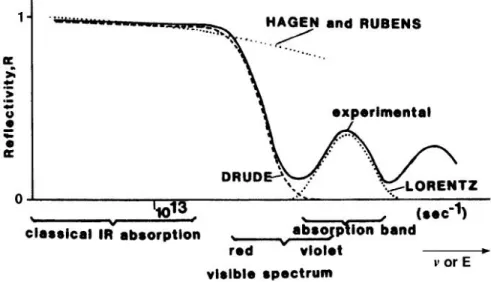
where 𝜀0 is the free space permittivity. For electromagnetic frequencies lower than the mid-infrared, the above relation holds well (Figure 2.1). As the frequencies increase to near-infrared and the visible range, other phenomena govern the optical response of the material (as we will see in Chapter 3).
Figure 2.1 : Schematic frequency dependence of the reflectivity of metals, experimentally (solid line) and according to three models. Reproduced with permission from [35].
Similarly, the study of radiative emission from a heated object and the relation between the radiation emitted by an object relative to the amount of radiation absorbed dates back to the 19th century; it can be well understood through the Kirchhoff’s radiation law [36]:
𝜀(𝜃, 𝜆) = 𝛼(𝜃, 𝜆) (2.2)
stating that at thermal equilibrium, the spectral angular emissivity 𝜀(𝜃, 𝜆) over a hemisphere above the surface area and electromagnetic wavelength 𝜆, is equal to the spectral angular absorptivity 𝛼(𝜃, 𝜆), and that a low absorbing medium (such as a highly reflective surface) would also demonstrate low emissive properties. The emissivity is a crucial parameter to determine Qs,
the emitted thermal radiation from the sample at a specific temperature T, given by [36, 37]
𝑄𝑠(𝑇) = ∫ 𝑑Ω𝑠cos 𝜃 ∫ 𝑑𝜆𝐼𝐵(𝑇, 𝜆)𝜀(𝜃, 𝜆) ∞ 0 (2.3) where ∫ 𝑑Ω𝑠 = ∫ 𝑑𝜃 sin 𝜃 𝜋 2 ⁄ 0 ∫ 𝑑𝜑 2𝜋
0 is an integral over the hemisphere above the emitter with the
azimuthal angle φ and polar angle θ. The spectral radiance of a blackbody 𝐼𝐵 at a specific temperature T is given by
𝐼𝐵(𝑇, 𝜆) =2ℎ𝑐 2 𝜆5 [𝑒 ℎ𝑐 (𝜆𝑘𝐵𝑇) ⁄ − 1] (2.4)
Where h is the Planck’s constant, c the speed of light in vacuum and kb Boltzmann’s constant.
It was only in 1937 that the first patent for a heat-reflecting roller-blind was issued for the specific use for energy saving in a residential building [38]. The invention prescribed the use of a thin silver film to filter out the infrared portion of the light and to transmit only the visible portion. However, no companies at the time saw the potential of these heat-reflecting devices, nor was there an incentive for replacing clear glass as fenestration units.
Throughout the following decades, major advances in coating technologies enabled the study of thin gold (Au) films embedded in bismuth oxides (BiOx) films. The BiOx films were deposited by
alternating current (AC) sputtering and the gold film by thermal evaporation. It was promptly observed that gold films deposited on BiOx seed layers had much better quality than when
deposited directly on glass [39], and that the transmission of a BiOx/Au/BiOx system was higher
than with a single Au layer alone. These two concepts, namely the improvement of the thin metallic film quality through the underlayer (seed layer) and the increase of the visible transmission by induced transmission are still some of the main research focus of low-emissivity coatings.
The energy crisis of 1973 was a serious incentive to revise the energy policy for countries that were heavily dependent on oil. During the crisis, the price of oil and coal nearly quadrupled [40], which had a significant impact on buildings that were relying on heating oil for furnaces and coal for electricity. From that point on, numerous companies tried marketing low-emissivity windows as a solution to reducing the costs of heating and cooling inside buildings. The first one was the German company FLACHGLAS, in 1975. They first tried silver as the reflecting layer but due to various problems went back to gold layers [41]. Moreover, the gold layer embedded in BiOx films gave a
green tint in transmission, that was deemed too unpleasant by the market which was still relying on air-insulated panes using only clear glass. The next challenge was therefore to find a color-neutral low-emissivity stack. The solution was found in the 1980s when it was demonstrated that silver (Ag), rather than gold, embedded in an asymmetrical configuration (that is, dielectrics of different thicknesses) could achieve the same infrared heat rejecting performance while possessing color neutrality [41, 42]. The first proposed stack was SnO2/Ag/NiCr/SnO2 coated on glass. The
nickel-chromium (NiCr) layer was introduced as a sacrificial layer which is essential to protect the Ag film from oxidation during the deposition process. Reaching this color-neutral, high transmittance low-emissivity coating was a milestone in the glazing industry and set the trend for the subsequent decades. Since then, more than 100 in-line magnetron coaters are operated worldwide to produce more than 500 million square-meters of coated low-emissivity glass every year.
Since the shift from gold to silver and the use of an asymmetrical design of the low-e coatings, challenges other than color neutrality are still present. Among these challenges we can mention long-term durability of the stack, the degradation of silver during the deposition process, the effect of heat on the mechanical and optical properties of the films in tempered glass, angular selectivity of double and triple silver coatings, inhibiting island growth during silver deposition to obtain ultra-thin continuous silver films, and many more. Nevertheless, silver-based low-emissivity glazing are still the most widespread technology for energy saving as they offer performance and reliability that other emerging or established technologies do not yet possess.
2.2 Solar Heat Control Coatings
As we have previously mentioned, the principal function of a low-e stack is to transmit a high portion of the visible spectrum while rejecting the near-infrared radiation. It can be thought of as a high-pass filter where the cut-off frequency is determined by the plasma frequency of the thin metallic film and the thicknesses of the dielectric layers. The amount of solar radiation transmitted through the glass, 𝑇𝑠𝑜𝑙(𝜃, 𝜆) can be expressed by [43]:
𝑇𝑠𝑜𝑙(𝜃, 𝜆) = ∫𝜆=3002500 𝑇(𝜃, 𝜆)𝑆𝑠𝑜𝑙(𝜃, 𝜆) 𝑑𝜆 ∫ 𝑆𝑠𝑜𝑙(𝜃, 𝜆) 𝑑𝜆 2500 𝜆=300 (2.3)
where 𝑇(𝜃, 𝜆) is the spectral transmittance and 𝑆𝑠𝑜𝑙(𝜃, 𝜆) the spectral distribution of solar radiation at sea level. The 𝑇𝑠𝑜𝑙 can be as low as 0.14 for a single layer silver, 0.11 for a double-silver coating, and 0.03 for a triple-silver coating [44]. These coatings can provide substantial energy saving compared to simple float glass which has a 𝑇𝑠𝑜𝑙 value of 0.85. Float glass is highly absorbent in the
infrared region above 4 µm and therefore highly emissive in the same region. Therefore, most of the absorbed radiation (both from the incident solar and room ambient radiation) inside the glass
is re-emitted equally in all direction. We saw in eq.2.3 how 𝜀(𝜆, 𝑇) was necessary to calculate the radiative heat emitted from a surface. The emissivity can be obtained using the following equation:
𝜀(𝜆, 𝑇) = 1 −∫ 𝑅(𝜆)𝑃𝑏(𝜆, 𝑇𝑏)𝑑𝜆 ∞ 0 ∫ 𝑃𝑏(𝜆, 𝑇) ∞ 0 𝑑𝜆 (2.4)
where 𝑅(𝜆) is the reflectivity and 𝑃𝑏(𝜆, 𝑇𝑏) is the Planck’ distribution for blackbody radiation at temperature Tb, given by [45]:
𝑃𝑏(𝜆, 𝑇𝑏) =
8𝜋ℎ𝑐
𝜆5(𝑒ℎ𝑐⁄(𝜆𝑘𝐵𝑇𝑏)− 1)
(2.5)
The emissivity of soda lime glass has been measured to be 0.87 [46] and that of a silver film to be 0.02 [47]. In addition to the solar heat directly transmitted through the window, the ambient temperature inside the room also plays a role in the heating energy balance by radiating in the mid-infrared (with the blackbody radiation distribution centered at 9 µm at room-temperature). The glass substrate is highly absorbing at those wavelengths and therefore it is highly emissive in that region. We saw from Kirchhoff’s law (eq.2.2) that a body at thermal equilibrium will radiate an amount of energy that it has absorbed. Since the absorption is isotropic, the re-emitted radiation is equal in every direction. However, the silver layer that prevents a portion of the near-infrared to be transmitted inside the room from the outside will also prevent the ambient heat to leave the interior by fully reflecting it back inside.
The metric for the performance assessment for energy saving is the Solar Heat Gain Coefficient (SHGC), also known as the Solar Factor (SF), given by [48]:
𝑆𝐻𝐺𝐶(𝜃, 𝜆) = 𝑇𝑠𝑜𝑙(𝜃, 𝜆) + ∑ 𝐹𝑖∙ 𝛼(𝜃, 𝜆)𝑖
𝑖
(2.6)
where F is a fraction of the heat re-emitted inside the room and 𝛼(𝜃, 𝜆), the solar absorption of the coated glass. This absorbed emission is re-radiated in all directions, but due to geometrical factors and possible thin film interactions, only a fraction of the light reaches the interior. This fraction of re-emitted light (𝐹 in eq. 2.6) has been evaluated to 0.46 for a silver-coated glass pane [49]. In presence of multiple glazing units, the expression 𝐹𝑖 ∙ 𝛼(𝜃, 𝜆)𝑖 is summed over all glass panes. The
𝑆𝐻𝐺𝐶 value can be as low as 0.42 for a single layer silver, 0.18 for a double-silver coating, and 0.11 for a triple-silver coating [44].
This heat-trapping effect is beneficial in colder regions where we would aim for a higher SHGC to let more solar radiation throughout the day and benefit from the heat-trapping during the night. In warmer climates, a glazing unit with a low SHGC is preferred to limit the amount of solar radiation passing through the window during the day. However, even for a low SHGC, the heat trapping effect still occurs but the overall heat gain is greatly reduced compared to clear glass [50]. Like the solar transmittance, the visible transparency of a window pane is quantified through the Tvis
coefficient, given by
𝑇𝑣𝑖𝑠(𝜆) = ∫ 𝑇(𝜆)𝐷65(𝜆)𝑉𝑝ℎ(𝜆)∆𝜆
780 𝜆=380
∫𝜆=380780 𝐷65(𝜆)𝑉𝑝ℎ(𝜆)∆𝜆 (2.7) where 𝑇(𝜆) is the spectral transmittance, 𝐷65(𝜆) is the relative spectral distribution of illuminant
D65 (given in Appendix A.1), and 𝑉𝑝ℎ(𝜆) is the spectral luminous efficiency for photopic vision.
𝑇𝑣𝑖𝑠 for clear (uncoated) glass is 0.89, and for a low-emissivity coating it can be as high as 0.86, denoting that we are able to achieve the same levels of visual transparency using a low-emissivity coating.
Figure 2.2 shows a simplified schematic of the various interactions between the solar radiation and the subsequent radiative heating pathways for a coated pane. The incident solar radiation undergoes multiple partial transmission and reflection at the interface of each of the thin films and the glass substrate. The sum over all partially reflected light is denoted by Rsol. The solar radiation
transmitted through the coating is also transmitted through the glass substrate where a portion of near-infrared radiation is absorbed (Asol). The radiation transmitted through the glazing unit
(substrate + coating) is denoted by Tsol. The ambient radiative heat is denoted by Qamb and the
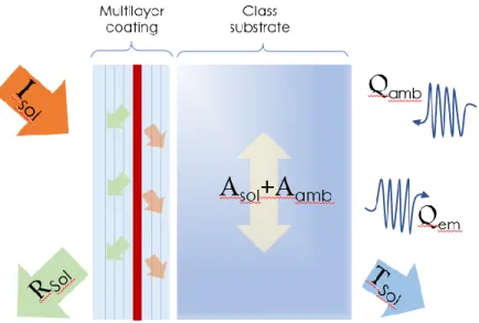
![Figure 2.4: Electrochromic device configuration. Reproduced with permission from [61]](https://thumb-eu.123doks.com/thumbv2/123doknet/2332361.32018/46.918.239.657.429.738/figure-electrochromic-device-configuration-reproduced-permission.webp)
![Figure 3.3 Sputtering rate of SiO 2 vs Ar+ ion energy. Reproduced with permission from [96]](https://thumb-eu.123doks.com/thumbv2/123doknet/2332361.32018/58.918.237.680.136.436/figure-sputtering-rate-sio-ar-energy-reproduced-permission.webp)