UNIVERSITÉ DE MONTRÉAL
SOLUTION PROCESSABLE SEMICONDUCTOR THIN FILMS: CORRELATION BETWEEN MORPHOLOGICAL, STRUCTURAL, OPTICAL AND CHARGE TRANSPORT
PROPERTIES
DILEK ISIK
DÉPARTEMENT DE GÉNIE PHYSIQUE ÉCOLE POLYTECHNIQUE DE MONTRÉAL
THÈSE PRÉSENTÉE EN VUE DE L’OBTENTION DU DIPLÔME DE PHILOSOPHIÆ DOCTOR
(GÉNIE MÉTALLURGIQUE) MAI 2013
UNIVERSITÉ DE MONTRÉAL
ÉCOLE POLYTECHNIQUE DE MONTRÉAL
Cette thèse intitulée:
SOLUTION PROCESSABLE SEMICONDUCTOR THIN FILMS: CORRELATION BETWEEN MORPHOLOGICAL, STRUCTURAL, OPTICAL AND CHARGE TRANSPORT
PROPERTIES
présentée par: ISIK, Dilek
en vue de l’obtention du diplôme de : Philosophiæ Doctor a été dûment acceptée par le jury d’examen constitué de : M. PETER Yves-Alain, Dr. Sc., président
Mme SANTATO Clara, Ph.D., membre et directrice de recherche M. TURENNE Sylvain, Ph.D., membre et codirecteur de recherche M. KYMISSIS Ioannis, Ph.D., membre
DEDICATION
I dedicate this work to my mother and father, Sacide and Ali Osman, and my sisters, Işıl and Meltem, who supported me throughout my life and education. No word can express how much I love you and how much I appreciate you.
“Bilmezdim şarkıların bu kadar güzel, Kelimelerinse kifayetsiz olduğunu.”
ACKNOWLEDGEMENTS
During the past five years, I have had the opportunity to interact with many invaluable colleagues at École Polytechnique de Montréal and with collaborators from other universities. Along the way, I have had the chance to build strong relationships, which I believe will be carried into the future. The process of obtaining my Ph.D. degree in Canada was an exquisite and rewarding experience, which I believe not only contributed to my scientific background and adaptation to a multicultural environment but also helped me in improving my interpersonal relationship and my leadership skills. Having interacted with a large group of people I owe many “Thank you!” for all the support I have received.
This Ph.D. thesis would not have been possible without the guidance of my supervisor Prof. Clara Santato. During the past five years, she was always there for me as a mentor to ensure high quality in our research. I would especially like to thank her for helping me realize my dream towards obtaining my Ph.D. and become an independent researcher and a scientist. I cannot fail to mention that she was always there to lend an ear when I needed one. I have been lucky with all the opportunities given to me for improving and developing my scientific skills. I am also proud to be the first Ph.D. student in her work group, which made my Ph.D. journey more interesting.
I would like to thank Prof. Sylvain Turenne for agreeing to be my co-supervisor for the completion of my Ph.D. degree in the Metallurgical Engineering program and for all the help and support he gave me during the past five years.
I would like to thank Prof. Fabio Cicoira, for all the support he gave me during my Ph.D.. I will always remember his contributions to my research and in the preparation of my thesis.
I would like to acknowledge our collaborators from Prof. John Anthony’s and Prof. William Skene’s groups for their contributions in the presented work.
I have been extremely lucky to learn the basics of semiconductor physics from Prof. R. Masut. I am grateful to him for being so helpful to me when I was trying to enter into the world of semiconductors. Also, I would like to mention Professors Yves-Alain Peter, Gilles L’Esperance, Jean Paul Bailon and Oumarou Savadogo for sharing their knowledge with me through classes or discussions. Many thanks to Prof. Sebastian Francoeur and Gabriel
Éthier-Majcher for their collaboration in obtaining photoluminescence spectra with upconverting materials (article in preparation).
Three summer students who worked with me contributed to the research for this thesis: Philippe Lefebvre, Jonathan Pison and Alexandre Labine. I would like to thank them all for all their work and their friendship in the laboratory.
To Jonathan Pison and Mathieu Maisonneuve, thank you for all the discussions on scientific issues and finally for helping me with the French translations. Merci beaucoup, encore une fois!
I would like to thank Ali Reza Mesgar for his friendship and the intellectual discussions we had at school. His expertise in microfabrication processes helped me in the successful completion of my microfabrication project with ITO.
With the help and dedication of Jeremy Lerner I have became an independent user of the PARISS fluorescence hyperspectral imaging system, which permitted to collect a significant part of my research at Ecole Polytechnique.
There are many people I would like to acknowledge who were behind the scenes during my Ph.D.: Dr. Khalid Laaziri, Marie-Hélène Bernier, Patricia Moraille, Jacqueline Sanchez, Christophe Clément, Yves Drolet, Jean Paul Lévesque, Joël Bouchard and Yves Leblanc.
My dear group friends (2008-2013), thank you all for all the useful discussions during group meetings and for your collaborations in the laboratory. I thank to all my friends for the laughter they brought into my life at Ecole Polytechnique. I will always remember them with their warm hearts and big smiles.
The ITO patterning process performed during the Ph.D. was supported by the Canadian Microelectronics Corporation (CMC).
RÉSUMÉ
Cette thèse de doctorat est le résultat d’un travail de recherche multidisciplinaire réunissant divers concepts fondamentaux comme l'ingénierie et la caractérisation des couches minces, l'électrochimie ainsi que la physique des dispositifs à base de couches minces semiconductrices.
L’objet des expériences menées lors du travail de thèse porte sur les couches minces semi-conductrices et leurs interfaces avec des matériaux électroniques ou des couches diélectriques. Le but ultime de la thèse est de mettre en corrélation la morphologie, la structure cristalline et la structure électronique des couches minces, ainsi que leurs propriétés fonctionnelles, avec le fonctionnement des dispositifs électroniques de type transistors utilisant ces mêmes couches minces en tant que matériau actif. En outre, de nouvelles stratégies fondées sur des phénomènes ayant lieu aux interfaces électrolyte/couche mince semiconductrice ont été explorées afin de contrôler la conductivité électrique au sein des couches minces.
Trois principaux systèmes chimiques ont fait l'objet d’études approfondies durant cette thèse: deux types de semiconducteurs organiques (oligomère et polymères dérivés d’azométhine-thiophènes et dérivés solubles de pentacène) et un semi-conducteur métal-oxyde (le trioxyde de tungstène, WO3).
Dans le but d’explorer les propriétés morphologiques de couches minces à base de semiconducteurs organiques, les microscopies à force atomique et à fluorescence en mode hyperspectrale ont été employées. Grâce aux observations réalisées par ces techniques, des hypothèses de corrélation ont été formulées entre les caractéristiques morphologiques et les propriétés de transport des porteurs de charges au sein des couches minces. La diffraction par rayons X en configuration glancing angle (GIXRD, utilisant de la lumière de synchrotron) a été utilisée pour examiner la structure cristalline des couches mais aussi pour en apprendre plus sur l'organisation moléculaire au sein de ces dernières.
Pour les transistors en couches minces, une configuration de type bottom contact a été choisie. Les caractéristiques de transfert et de sortie ont été utilisées pour calculer la mobilité des porteurs de charges, le voltage de seuil du dispositif ainsi que le ratio ION/IOFF.
Afin de contribuer à l'exploration de stratégies innovantes pour l'électronique de basse puissance basée sur des couches minces semiconductrices déposées à partir de méthodes en solution, tout en tirant parti de l'expertise du groupe de recherche dans la synthèse du WO3, des
transistors en couches minces de WO3 utilisant un électrolyte en tant que gating medium ont été
explorés durant ce travail de thèse. Le concept à la base de la stratégie est la formation d’une double couche électrique à l’interface électrolyte/couche mince de WO3 suite à l’application d’un
voltage aux bornes de l’électrode de grille immergée dans l’électrolyte, en contact avec la couche mince. La capacité de la double couche électrique a été mesurée par spectroscopie d'impédance électrochimique afin de calculer la mobilité des porteurs de charge dans la couche mince de WO3.
L’ARTICLE 1 traite des propriétés de transport des porteurs de charge dans les couches minces à base de molécules organiques de type dérivé soluble de pentacène (préparé par le groupe de recherche du professeur John E. Anthony, de l’Université du Kentucky). Les résultats du GIXRD ont suggéré un arrangement moléculaire favorisant le transport des porteurs de charge entre les électrodes de drain et de source, principalement dû à l’interaction des orbitales π-π perpendiculaires au canal du transistor. Dans ce travail, des substrats de SiO2 traités à l’HMDS
ont été utilisés pour améliorer la capacité d’étalement des couches et pour limiter la densité des sites piégeant les porteurs de charge au niveau de l’interface couche mince/diélectrique. Ces résultats ont été confirmés par des mesures à l’AFM où une bonne couverture de la surface a été observée. La caractérisation des transistors a révélé un comportement des porteurs de charge de type ambipolaire (c’est à dire transport simultané de trous et d’électrons). L’ambipolarité des couches minces vient de la bonne correspondance entre la valeur du niveau de Fermi de l’or (électrodes de source et de drain) et les niveaux HOMO et LUMO du dérivé soluble du pentacène en étude.
Le travail discuté dans l’ARTICLE 2 concerne des matériaux organiques tels que le thiophèno-azométhines π-conjugués, sous forme d’oligomère et de polymère, ainsi que des matériaux analogues de type dérivé d’oligothiophène. Dans le premier cas, les matériaux utilisent l’agent de couplage azométhines (-N=C-) alors que dans le deuxième cas, ils utilisent un agent de couplage plus conventionnel, de type (-C=C-). L’effet de l’extension de la conjugaison sur les propriétés de transport des porteurs de charge a été étudié. Le point clé de ce travail a est que les matériaux utilisant le couplage de type azométhine induisent des propriétés de transport
électronique au sein du transistor en couche mince, et ce pour la première fois. La microscopie à force atomique couplée à celle de fluorescence en mode hyperspectrale a été utilisée pour examiner l’étalement aux échelles micrométrique et nanométrique des couches minces d'oligothiopheno-azométhines. La caractérisation des transistors a permis de conclure que les matériaux de type oligothiophèno-azométhine et l'oligothiophène se comportent comme des semiconducteurs de type p tandis que le polythiophèno-azométhine se comporte comme un semiconducteur de type ambipolaire. De plus, la mobilité des trous de l’oligothiophèno-azométhine calculée après traitement thermique est de trois ordres de grandeur au dessus de son analogue oligothiophène utilisant l’agent de couplage (-C=C-). Cette étude ouvre donc une nouvelle possibilité pour l'amélioration des semiconducteurs basés sur l’agent de couplage de type azométhine.
L’intérêt grandissant pour les liquides ioniques - sels fondus à température ambiante - provenant de leurs propriétés physiques remarquables telles que leur faible volatilité et leur non-inflammabilité, dans le contexte de l’ARTICLE 3 nous a mené à les choisir comme électrolytes pour le gating de transistors à base de couches minces de WO3. Les couches minces de trioxyde
de tungstène ont été déposées sur des électrodes préfabriquées d’ITO par gravure chimique. Les microscopies à balayage électronique et à force atomique ont révélé une structure nanocristalline interconnectée dans les couches minces de WO3. Les transistors en contact avec le
1-butyl-3-methyl imidazolium bis (trifluoro1-butyl-3-methylsulfonyl) imide [BMIM] [TFSI], 1-butyl-3-1-butyl-3-methyl imidazolium hexafluoro phosphate [BMIM] [PF6] et 1-ethyl-3-methyl imidazolium bis (trifluoromethylsulfonyl) imide [EMIM] [TFSI] ont montré un comportement semiconducteur de type n. La possibilité d’obtenir des transistors à base de WO3 apparait alors comme une
excellente opportunité de produire de manière simple des transistors ayant des voltages d’opération faibles (au dessous de 1 Volts).
ABSTRACT
This Ph.D. thesis is a result of multidisciplinary research bringing together fundamental concepts in thin film engineering, materials science, materials processing and characterization, electrochemistry, microfabrication, and device physics.
Experiments were conducted by tackling scientific problems in the field of thin films and interfaces, with the aim to correlate the morphology, crystalline structure, electronic structure of thin films with the functional properties of the films and the performances of electronic devices based thereon. Furthermore, novel strategies based on interfacial phenomena at electrolyte/thin film interfaces were explored and exploited to control the electrical conductivity of the thin films. Three main chemical systems were the object of the studies performed during this Ph.D., two types of organic semiconductors (azomethine-based oligomers and polymers and soluble pentacene derivatives) and one metal oxide semiconductor (tungsten trioxide, WO3).
To explore the morphological properties of the thin films, atomic force microscopy was employed. The morphological properties were further investigated by hyperspectral fluorescence microscopy and tentatively correlated to the charge transport properties of the films. X-ray diffraction (Grazing incidence XRD, GIXRD) was used to investigate the crystallinity of the film and the effect of the heat treatment on such crystallinity, as well as to understand the molecular arrangement of the organic molecules in the thin film.
The charge transport properties of the films were evaluated in thin film transistor configuration. For electrolyte gated thin film transistors, time dependent transient measurements were conducted, in parallel to more conventional transistor characterizations, to explore the specific effects played on the gating by the anion and cation constituting the electrolyte. The capacitances of the electrical double layers at the electrolyte/WO3 interface were obtained from
electrochemical impedance spectroscopy.
In the context of ARTICLE 1, thin film transistors based on soluble pentacene derivatives (prepared by the research group directed by Professor J. Anthony, at the University of Kentucky) were fabricated and characterized. GIXRD results performed on the thin films suggested a molecular arrangement favorable to charge transport in the source-drain direction, with the π-π
stacking direction perpendicular to the channel. In ARTICLE 1, HMDS-treated SiO2 substrates
were used, to improve the surface coverage and to limit charge trapping at the dielectric surface. AFM showed good film coverage. The transistors showed ambipolar characteristics, attributed to the good matching between Au electrode work function and highest occupied molecular orbital (HOMO) and lowest unoccupied molecular orbital (LUMO) of the pentacene derivative.
The work reported in ARTICLE 2 deals with π-conjugated thiopheno-azomethines (both in oligomer and polymer form) and oligothiophene analogues. In the former case, couplings in the polymer are based on azomethine (-N=C-) moieties whereas in the latter case they are based on more conventional protocols (-C=C-). The effect of the coupling protocols on the corresponding thin film transistors behavior was studied. The key conclusion of this study was that thiopheno-azomethines thin films can be effectively incorporated into organic transistors: thin films of oligothiopheno-azomethines and the oligothiophenes exhibit p-type behavior whereas thin films of polythiopheno-azomethine exhibit an ambipolar behavior. The hole mobility of the heat-treated thin films of oligothiopheno-azomethines was three orders of magnitude higher compared to its oligothiophene analogue. AFM, coupled with hyperspectral fluorescence imaging, were used to investigate the micro- and nano-scale surface coverage. For the oligothiopheno-azomethine we were able to quantitavely deduce the surface coverage.
To contribute to the exploration of innovative strategies for low power consuming solution based electronics and capitalizing on the expertise of the group in the synthesis of solution deposited WO3 films the electrolyte gating approach was explored in ARTICLE 3. Ionic
liquids, that are molten salts at room temperature, were employed as the electrolyte. Ionic liquids are attractive for their low volatility, non-flammability, ionic conductivity and thermal and electrochemical stability. Thin films of WO3 were deposited onto pre-patterned ITO substrates
(source-drain interelectrode distance, 1 mm) prepared by wet chemical etching. SEM and AFM showed an interconnected film nanostructure. Electrolyte gated WO3 thin film transistors making
use of butyl-3-methyl imidazolium bis(trifluoromethylsulfonyl)imide ([BMIM][TFSI]), 1-butyl-3-methyl imidazolium hexafluoro phosphate ([BMIM][PF6]), and 1-ethyl-3-methyl imidazolium bis(trifluoromethylsulfonyl)imide ([EMIM][TFSI]) showed an n-type transistor behavior. The possibility to obtain WO3 electrolyte gated transistors represents an opportunity to
fabricate electronic devices working at relatively low operating voltages (about 1 V) by using simple fabrication techniques.
TABLE OF CONTENTS
DEDICATION ... III ACKNOWLEDGEMENTS ... IV RÉSUMÉ ... VI ABSTRACT ... IX TABLE OF CONTENTS ... XII LIST OF TABLES ... XVI LIST OF FIGURES ... XVII LIST OF ABBREVIATIONS ... XXII
CHAPTER 1 INTRODUCTION ... 1
1.1 The interest and applications of large area electronic devices, solution processed ... 1
1.2 Solution deposition for large area thin film electronics ... 2
1.3 Objectives and organization of the thesis ... 3
CHAPTER 2 THEORETICAL BACKGROUND ... 5
2.1 Materials ... 5
2.1.1 Organic semiconductors ... 5
2.1.2 Tungsten trioxide ... 10
2.2 Analogies and differences between organic and inorganic semiconductors ... 11
2.3 Structure, components and operating mechanism of thin film transistors ... 12
2.3.1 Basic thin film transistor structure ... 12
2.3.3 Gate dielectric ... 15
2.3.4 Organic thin film transistor operation ... 17
2.3.5 Mechanism of electrolyte gating ... 18
2.3.6 Transistor figures of merit ... 18
CHAPTER 3 EXPERIMENTAL METHODS AND TECHNIQUES ... 21
3.1 Sample preparation ... 21
3.1.1 Organic thin film transistors: device structure ... 21
3.1.2 Electrolyte gated thin film transistors: device structure ... 22
3.1.3 Ionic liquids ... 22
3.1.4 Cleaning and surface modification of transistor substrates ... 24
3.1.5 Solution preparation ... 25
3.1.6 Thin film deposition: spin coating and post-treatment ... 26
3.2 Transistor characterization ... 26
3.3 Morphological, Structural and optical characterization of thin films ... 27
3.3.1 Powder and thin film X-Ray Diffraction (XRD) and Grazing Incidence X-ray Diffraction (GIXRD) ... 27
3.3.2 Atomic force microscopy (AFM) ... 28
3.3.3 Fluorescence hyperspectral imaging ... 29
3.3.4 Scanning Electron Microscopy (SEM) and Energy Dispersive X-Ray Spectrometer (EDS) 30 3.4 Electrochemical Impedance Spectroscopy (EIS) ... 31
CHAPTER 4 MOLECULAR AND THIN FILM ENGINEERING OF π-CONJUGATED
PENTACENE DERIVATIVES ... 33
4.1 π-conjugated pentacene derivatives: Effect of the functionalization and the processing conditions on the thin film transistor performance ... 34
4.2 ARTICLE 1: Ambipolar organic thin film transistors based on a soluble pentacene derivative ... 36
4.2.1 Abstract ... 37
4.2.2 Introduction ... 37
4.2.3 Experimental ... 38
4.2.4 Results and Discussion ... 39
4.2.5 Conclusions ... 43
Acknowledgments ... 43
4.3 Correlation of charge transport properties with morphological and photophysical characteristics of solution processed pentacene derivatives... 44
CHAPTER 5 CHARGE-CARRIER TRANSPORT IN THIN FILMS OF π-CONJUGATED THIOPHENO-AZOMETHINES ... 49
5.1 ARTICLE 2: Charge-Carrier Transport in Thin Films of π-Conjugated Thiopheno-Azomethines ... 50
5.1.1 Introduction ... 51
5.1.2 Experimental ... 53
5.1.3 Results and Discussion ... 58
5.1.4 Conclusions ... 70
CHAPTER 6 ELECTROLYTE-GATED TUNGSTEN TRIOXIDE THIN FILM
TRANSISTORS MAKING USE OF IMIDAZOLIUM-BASED IONIC LIQUIDS ... 76
6.1 ARTICLE 3: Electrolyte-Gated Tungsten Trioxide Thin Film Transistors making use of Imidazolium-based Ionic Liquids ... 77
6.1.1 Abstract ... 78
6.1.2 Introduction ... 78
6.1.3 Experimental ... 80
6.1.4 Results and Discussion ... 81
6.1.5 Conclusions ... 86
6.2 Microfabrication of ITO microelectrodes ... 91
CHAPTER 7 CONCLUSIONS, PERSPECTIVES AND GENERAL DISCUSSION ... 99
LIST OF TABLES
Table 2-1 Comparison of the physical, electrical and optical properties of c-Si, WO3 and organic
semiconductors ... 11 Table 2-2 Transistor parameters ... 20 Table 3-1 Transistor channel widths (W) and lengths (L) in organic thin film transistors
investigated in this work. ... 22 Table 3-2 Gate dielectric properties for organic thin film transistors investigated in this work. ... 22 Table 3-3 Properties of the ionic liquids used for the characterization of electrolyte gated
transistors. ... 23 Table 3-4 Summary of the solutions and preparation conditions for organic thin films investigated
in thin film transistor configuration. ... 25 Table 4-1 HOMO and LUMO level location with respect to vacuum level and optical band gap of
three soluble pentacene derivatives determined by cyclic voltammetry synthesized by the group of Prof. J. E. Anthony at the University of Kentucky. ... 44 Table 4-2 Mobilities of 2,3-CN2-TIPS-Pn, TIPS-F8 and TES-F8 as a function of temperature and
deposition solution concentrations. ... 46 Table 5-1 Electrochemical and photophysical properties of compounds 1-3. ... 61 Table 6-1 Process steps for photolithography and etching of ITO substrates. ... 93
LIST OF FIGURES
Figure 2-1 Conjugated backbone of pentacene molecule with alternating single and double bonds. ... 6 Figure 2-2 C2H4, bonds and orbitals, showing the delocalized electron regions forming the
π-bonding above and below the C atom plane. ... 6 Figure 2-3 Molecular energy structure of a conjugated molecule showing the bonding and anti-bonding orbitals. The gap between π-π* orbitals is the energy band gap of the molecule [71]. ... 7 Figure 2-4 Energy band diagrams for an ordered molecular crystal and a disordered molecular
material [71], [87], [88]. ... 7 Figure 2-5 Chart showing molecular weights of oligomers and polymers together with the degree
of polymerization. ... 8 Figure 2-6 Selected contributions in the molecular structure of an organic semiconductor that can
affect its chemical and physical properties, for the specific case of the 2-Amino-5-[(3,4-bis(decyl)-5-formylthiophen-2-ylmethylene)-amino]thiophene-3,4 dicarboxylic acid diethyl ester molecule investigated in this Ph.D. work (Chapter 5) ... 8 Figure 2-7 Molecular structure of (a) pentacene (insoluble) (b) 6,13-bis (triisopropyl-silylethynyl)
pentacene(TIPSpentacene,soluble),and(c)2,3dicyano6,13bis(triisopropylsilylethynyl)pentace ne (2,3-CN2-TIPS-Pn, soluble). ... 9 Figure 2-8 The effect of the substituent groups on the HOMO-LUMO energy levels of (a)
pentacene (Eg=2.29 eV) (b) 6,13-bis (triisopropyl-silylethynyl) pentacene (TIPS-pentacene,
Eg=1.81 eV) , and (c) 2,3-dicyano-6,13-bis-(triisopropylsilylethynyl)pentacene
(2,3-CN2-TIPS-Pn, Eg=1.81 eV). ... 10
Figure 2-9 Corner-sharing WO3 octohedra. ... 11
Figure 2-10 Thin film transistor configuration: (left) bottom gate/bottom contact and (right) bottom gate/top contact. W is the channel width and L is the channel length. ... 12
Figure 2-11 Scheme of the metal/p-type semiconductor interface. The hole (electron) injection barrier, Фh (Фe), is the difference between HOMO (LUMO) level of the organic
semiconductor and the Fermi level of the metal. Фh is small enough for hole injection. The
effect of an applied bias at the gate electrode on the HOMO and LUMO levels at the interface is also shown by a small bending. GDOS is also shown. (Adapted from [71]) ... 14 Figure 2-12 ITO/WO3 interface energy band diagram. The Фe for electron injection is <0.1eV. . 15
Figure 2-13 Schematic illustration of organic thin film transistor operation. Circles in the semiconductor layer illustrate the holes during different stages of transistor operation. In (a) Cut-off, (b) Linear region and (c) the saturation region are illustrated. ... 17 Figure 2-14 General structure of an electrolyte gated transistor (left). Electrochemical mechanism
(top right) and electrostatic mechanism (bottom-right) of doping during electrolyte gating. 19 Figure 3-1 Bottom contact-bottom gate (Si (n+)) transistor substrate with interdigitated pre-patterned Au electrodes (30 nm thick) and SiO2 (195 nm) gate dielectric coated with an
organic semiconductor. ... 21 Figure 3-2 Electrolyte gated transistor built on a glass substrate with patterned ITO electrodes.
The channel is in contact with the electrolyte, confined in a PDMS well on top of the channel. An electrode immersed into the electrolyte is used to gate the channel. ... 23 Figure 4-1 Molecular formulas of (a) triethylsilyl-octafluoropentacene, (b)
Bis(triisopropylsilylethynyl)octafluoropentaceneand(c)Bis(triisopropylsilylethynyl)dicyanop entacene………..………33 Figure 4-2 Molecular structure of 2,3-CN2-TIPS-Pn (a); bottom gate/bottom contact FET
structure used in this work (b); HOMO and LUMO levels of pentacene and 2,3-CN2-TIPS-Pn, with respect to the Au workfunction, Au (c).[100] ... 39
Figure 4-3 1 µm × 1 µm AFM topographical images of 2,3-CN2-TIPS-Pn film on HMDS-treated SiO2. Inset: 5 µm × 5 µm AFM image of the same sample, rms = 1.56 nm. ... 40
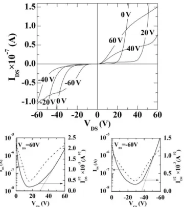
Figure 4-4 TFT characteristics of 2,3-CN2-TIPS-Pn films: output curves (Ids vs Vds) for |Vgs| = 0,
Vds = 60 V (bottom left); transfer curves at saturation for Vds = -60 V (bottom right).
Channel width/Channel Length = 10 µm/1880µm... 41 Figure 4-5 (a) Rietveld fit of one of the X-ray diffraction images collected at an incident angle of
2°. The principal spot is due to the (001) diffracting plane parallel to the sample surface. The bottom 2D pattern represents the experimental data; the recalculated pattern is on top. The three spots (001/002/003 reflections) are aligned in the diffraction plane normal to the sample surface. As we move out of it (moving vertically in the image), the strong texture causes a rapid decrease of the intensity. The inset reports the recalculated pole figure showing the strong 00l orientation (mrd: multiple of random distribution, values in log scale). (b) Proposed molecular arrangement of 2,3-CN2-TIPS-Pn on the substrate. ... 42 Figure 4-6 Absorption and fluorescence spectra (excitation wavelength 540 nm) of spin coated
thin films heat treated at 100 °C on quartz slides. ... 45 Figure 4-7 TFT characteristics of spin coated and 100 °C annealed TIPS-F8 and TES-F8 films:
output curves (Ids vs Vds) for |Vgs| = 0, 20, 40, 60 V (a) TES-F8 and (b) TIPS-F8; transfer
curves (sqrt Ids vs Vgs) at saturation for Vds = 60 V (c)TES-F8 and (d) TIPS-F8. Channel
widths/Channel Length = 6 µm/1880µm and 10 µm/1880µm for TES-F8 and TIP-F8, respectively. ... 47 Figure 4-8 1µm×1µm height and phase AFM images of the three molecules in the as-prepared
and 100 °C annealed conditions. ... 48 Figure 5-1. Cyclic voltammograms of 1 (black, bottom), 2 (red, middle) and 3 (blue, top)
recorded in de-aerated dichloromethane with TBAPF6 (0.1 M) using a saturated Ag/AgCl as
reference electrode and a Pt wire as both the working and auxiliary electrode. ... 61 Figure 5-2 Powder X-ray diffraction of 1 (black, bottom), 2 (blue, middle) and 3 (red, top). The
XRD powder data for 1 and 2 show diffraction peaks corresponding to a lamellar morphology (as per the inset sketch), consistent with π-stacking distance of 3.77 Å found from the single crystal data; the peak at 2 ≈ 4.2° corresponds to an interlayer d-spacing of 21.2 Å, represented in the sketch in the inset. ... 63
Figure 5-3 50 µm×50 µm fluorescence hyperspectral images of spin-coated films of 1-3 on HMDS-treated SiO2/Si FET substrates, after thermal treatment at 100 °C. Left:
corresponding categorized images for 1 (a, λexc = 540 nm), 2 (b, λexc= 540 nm), 3 (c, λexc =
460 nm), Right: Histograms and collected spectral libraries of 1 (d), 2 (e), 3 (f), respectively. ... 65 Figure 5-4 AFM images of thin films of 1-3 on HMDS-treated SiO2/Si FET substrates: (a) 5 µm
× 5 µm and (b) 20 µm × 20 µm images of as-prepared films of 1; H range = 0-80 nm, rq = 8-9 nm. (c) 5 µm×5 µm and (d) 20 µm × 20 µm images of 100 °C-treated films of 1; H range = 0-100 nm, rq = 12.4-13 nm (rq 0.9 nm in the underlayer, see text). (e) 5 µm × 5 µm image of 2 treated at 100 °C; H range = 0-15 nm, rq ~1 nm. (f) 5 µm × 5 µm image of 3 treated at 100 °C; H range = 0-500 (see text for a discussion on rq). (b) and (d) have been taken on the transistor channel (electrode patterning visible in the images). ... 67 Figure 5-5 Output (left) and transfer (right) curves for FETs based on thin films of 1 (top) and 3
(bottom). In the output curves, VGS were 0, -20, -40, -60 V. The transfer curves were
recorded at VDS = -60 V; the red line extrapolates the square root of IDS at its maximum
slope to obtain its intercept at y = 0, to calculate VTH. ... 69
Figure 6-1 Device structure of the electrolyte gated WO3 thin film transistor with the electrolyte
confined by a PDMS well, on top of the WO3 channel. The structures of the
imidazolium-based ionic liquids for this work are also indicated. ... 79 Figure 6-2 Output characteristics of EG WO3 transistors making use of ionic liquid electrolytes
(W/L = 1000 µm/6000 µm) with VGS increasing from 0 to 1 V with 0.2 V steps. (a)
[EMIM][TFSI] WO3 transistors. (b) [BMIM][PF6] WO3 transistors. In the output curves, the
hold time at a certain VGS (before the acquisition of the current versus VDS at a certain VGS)
is 600 sec. ... 83 Figure 6-3 Nyquist (a) and Bode (b) plots of two-electrode (WO3/IL/Pt) electrochemical cells
with [EMIM][TFSI] (EDC = -1V), [BMIM][TFSI] (EDC = -1 or -2V), [BMIM][PF6] (EDC =
-1V). (c) Capacitance versus EDC plots for the three electrochemical cells making use of the
Figure 6-4 Spin speed versus thickness curves for 4 inch Si-wafers spin coated with SPR 220 photoresists. The difference in the photoresist thickness for the Si wafer (red dashed line)
and the ITO substrate (blue dashed line) ... 92
Figure 6-5 Mask layouts used for ITO patterning. ... 93
Figure 6-6 ITO substrate ... 93
Figure 6-7 Photoresist coated ITO substrate, thickness ~2,75 µm ... 93
Figure 6-8 Hard contact (i-line, 365nm, exposure) ... 94
Figure 6-9 Patterned ITO glass ... 94
Figure 6-10 100 µm channel and developed 100 µm features of photoresist on ITO. Image taken under polarized light after 3 min 40 sec development, no photoresist was observed. ... 95
Figure 6-11 Developed photoresist cross section after 3 min 40 sec. Calibration correction 43% giving ~2.75 µm depth. ... 95
Figure 6-12 Optical images of step-by-step wet chemical etching. ... 96
Figure 6-13 SEM Images showing the fabricated (a) ITO electrodes, (b) 1000 µm channel. ... 97
Figure 6-14 A portion of the transistor substrate showing the chemical distribution of elements in and around the channel, as obtained from a EDX survey. After etching In and Sn are replaced by Si and O, i.e. ITO was etched and glass substrate was reached. ... 97
Figure 6-15 Spectra taken from different regions of the sample showing the presence of different elements in and near the transistor channel. These spectra clearly shows that no In or Sn residues were left in the channel after etching. ... 98
LIST OF ABBREVIATIONS
AFM Atomic force microscopy CB Conduction band
CV Cyclic Voltammetry
EDX Energy-dispersive X-ray spectroscopy EDL Electrical double layer
EG Electrolyte gated
EIS Electrochemical impedance spectrometry HOMO Highest occupied molecular level IL Ionic liquid
LUMO Lowest unoccupied molecular level OSC Organic semiconductor
SEM Scanning electron microscope TFT Thin film transistor
VB Valence band XRD X-Ray diffraction Фe electron injection barrier Фh hole injection barrier
CHAPTER 1
INTRODUCTION
The underpinning of the present Ph.D. work is the investigation of the relationship between the solution based processing conditions of thin semiconductor films and the performance of devices based thereon.
1.1 The interest and applications of large area electronic devices, solution
processed
Solution processed electronic devices are interesting for large area applications due to their low cost and compatibility with flexible substrates [1], [2], [3], [4], [5], compared to well established silicon based electronic devices [6].
Organic semiconductors and metal oxide semiconductors are the two classes of material groups that are commonly employed for solution processed large area device fabrication. Currently, semiconductor industry is dominated by silicon, with electron mobility (µe) ~
1000
cm2/V·sec inwell established devices and ~ 600 cm2/V·sec on plastic flexible substrates [7][8]. Amorphous silicon (a-Si) is widely used for high durability and relatively low mobility applications [9]. Organic semiconductors usually demonstrate electronic performances close to, and in some cases exceeding, that of a-Si. While the µe of a-Si thin film transistors (TFTs) was reported to be on the
order of 1 cm2/V·sec [10], hole mobility (µh) as high as 3.2 cm2/V·sec and µe as high as 2
cm2/V·sec for single crystal pentacene were reported [11] and µh 1.5 cm2/V·sec for thin films of
pentacene was reported [12]. A value of µe of 5.5 cm2/V·sec for a single crystal of perylene was
also reported [13].
Oxide semiconductor films yield mobility in the range 1-100 cm2/V·sec [9], [14], [15]. In-Ga-Zn-O system yielded high µe in TFTs on plastic substrates, of 6-9 cm2/V·sec [15].
While benchmark inorganic semiconductors can be operated at low operating voltages, this is not the case for many organic semiconductors, thus limiting the commercialization of organic electronic products, such as Radio Frequency Identification Devices (RFID) [16].
During the past decade, there has been an effort to tackle the high operating voltage issue by approaches based on replacing conventional gate dielectric such as SiO2 (ɛ=3.9) by high-k
materials such as Al2O3 and HfO2 (ɛ=10-15) and reducing the thickness of the dielectric layer by
the use of dielectric self-assembling monolayers [17], [18], [19, p. 2], [20]. An alternative approach is based on the concept of electrolyte gating, proven to reduce the operating voltages of transistors from dozens of volts to a few volts [21], [22], [23]. The first examples of electrolyte gating were proposed by Brattain et. Al [24]. Wrighton in the 1980s reported a number of electrolyte gated organic and inorganic transistors, thus preparing the basis for the advanced studies currently ongoing worldwide [25], [26], [27], [28], [29].
Application areas for organic electronics and oxide electronics can be listed as thin film transistors (TFTs) to be used in data storage, active matrix displays, flexible display devices [9], [30], [31], [32], RFID tags to replace barcodes [33], [34], [35, p. 56], solar cells [36], [37], [38], [39], gas-sensors and bio-sensors [25], [26], [40], [41], [42], [43], [44], [45], X-ray detectors [46] light-emitting diodes (LEDs) [47], [48], [49], [50], smart textiles (equipped with sensors, displays, solar cells and heaters) [51], [52], [53], e-paper [54].
1.2
Solution deposition for large area thin film electronics
Organic electronics stemmed from the discovery of conductive polymers by Alan J. Heeger, Alan G. MacDiarmid, and Hideki Shirakawa [55]. This discovery brought them the Nobel Prize in Chemistry in 2000 [56], [57], [58]. In the Nobel lecture, Alan J. Heeger summarized the discovery with these words: “Conducting polymers offered the promise of achieving a new generation of polymers: materials which exhibit the electrical and optical properties of metals or semiconductors and which retain the attractive mechanical properties and processing advantages of polymers”. Most organic semiconductors are indeed soluble in organic solvents such as chloroform, chlorobenzene, toluene and xylene.
Oxide semiconductors on the other hand, have been used in oxide thin films transistors since 1960s [59], [60], [61], [62], [63]. Semiconductor oxides can be prepared by the sol-gel technique, which is a solution based synthetic method [62], [64], [65], [66]. They are less prone, compared to organic semiconductors, to degradation upon contact with H2O or O2, such as they can be used
in contact with aqueous electrolytes for electrochromic and photoelectrochemical applications [67], [68], [69], [70, p. 3].
Manufacturing techniques i.e. roll-to-roll, doctor blade, inkjet printing and screen printing technologies allow production of electronic devices with dimensions from tens of micrometers to dimensions exceeding tens of meters [9], [71], [72], [73].
1.3 Objectives and organization of the thesis
The general objective of this thesis was to contribute to advance the knowledge in the field of structure-property relationships in semiconductor thin films deposited by solution based techniques with the aim to shed light on their functional properties and, afterwards, devices based thereon.
The research efforts whose results constitute this Ph.D. thesis work are multifaceted, indicated below as research efforts A-D.
A - Thin film engineering – In Chapters 4 and 5, we reported on new soluble organic materials (2,3-dicyano-6,13-bis-(triisopropylsilylethynyl)pentacene (2,3-CN2-TIPS-Pn), 2-amino-5-[(3,4-bis(decyl)-5-formylthiophen-2-ylmethylene)-amino]thiophene-3,4 dicarboxylic acid diethyl ester, thiopheno-polyazomethine and 2,5-Bis[(E)-2-(5-methylthiohene-2-yl)vinyl] thiophene) synthesized by organic chemists collaborators. We carried out systematic investigations on the thin film deposition conditions (substrate surface modification, solution concentration, solvent, thermal treatment conditions) to obtain homogeneous films with complete substrate surface coverage. We characterized the morphology of the organic thin films by atomic force microscopy and fluorescence hyperspectral imaging. The structure of the films was investigated by grazing incidence X-ray diffraction at the Elettra synchrotron facility (Trieste, Italy). In Chapter 6, the morphology and the structure of metal oxide solution processed thin films were followed by atomic force microscopy and scanning electron microscopy.
B - Microfabrication of transistor substrates hosting the thin films – The thin film engineering efforts were paralleled by the characterization of their charge carrier transport properties in thin film transistor configuration. The microfabrication of the transistor substrates
represents a relevant portion of the experimental efforts carried out within the context of this Ph.D. work (Chapter 6).
C – Characterization of the thin film transistors to study the electroactivity of the thin films, the polarity and the mobility of the charge carriers (Chapters 4, 5, 6). Device characterization was performed in controlled atmosphere conditions (vacuum 10-5 Torr or N2
glove box atmosphere with O2 and H2O at about 1 ppm).
D – Exploration of an unconventional transistor gating approach (electrolyte gating) with metal oxide films (Chapter 6). With the aim to lower the operating voltages of the transistors the electrolyte gating approach was employed, making use of imidazolium-based room temperature ionic liquids. The formation of an electrical double layer at the ionic liquid/thin film interface underpins the effectiveness of the gating.
CHAPTER 2
THEORETICAL BACKGROUND
In this chapter, a theoretical background on the properties of the materials used in the Ph.D. is given. In addition, analogies and differences between organic and inorganic semiconductors are listed in Table 2-1 to clarify where organic and oxide semiconductors stand in terms of electronic applications, with respect to Si. Moreover, since during this Ph.D. work the transistor configuration was selected as a test-bed to study the charge-transport properties of the materials, a general view of transistor operation and characterization is proposed.
2.1 Materials
2.1.1 Organic semiconductors
Organic semiconductors possess a conjugated backbone i.e. carbon atoms form alternating single and double bonds, such as in pentacene (Figure 2-1). In a conjugated system, each C atom has 3 nearest neighbors with whom it forms 3 equivalent σ bonds. The bonds are built using the sp2 hybridization of the three valence atomic orbitals of the carbon atom 2s, 2px and 2py. The
fourth orbital, 2pz, lies perpendicular to the plane of the σ bonds. The overlap of the two
out-of-plane 2pz atomic orbitals give π bonds [74], with a delocalized electron density above and below
the plane of the C atoms, as illustrated for the ethylene moleculein Figure 2-2 [75].
The difference in energy (Eg) between the bonding () and anti-bonding () molecular
orbitals are illustrated in Figure 2-3. The HOMO (Highest Occupied Molecular Orbital) and LUMO (Lowest Unoccupied Molecular Orbital) of organic semiconductors are analogous to valence (VB) and conduction band (CB) edges of inorganic semiconductors. In organic semiconductors, σ-bonds contribute to the stability of the molecular structure whereas π bonds enable charge transport.
Figure 2-1 Conjugated backbone of pentacene molecule with alternating single and double bonds.
Figure 2-2 C2H4, bonds and orbitals, showing the delocalized electron regions forming the
π-bonding above and below the C atom plane.
Because Van der Waals intermolecular interactions are weaker compared to covalent interactions, in molecular thin films the electronic wave function is strongly localized to individual molecules [76], [77]. The variable range hopping model, where charge carriers hop between adjacent molecules, is commonly accepted as the charge carrier transport mechanism in organic semiconductors with room temperature mobility below 10-2 cm2/V·sec [75], [78], [79], [80]. The fluctuations of the intermolecular spacings in organic semiconductors that lack long-range order lead to local variations of the wavefunction such that the HOMO and LUMO levels show an energetic distribution that can be approximated by a Gaussian density of states (GDOS). The difference in the DOS distribution between ordered molecular crystals and disordered organic materials is illustrated in Figure 2-4 [75], [81], [82]. There is also evidence of band-like transport for a number of organic semiconductors such as 6,13-bis(triisopropylsilylethynyl)-pentacene (TIPS-6,13-bis(triisopropylsilylethynyl)-pentacene) and 6,13-bis(triisopropylsilylethynyl)-pentacene [83], [84], [85], [86].
Figure 2-3 Molecular energy structure of a conjugated molecule showing the bonding and anti-bonding orbitals. The gap between π-π* orbitals is the energy band gap of the molecule [71].
Figure 2-4 Energy band diagrams for an ordered molecular crystal and a disordered molecular material [71], [87], [88].
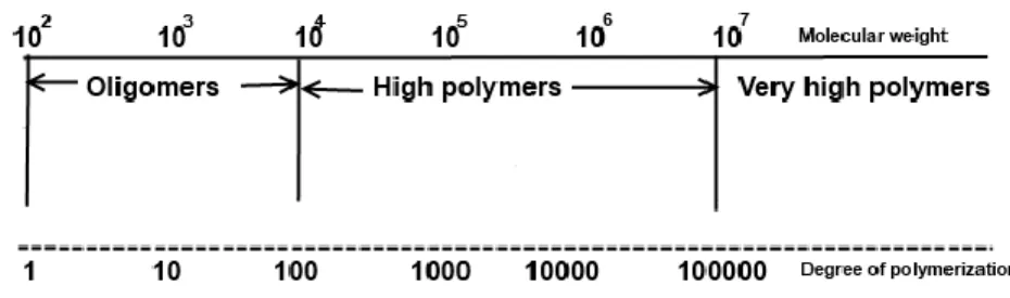
Organic semiconductors are found in the form of oligomers and polymers (Figure 2-5) [89]. Oligomers possess low-molecular weights that permit them to be vacuum-deposited. Conjugated polymers, on the other hand, have high-molecular weights and can be solution processed. The chemico-physical properties of organic semiconductor thin films are dramatically affected by molecular structure (Figure 2-6) as well as supramolecular arrangement in the film. Controlling the chemical structure through chemical synthesis and engineering the
supramolecular arrangement in the films can therefore promote specific, desirable functional properties in thin organic electronic films [90], [91], [92], [93], [94], [95].
Figure 2-5 Chart showing molecular weights of oligomers and polymers together with the degree of polymerization.
Figure 2-6 Selected contributions in the molecular structure of an organic semiconductor that can affect its chemical and physical properties, for the specific case of the 2-Amino-5-[(3,4-bis(decyl)-5-formylthiophen-2-ylmethylene)-amino]thiophene-3,4 dicarboxylic acid diethyl ester molecule investigated in this Ph.D. work (Chapter 5)
Acenes are a group of organic semiconductors that have been widely investigated [3]. Pentacene (Figure 2-7 a) and its derivative TIPS-pentacene (Figure 2-7 b) are two well-known acenes [3], [96]. The addition of specific substituents can influence the solubility of organic semiconductors such that while pentacene has very low solubility, TIPS-pentacene is highly soluble in common solvents due to the additional bulky side-on groups [97], [98], [99]. Additional electron withdrawing groups, such as cyano, fluoro, bromo groups, are known to increase the electron transport in organic semiconductors [90]. As an example, the 2,3-dicyano-6,13-bis-(triisopropylsilylethynyl)pentacene (2,3-CN2-TIPS-Pn) pentacene derivative exhibits n-type semiconductor properties beside the p-n-type properties well-established for the pentacene molecule (Article 1) (Figure 2-7 c) [5]. Fluorinated pentacene derivatives with n-type semiconductor properties were also studied in this Ph.D. work (Chapter 4). Figure 2-8 show energy level diagrams of pentacene, TIPS-Pn and 2,3-CN2-TIPS-Pn with respect to the Fermi level of gold, which is located at 4.4 eV with respect to the vacuum level [100].
In the field of novel materials for applications in organic electronics, besides conventional coupling protocols (-C=C) alternative protocols are investigated, e.g. based on the use of azomethines (-C=N-, length=1.279 Ǻ, Chapter 5) [101][101], [102], [103]. The interest for azomethines stems from their synthesis that does not require stringent reaction conditions as well as the absence of undesired by-products during the synthesis (water is the unique side-product).
Figure 2-7 Molecular structure of (a) pentacene (insoluble) (b) 6,13-bis (triisopropyl-silylethynyl) pentacene (TIPS-pentacene, soluble), and (c) 2,3-dicyano-6,13-bis-(triisopropylsilylethynyl)pentacene (2,3-CN2-TIPS-Pn, soluble).
Figure 2-8 The effect of the substituent groups on the HOMO-LUMO energy levels of (a) pentacene (Eg=2.29 eV) (b) 6,13-bis (triisopropyl-silylethynyl) pentacene (TIPS-pentacene,
Eg=1.81 eV) , and (c) 2,3-dicyano-6,13-bis-(triisopropylsilylethynyl)pentacene
(2,3-CN2-TIPS-Pn, Eg=1.81 eV).
2.1.2 Tungsten trioxide
WO3 is a transition metal oxide whose building blocks are WO6 octahedra with tungsten
being the central metal atom, surrounded by six oxygen atoms (Figure 2-10). The stoichiometric WO3 is known to be formed by corner-sharing octahedra whereas the substoichiometric
(oxygen-deficient) by a combination of corner-sharing and edge-sharing octahedral [104][104], [105], [106], [107], [108].
WO3 is usually found in substoichiometric form, WO3-x,behaving as n-type semiconductor[109],
[110], [111], [112], [113], [114], [115], [116]. Depending on the value of x, the electrical properties of WO3 change from insulator to highly conductive. WO3 can have three different
valence states, W4+, W5+ and W6+.
Reviews on the fabrication and application of nanostructured WO3 materials are reported in
[117], [118]. WO3 is interesting for electrochromic displays [66], [105], gas sensors [119], [120],
chosen due to the expertise of the group in the synthesis of solution deposited thin films and to contribute to the exploration of innovative strategies for low power consuming solution based electronics.
Figure 2-9 Corner-sharing WO3 octohedra.
2.2 Analogies and differences between organic and inorganic semiconductors
Currently, electronics industry is mainly dominated by silicon as the semiconductor. However, oxide and organic semiconductors offer advantages in their processing (i.e. solution processability). Relevant analogies and differences between organic and inorganic semiconductors are reported in Table 2-1.
Table 2-1 Comparison of the physical, electrical and optical properties of c-Si, WO3 and organic
semiconductors
Property c-Si WO3 Organic semiconductors
Bonding Covalent bonds Covalent bonds Intermolecular Van der Waals bonds Dielectric constant (static) 11.7 70 [127] About 3-4 Energy gap, Eg [eV] 1.12 2.5-3.5 [65], [105], [128] ~2-3
2.3 Structure, components and operating mechanism of thin film transistors
2.3.1 Basic thin film transistor structure
Thin film transistors are three electrode-devices that are constituted of a gate electrode that is separated from the semiconductor by the gate dielectric, and source and drain electrodes. Application of a gate-source bias modulates the charge density in the channel. Upon application of a drain-source voltage charge carriers can be driven in the channel (Figure 2-10). Top and bottom contact electrode architectures are possible. For organic thin film transistors, top contact electrodes usually lead to better device performance; with bottom contact electrodes, high metal-semiconductor contact resistances and poor morphology at the vicinity of the electrodes are observed[129]. However, high performance bottom contact thin film transistors were also reported, e.g. for thermally evaporated pentacene[130].
Different transistor device structures can be prepared by changing the sequence of device fabrication (i.e. top contact-bottom gate or bottom contact-bottom gate). Each component of thin film transistors is important in establishing the performance of the device. In the following subsections, interfaces between metal electrode/organic semiconductor and ITO/WO3 electrode
are briefly discussed.
Figure 2-10 Thin film transistor configuration: (left) bottom gate/bottom contact and (right) bottom gate/top contact. W is the channel width and L is the channel length.
2.3.2 Electrode/semiconductor interfaces
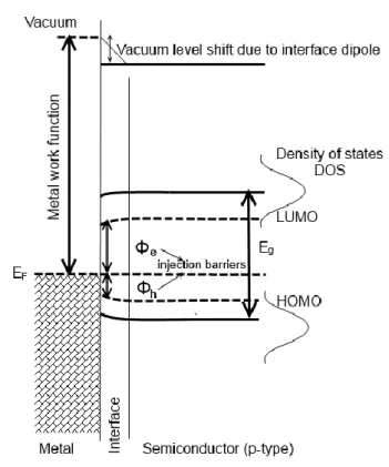
Metal electrode/Organic semiconductor interfaces: The metal electrode/organic semiconductor interface is of high importance for thin film transistors operation. Metal electrode surfaces are prone to form dipoles even when they are stored in relatively dry inert gas atmosphere, leading to possible changes in the work function of the metal electrodes (Figure 2-11) [131]. Interface energetics are usually studied by spectroscopic techniques i.e. photoemission spectroscopy [132]. Because metal electrodes are used for extracting (injecting) charge carriers from the organic semiconductor, a good matching between the HOMO (LUMO) level of the semiconductor with the electrode work function is desired [77], [131], [132], [133], [134], [135], [136], [137], [138].
Ambipolar charge carrier transport, i.e. simultaneous electron and hole transport, is also possible under certain conditions e.g. with small energy band gap semiconductors (Eg< 2 eV) [5],
[139], [140], [141]. N-type charge transport is rarely observed for organic semiconductors because of the unfavorable location of their LUMO level with respect to commonly employed metal electrode materials such as Au. In electrochemical terms, organic semiconductors usually have low electrochemical reduction potentials [142].
In this thesis, Article 3 reports ambipolar organic thin film transistors based on a soluble pentacene derivative. HOMO and LUMO levels of this novel pentacene derivative were compared with that of pentacene. The relative placement of the LUMO level of the new molecule was found to be closer to the Au work function leading to electron injection from the molecule to the metal electrode. In Article 4, p-type and ambipolar π-conjugated molecules making use of azomethines (–N = C–) compared to more conventional (–C = C–) coupling protocols are demonstrated. The position of the HOMO and LUMO levels with respect to Au electrode work function as well as the effect of electron donating groups in the molecular structure were discussed to explain the p-type and ambipolar behavior of the molecules [95]. We also studied the effect on the location of the HOMO and LUMO energy [4] of the oxidation level at the central sulfur in novel dithienothiophene oligomers. Although we did not observe an n-type behavior or ambipolarity for thin films prepared from these molecules, we observed p-type conductivity in the channel and the highest mobility was observed for oligomers with the lowest
hole injection barrier, i.e. with the smallest difference in energy between the location of the HOMO levels and the Fermi energy of the metal electrode.
WO3/ITO interfaces: ITO is a commonly used transparent conductive oxide in display devices
and photovoltaic cells with a Fermi level located at 4.7 eV with respect to vacuum [143]. The conduction band and valence band edges of WO3 depend on the structure of the material and the
experimental environment and they are approximately located at 4.6 and 7.3 eV (Figure 2-12) [144], [145], [146], [147], [148], [149].
Figure 2-11 Scheme of the metal/p-type semiconductor interface. The hole (electron) injection barrier, Фh (Фe), is the difference between HOMO (LUMO) level of the organic semiconductor
and the Fermi level of the metal. Фh is small enough for hole injection. The effect of an applied
bias at the gate electrode on the HOMO and LUMO levels at the interface is also shown by a small bending. GDOS is also shown. (Adapted from [71])
Figure 2-12 ITO/WO3 interface energy band diagram. The Фe for electron injection is <0.1eV.
2.3.3 Gate dielectric
Semiconductor/gate dielectric interface is as important as the semiconductor/metal interface. The relative dielectric constant ε is related to the capacitance, C, of the material (Eqn 2-1):
Eqn 2.1
In this equation, ɛ˳ is the permittivity of free space (8.85 10-12 F/m), A is the surface area of the gate dielectric and t is its thickness. Gate dielectric selection criteria depend on dielectric constant and thickness, which needs to be as low as possible. Nevertheless, thin gate dielectrics can show high leakage current at the semiconductor gate electrode interface. Therefore the best dielectrics are those with high dielectric constants which can be deposited as very thin layers [150], [151].
Organic semiconductor/Gate dielectric interfaces: In organic thin film transistors the gate dielectric importance is two-fold: (i) functional properties of the films highly depend on the molecular ordering at this interface and (ii) the interfacial chemistry affects charge carrier trap density [152]. The arrangement of the molecules at the interface results in different
morphologies, structure and textures, i.e. π-π stacking vertical or parallel to the source and drain electrodes [5], [153], [154], [155], [156], [157], [158]. Considering that the field effect transistor operation depends on the first few nanometers at the vicinity of the organic semiconductor/gate dielectric interface, the importance of such interface can be easily understood [159]. Studies on benchmark pentacene and tetracene films showed that the gate dielectric surface roughness is an important parameter that affects the morphology, which in turn affects the transistors performance [130], [152], [160], [161]. A high roughness of the gate dielectric leads to smaller islands. The connectivity of the islands and the surface coverage play an important role in the performance of thin film transistors [152].
Second, the interfacial chemistry plays an important role in the charge carrier trap density at the semiconductor/gate dielectric interface. To improve the quality of this interface, passivating self assembled monolayers can be used [162], [163], [164]. In this Ph.D. work, SiO2
gate dielectric was treated by hexamethyldisilazane (HMDS) [5], [95], [163], [165], [166]. A clear difference in device operation between HMDS treated and non-treated samples was observed, with low surface coverage observed for non-treated substrates [152], [167], [168]. WO3/Ionic liquid interfaces: Electrolyte gating is an effective approach to lower the operating
voltage of transistors. The structure of the electrical double layer forming at the semiconductor/electrolyte interface is one of the keys to the effectiveness of the gating [169], [170], [171], [172], [173][173]. The structure of the electrical double layer depends on a number of factors, such as the anion and cations constituting the electrolyte, the ionicity of the ionic liquid (i.e. the degree of dissociation of the ions) the applied electrical bias, the purity of the ionic liquid, the nature of the working electrode and the working electrode surface [174]. Because of the high capacitance values that can be achieved (eqn 2.1) using electrical double layers the amount of charge carriers accumulated in the semiconductor films is also remarkably high, for relatively low operating voltages [175], [176], [177][178].
2.3.4 Organic thin film transistor operation
Organic thin film transistors work most frequently in accumulation mode [30]. The operation of organic thin film transistors is generally described making use of the metal oxide insulator field effect transistor model.
The operation can be divided into three regions: cut-off, linear region and saturation region (Figure 2-13). This model assumes a long transistor channel length where the electrical field created by the gate electrode bias overcomes the transverse electrical field in the channel, i.e. the gradual channel approximation [179], [180].
Threshold voltage (VTh) is defined as the minimum gate voltage that is required to
electrostatically induce the channel [30], [181]. The current in the channel starts to flow in the transistor channel when the threshold potential is exceeded (VGS>VTh).
Figure 2-13 Schematic illustration of organic thin film transistor operation. Circles in the semiconductor layer illustrate the holes during different stages of transistor operation. In (a) Cut-off, (b) Linear region and (c) the saturation region are illustrated.
In cut-off conditions, where VGS<VTh no or very low current flows in the transistor
channel, which is called the off-current (Figure 2-13a).
In the linear region, at VDS< VGS-VTh and VGS>VTh the Fermi energy level raises and the
semiconductor energy bands bend upwards (Figure 2-13b). A thin sheet of mobile charge carriers is induced into the channel. At this point the transistor channel behaves like a resistor and the
current depends on the accumulation of positive charges as a function of the gate voltage. The resistance of the channel remains almost constant in this region, where the drain current IDS is
proportional to the VDS. The current collected when the channel is open is called the on-current.
At higher VDS values, the amount of induced mobile charge carriers decreases and the slope of the
IDS vs VDS curve starts to decrease because of increasing resistance. At VDS = VGS -VTh pinch-off
occurs and the charge concentration at the drain electrode is said to become zero. In the saturation region, when VDS>VGS-VTh and VGS>VTh thecurrent in the channel saturates.
Figures of merit for transistor operation is further discussed in section 2.3.6 combined with electrolyte gated transistor characterization.
2.3.5 Mechanism of electrolyte gating
Low operating voltages can be achieved with thin gate dielectric layers and high dielectric constants [160], [182], [183] but also with more unconventional approaches such as electrolyte gating, which can take place by two different mechanisms: electrostatic (electric double layer) and electrochemical (Figure 2-14). In the electrostatic mechanism, the electrical double layer forming at the semiconductor/electrolyte interface upon the application of a gate voltage results in the electrostatic doping of the semiconductor [25], [26], [32], [72], [178], [184]. Electrical double layer capacitances per unit area are approximately 10 - 500 µF cm-2 whereas the typical capacitance of a 200 nm-thick SiO2 dielectric layer is of tens of nF cm-2. In the electrochemical
mechanism of electrolyte gating ion intercalation takes place [185], [186], [187]. In principle, the sizes of the ions constituting the ionic liquids are such that the electrochemical mechanism is unfavorable compared to the electrostatic.
2.3.6 Transistor figures of merit
Thin film transistor characteristics are mainly evaluated by acquisition of the output (IDS
vs VDS) and transfer transistor characteristics (IDS vs VGS) [188], [189]. The parameters used in
describing the transistor operation are listed in Table 2-2. Charge carrier mobility (µe and/orµh),
threshold voltage (VTh) and ION/IOFF ratio of the transistor are the three basic parameters that
Figure 2-14 General structure of an electrolyte gated transistor (left). Electrochemical mechanism (top right) and electrostatic mechanism (bottom-right) of doping during electrolyte gating.
Charge carrier mobilities of devices in the linear (µLin) and in the saturation (µSat) region can be
calculated by use of the equations 2.2 and 2.3:
Eqn 2.2
The mobility at saturation can be determined by substituting VDS=VGS-VTh in Eqn 2.2 and
simplifying to:
VTh is deduced from the maximum slope of the transfer curve (sqrt IDS vsVGS). ION/IOFF
ratio gives a hint on the ability of the device to switch on and off and is calculated by dividing the max IDS value by the minimum IDS value of the transfer curve (LogIDS vs VGS).
Table 2-2 Transistor parameters
Parameter Symbol Unit
W Channel width µm
L Channel length µm
Ci
CEDL
Specific gate capacitance
Electrical double layer capacitance
ID Drain current A IG Gate current A IS Source current A VGS Gate-source voltage V VTh Threshold voltage V VDS Drain-source voltage V µe µh Electron mobility Hole mobility
CHAPTER 3
EXPERIMENTAL METHODS AND TECHNIQUES
3.1 Sample preparation
In this section of Chapter 3, a brief introduction to organic thin film transistor and electrolyte gated thin film transistor structures is given. Afterwards, the procedures for substrate cleaning and substrate surface modification processes are illustrated. Solution preparation and deposition by solution based techniques together with post-deposition steps are detailed. For electrolyte gated thin film transistors, an additional step for PDMS well preparation and ionic liquid confinement step is presented.
3.1.1 Organic thin film transistors: device structure
Organic semiconductors were tested on bottom contact/bottom gate transistor substrates making use of circular Au source and drain interdigitated electrodes photo-lithographically patterned on SiO2 (195 nm-thick, Ci = 1.77·10-8 F/cm2), thermally grown on heavily doped Si(n+)
wafers (resistivity 0.001-0.005 Ohm cm-1) (Figure 3-1). Au has a Fermi level of 4.4 eV [100]. An advantage of using Au electrodes is that they do not get oxidized in ambient conditions as Ca, Mg, Al electrodes. Characteristics of the transistor structures used for organic thin film transistor studies are listed in Table 3-1 and Table 3-2 for the channel and the material, respectively.
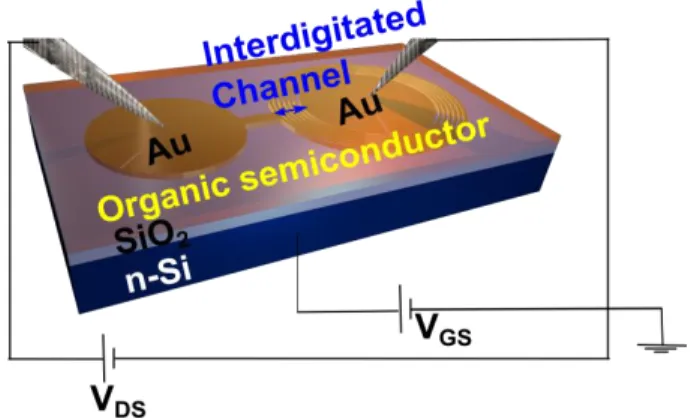
Figure 3-1 Bottom contact-bottom gate (Si (n+)) transistor substrate with interdigitated pre-patterned Au electrodes (30 nm thick) and SiO2 (195 nm) gate dielectric coated with an organic
Table 3-1 Transistor channel widths (W) and lengths (L) in organic thin film transistors investigated in this work.
W (µm) L (µm)
Interdigitated devices 6 41000
20 41800
40 18800
Table 3-2 Gate dielectric properties for organic thin film transistors investigated in this work. SiO2 Relative Dielectric Constant 3,9
SiO2 Thickness [nm] 195
SiO2 Absolute Dielectric Constant [F/m] 8,854187818×10⁻¹²
Ci [F/m2] 1,770837564×10⁻⁴
3.1.2 Electrolyte gated thin film transistors: device structure
The effect of the electrolyte gating on the WO3 thin films was tested in the electrolyte
gated transistor configuration (Figure 3-2). In this configuration, the channel conductivity is controlled by a gate electrode that is immersed into the electrolyte that is confined by a PDMS well positioned in correspondence of the semiconductor channel.
3.1.3 Ionic liquids
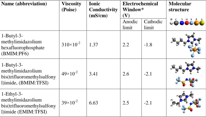
Ionic liquids were used as electrolytes for electrolyte gated thin film transistors. During the work conducted in the frame of this thesis ionic liquids were selected as the gating medium (Table 3-3) due to their non-volatile and highly conductive nature. Ionic liquids also posses high chemical stability with relatively wide electrochemical windows [190]. The electrochemical window is defined as the voltage range in which the electrolyte is electrochemically stable. Ionic liquids are molten salts that do not contain any solvent; they are solely formed of anion and cation pairs.
Figure 3-2 Electrolyte gated transistor built on a glass substrate with patterned ITO electrodes. The channel is in contact with the electrolyte, confined in a PDMS well on top of the channel. An electrode immersed into the electrolyte is used to gate the channel.
Table 3-3 Properties of the ionic liquids used for the characterization of electrolyte gated transistors.
Name (abbreviation) Viscosity (Poise) Ionic Conductivity (mS/cm) Electrochemical Window* (V) Molecular structure Anodic limit Cathodic limit 1-Butyl-3-methylimidazolium hexafluorophosphate (BMIM:PF6) 310×10-2 1.37 2.2 -1.8 1-Butyl-3-methylimidazolium bis(trifluoromethylsulfony l)imide, (BMIM:TFSI) 49×10-2 3.41 2.6 -2.1 1-Ethyl-3-methylimidazolium bis(trifluoromethylsulfony l)imide (EMIM:TFSI) 39×10-2 6.63 2.5 -2.1
![Figure 2-4 Energy band diagrams for an ordered molecular crystal and a disordered molecular material [71], [87], [88]](https://thumb-eu.123doks.com/thumbv2/123doknet/2333440.32207/29.918.284.640.426.718/figure-energy-diagrams-ordered-molecular-disordered-molecular-material.webp)