UNIVERSITÉ DE MONTRÉAL
INNOVATIVE MILLIMETER-WAVE COMPONENTS BASED ON MIXED
SUBSTRATE INTEGRATED DIELECTRIC-METALLIC WAVEGUIDES
JAWAD ARIF AL ATTARI
DÉPARTEMENT DE GÉNIE ÉLECTRIQUE ÉCOLE POLYTECHNIQUE DE MONTRÉAL
THÈSE PRÉSENTÉE EN VUE DE L’OBTENTION DU DIPLÔME DE PHILOSOPHIAE DOCTOR
(GÉNIE ÉLECTRIQUE ) JUIN 2013
UNIVERSITÉ DE MONTRÉAL
ÉCOLE POLYTECHNIQUE DE MONTRÉAL
Cette thèse intitulée:
INNOVATIVE MILLIMETER-WAVE COMPONENTS BASED ON MIXED
SUBSTRATE INTEGRATED DIELECTRIC-METALLIC WAVEGUIDES
présentée par : AL ATTARI Jawad Arif
en vue de l’obtention du diplôme de : Philosophiæ Doctor a été dûment acceptée par le jury d’examen constitué de : M. KASHYAP Raman, Ph.D., président
M. WU Ke, Ph.D., membre et directeur de recherche M. TATU Serioja, Ph.D., membre
DEDICATION
ACKNOWLEDGEMENTS
The author is indebted to many people without whom this report would not have seen light. First of all, I would like to express my gratitude to my PhD advisors, Prof. Ke Wu, who offered unconditional support and motivation. His creativity, perseverance and reassurance thrust me to attain the furthest of frontiers possible in academic research.
I would also like to thank all the personnel at the Poly-Grames Research Center, in particular Mr. Jules Gauthier, Mr. Traian Anretsu, Mr. Steve Dubé and Mr. Maxim Thibault, whose technical assistance was essential for the realization of the prototypes. Special thanks are extended to Mrs. Ginette Desparois and Mrs. Nathalie Lévesque for guiding me through the administrative procedure and to Mr. Jean-Sébastien Décarie for assistance with IT-related issues.
I am also grateful to Dr. Tarek Djerafi and other colleagues, especially Dr. David Dousset and Dr. Simon Hermour, for all the intellectual and technical advice and insight.
A special thank goes to the members of the examination jury, for the time they invested in reading this thesis and the invaluable comment they provided.
Last but not least, I am truly indebted to my parents who invested all their passion, time and resources to raise me to this level of academia. I also thank my relatives for their sincere moral support.
RÉSUMÉ
En recherche, un défi majeur pour l'onde millimétrique et les bandes Terahertz (THz) sont l'intégration des différents composants d'une manière compacte, efficace et à faible coût. La notion de circuits intégrés aux substrats (CIS) muni d'une variante de tradition pour une essentiel conception en simplifiant l'intégration du guide d'ondes rectangulaire (donc le GIS) avec d'autres lignes de transmission planaires telles que les lignes microbande et CPW. Bien que cette amélioré considérable conçue aux bandes de fréquences K et X, des limitations persistent dans des bandes plus élevées, en particulier la bande W. Nouvelles implémentations du concept de CIS en utilisant des guides d'ondes diélectriques, tels que le guide d’onde diélectrique non rayonnant (guide NRD), ont ainsi été proposées et avec un certain nombre de circuits à base de guide d’onde diélectrique non rayonnant intégrés aux substrats (SINRD) ont été conçus à des fréquences W-bande. Néanmoins, les critères de conception des guides rigides SINRD sont limités par leurs utilisations pratiques.
Dans cette thèse, une version modifiée du guide SINRD, basée sur le guide image NRD (iNRD), est proposé. Ce travail sera le premier à étudier la faisabilité de la conception du guide iNRD avec le concept du CIS. La polyvalence du guide image SINRD résultant (iSINRD) sera démontrée par la conception d'un certain nombre de composants passifs qui fonctionnent à la fréquence centrale 94 GHz à la bande W.
Plus précisément, les contributions suivantes ont été étudiées aux deux fréquences 88 GHz et 94 GHz:
1. Une méthodologie de conception pour l’optimisation des circuits du classe NRD. À date, Cette méthode est l’alternative le plus simple et la méthode la plus informative.
2. Un certain nombre de lignes de transmission pour guidage iSINRD qui sont conçus avec des différents profils de perforation et avec un nombre différent de lacunes sur la paroi métallique de l’image vertical.
3. Des Guides iSINRD à angles aigus à large bande et à bande étroite.
4. Deux configurations différentes de coupleurs directionnels pour le guide iSINRD qui prennent en charge le mode double (LSM10 et TE20 modes) et le fonctionnement bi-bande
(Couplage de 0-dB tandis que l'autre avec 3-dB de couplage). La bande de la matière à l'accouplement 0-dB est exclusive pour une des configurations. Ainsi, un total de six coupleurs directionnels est présenté.
5. Une structure croisée qui utilise la nature bi-bande selon l'une des configurations pour coupleur directionnel iSINRD est conçu. Dans cette structure, la LSM10 et les modes TE20
qui sont simultanément alimentés aux deux ports d'entrée sont collectées au niveau des ports opposés par l'intermédiaire du mécanisme de couplage 0-dB.
6. Hybride d'iSINRD 180° fonctionnant en mode LSM10.
7. Coupler Asymmetric d’iSINRD et SIW en modes LSM10 et TE01
8. Orthogonal Mode Transducer compact et simple (OMT ou duplexeur de polarisation), avec les modes orthogonaux ayant les modes LSM10 et TE20.
9. Technique du mode correspondant est utilisé pour construire un coupleur en croix très compact iSINRD.
10. Un iSINRD Té magique circuit est développé en modifiant les longueurs de l'un des bras du coupleur croix iSINRD.
ABSTRACT
A major challenge facing the millimetre-wave and terahertz (THz) research fields, is the integration of different components in a compact, efficient and low-cost fashion. The concept of substrate integrated circuits (SICs) provides a vital alternative to traditional design by simplifying the integration of the rectangular waveguide (thus the SIW) with other planar transmission lines such as microstrip and CPW lines. While this has substantially enhanced the design techniques at the X- and K-band frequencies, limitations still persist at higher bands, especially the W-band and beyond. New implementations of the SICs concept using dielectric waveguides such as the substrate integrated non-radiative dielectric (SINRD) guide, were thus proposed and a number of SINRD-based circuits were designed at the W-band frequencies. Nonetheless, the SINRD guide has rigid design criteria that limit its practical use.
In this thesis, a modified version of the SINRD guide, based on the image NRD (iNRD) guide, is investigated. This work will be the first to investigate the feasibility of designing the iNRD guide with the SICs concept. The versatility of the resulting image SINRD (iSINRD) guide will be demonstrated by designing a number of passive components that operate at the W-band centre frequency of 94 GHz.
Specifically, the following contributions have been made at the W band frequencies of 88 GHz and 94 GHz:
1. An optimised design methodology of the NRD-class circuits. This method is a simpler alternative to earlier methods and is more informative.
2. A number of iSINRD guide transmission lines that are designed with different perforation profiles and with a different number of gaps in the metal wall.
3. Broadband and narrowband iSINRD guide sharp corners
4. Two different configurations of iSINRD guide directional couplers that support dual mode (LSM10 and TE20 modes) and dual band operation (one band for 0-dB coupling while the
other for 3-dB coupling). The band pertinent to the 0-dB coupling is exclusive for one of the configurations. Thus, a total of six directional couplers are presented.
5. A cross-over structure that utilizes the dual band nature of one of the iSINRD directional coupler configurations is designed. In this structure, the LSM10 and TE20 modes that are
concurrently fed at the two input ports are collected at the opposite ports through the mechanism of 0-dB coupling.
6. A 180o iSINRD hybrid based on the LSM10 mode
7. An asymmetric iSINRD-SIW coupler based on the LSM10 and TE01 modes
8. A compact and simple orthogonal mode transducer (OMT), with the orthogonal modes being the LSM10 and the TE20 modes
9. Even-odd mode analysis technique is used to construct a very compact iSINRD cruciform coupler.
10. An iSINRD magic-T circuits is developed by modifying the lengths of one of the arms of the iSINRD cruciform coupler.
TABLE OF CONTENTS
DEDICATION ... III ACKNOWLEDGEMENTS ... IV RÉSUMÉ V ABSTRACT ...VII TABLE OF CONTENTS ... IX LIST OF TABLES ...XII LIST OF FIGURES ... XIII LIST OF SYMBOLS AND ABBREVIATIONS... XXI LIST OF ANNEXES ... XXIVINTRODUCTION ... 1
Chapter 1 INVESTIGATION OF THE IMAGE SINRD GUIDE AT THE W-BAND FREQUENCIES ... 5
1.1 Introduction ... 5
1.2 Review of the NRD and SINRD Waveguides ... 5
1.2.1 Geometry of the NRD and SINRD Guides ... 5
1.2.2 Dominant Modes ... 7
1.3 Design Challenges of the SINRD Guide ... 11
1.4 Proposed Alternative Design Approach of the SINRD Guide ... 12
1.4.1 The Image SINRD (iSINRD) Guide ... 12
1.4.2 Eigen-Mode Analysis of Periodic SINRD Guides ... 14
1.4.3 The SINRD Guide as a Generalised NRD Guide ... 15
1.4.4 The Minimum Operating Frequency, fn and the Choice of Thickness a ... 17
1.4.6 Determining channel width, b and effective permittivity ε2 ... 20
1.4.7 Relating ε2 to Perforation Dimensions... 23
1.4.8 Note on Determining ε2 ... 26
1.5 Loss Analysis ... 26
1.6 Discussion ... 28
Chapter 2 IMPLEMENTATIONS OF THE iSINRD GUIDE AT THE W-BAND FREQUENCIES ... 30
2.1 Introduction ... 30
2.2 Continuous and Discontinuous Walls ... 30
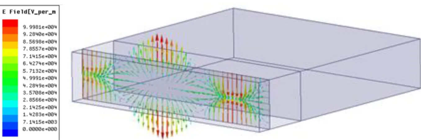
2.3 iSINRD Guide Bends ... 32
2.4 Experimental Results and Discussion ... 38
2.4.1 iSINRD Transmission Lines ... 38
2.4.2 iSINRD Guide with Gaps in the Metal Image Wall... 42
2.4.3 iSINRD Guide Bends ... 44
Chapter 3 THE iSINRD GUIDE IN THE CONTEXT OF DIRECTIONAL FORWARD COUPLERS ... 46
3.1 Introduction ... 46
3.2 Symmetric Directional Couplers based on the iSINRD Guide ... 47
3.2.1 Type A Coupler ... 47
3.2.2 Type B Coupler ... 51
3.2.3 Dual-mode iSINRD Cross-Over Structure ... 56
3.3 The iSINRD-iSIW Asymmetric Directional Coupler ... 57
3.3.1 Principle of Operation ... 58
3.3.2 Parametric Study ... 59
3.5 Experimental Results and Discussion ... 63
Chapter 4 THE iSINRD GUIDE IN THE CONTEXT OF CRUCIFORM CIRCUITS ... 70
4.1 Introduction ... 70
4.2 The iSINRD Cruciform Coupler ... 71
4.2.1 Coupling Mechanism ... 71
4.2.2 Even-Odd Mode Analysis ... 71
4.3 An Asymmetric Planar iSINRD Cruciform Magic-T ... 78
4.3.1 Principle of Operation ... 80
4.4 A W-Band Ortho-mode Transducer Based on the Image SINRD (iSINRD) Guide ... 83
4.4.1 Mechanism of the Proposed OMT ... 85
4.4.2 Dimensions of the proposed OMT ... 86
4.5 Experimental Results and Discussion ... 93
4.5.1 The iSINRD Cruciform Coupler ... 93
4.5.2 The iSINRD Cruciform Magic-T ... 95
4.5.3 The iSINRD-SIW Ortho-Mode Transducer ... 97
CONCLUSION AND OUTLOOK ... 99
BIBLIOGRAPHY ... 103
LIST OF TABLES
Table 1.1: Comparison of different dielectric materials at different millimeter-wave
frequencies………..16
Table 1.2: Comparison of dielectric losses in different waveguides at 94 GHz………28
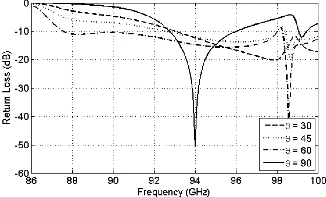
Table 2.1: Correlation between the bend angle theta and the return loss at 94 GHz…………...37
Table 3.1: Key dimensions of the iSINRD directional forward couplers………..51 Table 4.1: Comparison between the proposed iSINRD/SIWOMT and other W-Band OMT’s….93
LIST OF FIGURES
Figure 1 : Upper segment: exploded views of the rectangular waveguide (left), the NRD guide (centre) and the image guide (right). Lower segment: exploded views of the SIW (left), the SINRD guide (centre) and the SIIG (right). Orange: metal covers, black: metal vias, grey: insulating substrate of the SIIG, white: air vias, dark green: dielectric substrate which contains the waveguide. ... 3 Figure 2 : Cross-sectional front view of the E-field lines of the LSM10 mode in the SINRD guide
(left) and the image SINRD (iSINRD) guide (right). ... 3 Figure 1-1: The NRD guide (top, left) and the SINRD guide (top, right). Bottom: Cross-sectional front view of the SINRD guide. ... 6 Figure 1-2: Perforation Profiles (top view): circular profile (left), and square (right) perforation profiles; to name a few. ... 7 Figure 1-3: Cross-sectional front view of the E-field lines of the LSM10 (top), TE10 (bottom. right)
and LSE10 (bottom, left) modes in the (SI)NRD guide. Encircled × (into page) or · (out of
page) represent the longitudinal Ez component. ... 7
Figure 1-4: The cross-sectional front view of the E-field lines of the LSM10 (left) and TE20 (right)
modes in the iSINRD guide. ... 12 Figure 1-5: A 3-D view of a unit-cell of the iSINRD waveguide in HFSS Eigen-mode solver together with a cross-sectional front view of the simulated E-field of the LSM10 mode. ... 15
Figure 1-6: The cross-sectional front view of a generalised NRD guide. ... 16 Figure 1-7: Frequency fx-fn bands corresponding to different thicknesses computed with [62]. ... 18
Figure 1-8: Comparison of two operation bands: a/λg = 0.381 and a/λg = 0.635. Operation at 94
GHz with a/λg = 0.381 using Alumina is impossible. ... 19
Figure 1-9: Choosing the optimum fx-fn band for W-band operation. ... 19
Figure 1-10: Different dielectrics with unequal thicknesses corresponding to the same fg-band. . 20
Figure 1-11: Operation curves, within an fg-band, for different values of the width, b, and for a
Figure 1-12: Choosing the width, b, based on the desired εr2/εr1 ratio operating frequency, fg. .... 22
Figure 1-13: The variation of the LSM10 bandwidth with the width, b, for different ε2/ε1 ratios. .. 22
Figure 1-14: Relating εr2/εr1 to p/λg (p = gap + D) for the circular via profile. ... 24
Figure 1-15: Relating εr2/εr1 to p/λg (p = gap + w) for the square-via profile. ... 25
Figure 1-16: Propagation curves of the TE20 and LSM10 modes in the iSINRD guide. ... 25
Figure 1-17: Attenuation factor due to conductor, dielectric and total losses of the iSINRD and SINRD guides. ... 27 Figure 1-18: Total attenuation in the iSINRD and SINRD guides compared to the SIW. ... 28 Figure 2-1: The leakage loss in discontinuous-iSINRD guide compared to continuous-iSINRD guide (0 gaps). ... 31 Figure 2-2: Current distribution of the E-field of the LSM10 mode in the continuous-wall iSINRD
guide. ... 31 Figure 2-3: Current distribution of the E-field of the LSM10 mode in the discrete-wall iSINRD
guide. ... 32 Figure 2-4: Top view of two possible geometries of the iSINRD guide bends (left and center). Right: the arms that result as a consequence of decomposing the bends I or II along the symmetry line m-n and thereafter applying PEC and PMC boundary conditions. ... 33 Figure 2-5: The simulated (S) and calculated (C) S-Parameters of the Case I iSINRD guide bend.
... 34 Figure 2-6: The simulated (S) and calculated (C) S-Parameters of the Case II iSINRD guide bend.
... 34 Figure 2-7: A 3-D plot of the electric field of the LSM10 mode in the Case I iSINRD guide bend.
... 35 Figure 2-8: A 3-D plot of the electric field of the LSM10 mode in the Case II iSINRD guide bend.
... 35 Figure 2-9: Varying the bend angle α. ... 36 Figure 2-10: Variation of the return loss with respect to the bend angle (Case I). ... 36
Figure 2-11: Variation of the return loss with respect to the bend angle (Case II). ... 37
Figure 2-12: Intended dimensions (solid) and fabricated dimensions (dashed). ... 38
Figure 2-13: Top view of a fabricated iSINRD guide (continuous metal wall, circular profile). .. 39
Figure 2-14: Top view of a fabricated iSINRD guide (continuous metal wall, square profile). .... 39
Figure 2-15: Top view of the fabricated iSINRD guide prototype (continuous metal wall, Rogers RO6010 substrate). ... 39
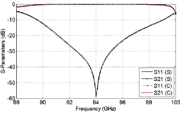
Figure 2-16: The simulated S-parameters of the circular via and square via profiles. ... 40
Figure 2-17: The simulated and measured S-parameters for the circular via iSINRD guide. ... 40
Figure 2-18: Simulated (S) and measured (M) S-parameters for the square via iSINRD guide. ... 41
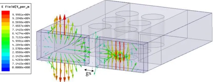
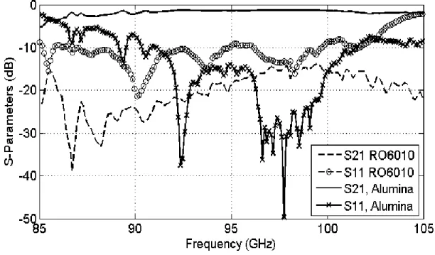
Figure 2-19: Measured S-parameters for the circular via Alumina and RO6010 iSINRD guides. 41 Figure 2-20: Top view of an iSINRD guide with one gap (left) and three gaps (right). ... 42
Figure 2-21: The simulated (S) and measured (M) return losses for different gaps. ... 43
Figure 2-22: The simulated (S) and (M) measured insertion losses for different gaps. ... 43
Figure 2-23: Top view of a fabricated Case I iSINRD guide bend. ... 44
Figure 2-24: Top view of a fabricated Case II iSINRD guide bend. ... 44
Figure 2-25: The simulated (S) and measured (M) results of the Case I iSINRD bend. ... 45
Figure 2-26: The simulated (S) and measured (M) results of the case II iSINRD bend. ... 45
Figure 3-1: Continuous coupling between two parallel waveguides/lines. ... 47
Figure 3-2: Discrete coupling between two parallel waveguides/lines. ... 47
Figure 3-3: A schematic top-view of the Type A iSINRD directional coupler. ... 48
Figure 3-4: Coupling level, in dB, as a function of the number of coupling vias. ... 49
Figure 3-5: Simulated S-Parameters of the Type A iSINRD directional. ... 49
Figure 3-6: The phase imbalance with respect to frequency of the Type A iSINRD directional coupler. ... 50
Figure 3-7: A top view plot of the E-field of the LSM10 mode in a Type A iSINRD directional
coupler. ... 50
Figure 3-8: A schematic top-view of the Type B iSINRD directional coupler. ... 52
Figure 3-9: The E-fields of the LSM10 (left) and the TE11 (right) modes. ... 52
Figure 3-10: Coupling level, in dB, as a function of the number of coupling vias at 94 GHz. ... 53
Figure 3-11: The simulated S-Parameters of the Type B iSINRD directional (LSM10 operation). 53 Figure 3-12: The phase variation with respect to frequency of the LSM10 Type B iSINRD directional coupler. ... 54
Figure 3-13: A top view plot of the E-field of the LSM10 mode in a Type B iSINRD directional coupler. ... 54
Figure 3-14: Coupling level, in dB, as a function of the number of coupling vias at 94 GHz (TE20 operation). ... 55
Figure 3-15: The simulated S-Parameters of the Type B iSINRD directional (TE20 operation). .. 55
Figure 3-16: Phase variation with respect to frequency of the TE20 Type B iSINRD directional coupler. ... 56
Figure 3-17: Coupling level, in dB, as a function of the number of coupling vias at 88 GHz. ... 56
Figure 3-18: A schematic top-view of the iSINRD-iSIW directional coupler. ... 57
Figure 3-19: A cross-sectional front-view of the electric field lines of the TE10 (left) and TE01 (right) modes in the SIW. ... 59
Figure 3-20: Coupling level, in dB, as a function of the number of coupling vias for the asymmetrical iSINRD-iSIW directional coupler. ... 59
Figure 3-21: The simulated S-Parameters of the iSINRD-iSIW directional coupler. ... 60
Figure 3-22: Phase variation with respect to frequency of the asymmetrical iSINRD-iSIW directional coupler. ... 60
Figure 3-23: A 3-D filed plot of the LSM10 mode in an asymmetrical iSINRD-iSIW directional coupler. ... 61
Figure 3-24: Top view of a Type B 180o hybrid based on the iSINRD guide Type B directional
coupler. ... 62
Figure 3-25: Phase variation with respect to frequency of an iSINRD guide 3-dB 180o hybrid. .. 62
Figure 3-26: Top view of a fabricated Type A iSINRD directional coupler. ... 64
Figure 3-27: Top view of a fabricated Type B iSINRD coupler (LSM10 operation). ... 64
Figure 3-28: Top view of a fabricated Type B iSINRD coupler (TE20 operation). ... 65
Figure 3-29: Top view of a fabricated iSINRD-iSIW asymmetrical directional coupler. ... 65
Figure 3-30: Top view of a fabricated iSINRD 180o hybrid. ... 66
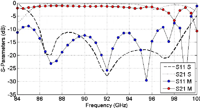
Figure 3-31: Simulated (S) and measured (M) S-parameters of the iSINRD Type A coupler (LSM10 operation). ... 66
Figure 3-32: Simulated (S) and measured (M) S-parameters of the LSM10 mode Type B iSINRD coupler, including the 88 GHz cross-over coupler. ... 67
Figure 3-33: Simulated (S) and measured (M) S-parameters of the TE20 mode Type B iSINRD coupler, including the 88 GHz cross-over coupling. ... 67
Figure 3-34: Simulated (S) and measured (M) S-parameters of the asymmetric iSINRD-iSIW coupler, including the cross-over coupler (TE20 operation). ... 68
Figure 3-35: Simulated (S) and measured (M) phase imbalance of the four different iSINRD 3-dB directional couplers. ... 68
Figure 3-36: Simulated (S) and measured (M) phase imbalance of the in-phase operation of the iSINRD 3-dB 1800 hybrid. ... 69
Figure 3-37: Simulated (S) and measured (M) phase imbalance of the out-of-phase operation of the iSINRD 3-dB 1800 hybrid. ... 69
Figure 4-1: (a) Top view of the proposed iSINRD coupler (left), 3-D view of the proposed coupler (top, right) and the E-field of the LSM10 mode (front view, bottom right). Green: Substrate; white: air vias, black: PEC image plane; orange: metal covers. (b) Top view description of the proposed iSINRD coupler and its bend and arm decomposition. Solid: PEC; dashed: PMC. ... 72
Figure 4-2: Phase difference between arms A and C, and arms B and D as a function of the
iSINRD guide width, b, at 94 GHz. ... 74
Figure 4-3: Phase diagram of arms A and B as a function of iSINRD guide width, b, at 94 GHz. ... 75
Figure 4-4: The simulated (S) and calculated (C) S-parameters of the iSINRD cruciform coupler obtained from the configurations in Figure 4-5 below. ... 75
Figure 4-5: The incorrect setup of the arms in [51]. ... 76
Figure 4-6: The simulated (S) and calculated (C) S-parameters of the iSINRD cruciform coupler obtained from the configurations in ... 76
Figure 4-7: The correct setup of the arms in [51]. ... 77
Figure 4-8: Phase variation of the iSINRD cruciform coupler with respect to frequency. ... 77
Figure 4-9: A 3-D plot of the electric field of the LSM10 mode in the iSINRD cruciform coupler. ... 78
Figure 4-10: A 3-D view of a conventional rectangular waveguide magic-T power divider. ... 79
Figure 4-11: Out-of-phase power division of the E-plane T-junction; black arrows represent electric field lines. Grey arrows represent direction of power flow. ... 79
Figure 4-12: A 3-D view (left) and a top view of the asymmetric iSINRD cruciform magic-T. . 81
Figure 4-13: Phase difference relative to the ports 1 (in-phase) and 4 (out-of-phase). ... 81
Figure 4-14: Top view plot of the E-field of the LSM10 mode due to feeding at input 3 (left) and input 2 (right). ... 82
Figure 4-15: Top view plot of the E-field of the LSM10 mode due to in-phase (left) and out-of-phase (right) simultaneous excitation of ports 2 and 3, respectively. ... 82
Figure 4-16: A 3-D view of a typical narrow-band, acute-angle OMT. ... 83
Figure 4-17: Top view of the proposed iSINRD-SIW OMT. ... 84
Figure 4-19: Insertion loss (S31) for different values of d (the LSM10 mode) as function of
frequency. ... 86
Figure 4-20: Insertion loss (S21) for different values of d (the TE20 mode), as a function of frequency. ... 87
Figure 4-21: The effect of inset distance t on the S-parameters of the TE20 mode. Black: transmission; red: reflection; blue: isolation. ... 87
Figure 4-22: The effect of inset distance t on the S-parameters of the LSM10 mode. Black: transmission; red: reflection; blue: isolation. ... 88
Figure 4-23: A 3-D plot of the E-field of the LSM10 mode in the iSINRD-SIW OMT. ... 88
Figure 4-24: A 3-D plot of the E-field of the TE20 mode in the iSINRD-SIW OMT. ... 89
Figure 4-25: The top view of a back to back, four-port iSINRD-SIW OMT. ... 90
Figure 4-26: The simulated S-parameters for the LSM10 mode. ... 90
Figure 4-27: The simulated S-parameters for the TE20 mode. ... 91
Figure 4-28: A 3-D E-field plot of the four-port OMT, with simultaneous LSM10 and TE20 feed (top left corner). Notice the excellent separation at the output branches. ... 91
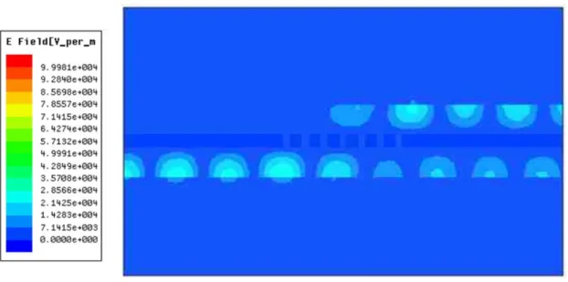
Figure 4-29: The TE20 mode is well contained in the guide when the side region is purely air. ... 92
Figure 4-30: The TE20 mode easily leaks into the side region if it is perforated. ... 92
Figure 4-31: Top view of a fabricated iSINRD cruciform coupler. ... 93
Figure 4-32: The simulated (S) and measured (M) results of the iSINRD cruciform coupler. ... 94
Figure 4-33: The simulated (S) and Measured (M) phase differences of the iSINRD cruciform coupler. ... 94
Figure 4-34: Top view of a fabricated asymmetric iSINRD cruciform magic-T. ... 95
Figure 4-35: The Simulated (S) and measured (M) results of the iSINRD cruciform magic-T. ... 96
Figure 4-36: The simulated (S) and measured (M) phase difference of the asymmetric iSINRD cruciform magic-T, relative to the ports 1 (in-phase) and 4 (out-of-phase). ... 96
Figure 4-38: The simulated (S) and measured (M) S-parameters for the LSM10 mode. ... 97
LIST OF SYMBOLS AND ABBREVIATIONS
ε1 Dielectric Constant of the Central Channel
ε2 Effective Permittivity of the Side Regions α Attenuation Constant
β Propagation Constant
λg Wavelength inside the Waveguide ALMA Atacama Large Millimeter-wave Array
C Calculated
CBCPW Conductor-Backed Co-Planar Waveguide.
CPW Coplanar Waveguide
E-band Frequencies in the range of 40 GHz to 65 GHz E-field Electric Field
EM Electromagnetic
fc Cut-off Frequency
fg Center Frequency
FHMSIW Folded Half Mode Substrate Integrated Waveguide
fn Minimum Operating Frequency
FSIW Folded Substrate Integrated Waveguide
fx Maximum Operating Frequency
H-field Magnetic Field
HFSS High Frequency Structure Simulator
HMSIW Half Mode Substrate Integrated Waveguide
IG Image Guide
iSINRD Image Substrate Integrated Non-Radiative Dielectric Waveguide iSIW Inverted Substrate Integrated Waveguide
K-band Frequencies in the range of 40 GHz to 65 GHz LSM Longitudinal Section Magnetic
LSE Longitudinal Section Electric LTCC Low Temperature Co-fired Ceramic
M Measured
MATLAB Matrix Laboratory
MHMIC Miniature Hybrid Microwave Integrated Circuits MOF Maximum Operating Frequency
NRD Non-Radiative Dielectric Guide
OMT Ortho-mode Transducer
PEC Perfect Electric Condition
PCB Printed Circuit Board
PMC Perfect Magnetic Condition PML Perfectly Matched Layer RF Radio Frequency
S Simulated
SIC Substrate Integrated Circuits
SINRD Substrate Integrated Non-Radiative Dielectric Guide SIIG Substrate Integrated Image Guide
SIW Substrate Integrated Waveguide
tanδ Loss Tangent
TM Transverse Magnetic
V band Frequencies in the range of 40 GHz to 65 GHz VNA Vector Network Analyzer
W band Frequencies in the range of 65 GHz to 110 GHz WR10 Rectangular Waveguide operating in the W-band X-band Frequencies in the range of 40 GHz to 65 GHz
LIST OF ANNEXES
ANNEX 1 – Field Equation of the and the Modes in the NRD Guide ... 114 ANNEX 2 – Field Plots for Circular-via iSINRD guide ... 117 ANNEX 3 – Field Plots for Square-via iSINRD guide ... 118 ANNEX 4 – Dielectric Loss in the iSINRD Guide ... 119
INTRODUCTION
Economic, compact, light, multifunctional and broadband, are but a few golden words that has been defining the evolution trend of telecommunication systems in recent decades. Coupled with the fact that technology in general is becoming increasingly ubiquitous and more readily available worldwide, meant that satisfying the aforementioned development trends ought to be on a large-scale, reproducible and reliable. In addition, access to higher frequency bands has proved to be a necessary requirement in order to satisfy increasing demand for bandwidth as well as frequency constraints some scientific applications have (e.g. the Atacama Large Millimeter-wave Array (ALMA) millimeter-wave astrophysics project [1]). To that end, classical system design approach requires a radical overhaul that continues to this very date, and this overhaul affects all stages of systems design, especially that pertaining to the design of RF circuitry.
The advent of WWII marked the real birthdate of RF and microwave communications systems. At that time, the state-of-the-art was circuits based mostly on the rectangular metal waveguide [2], [3]. While it is still vital for some contemporary applications such as conservative aerospace industry, it alone could not have accounted for the exponential technological growth of recent decades, as it fails to satisfy most of the trendy requirements mentioned above, especially low-cost, integration and compactness [4]. This has inspired researchers to develop more practical alternatives, such as the microstrip and the coplanar waveguide (CPW), which have proliferated the innovative circuits developed at the X band and other microwave ranges. At higher frequency bands, however, their loss performance degrades significantly, which has prompted the development of dielectric-based waveguides, such as the image [5] and the NRD-class guides [6–8]. All the above waveguides, however, share the same major challenge – seamless integration within the RF system as a whole in a manner that is amicable to mass production.
A new door to innovation was thus opened, with the substrate integrated circuits (SICs) design technology [9–11] taking center stage in the paradigm of RF circuits, thanks to its satisfaction of most, if not all, the modern trendy requirements. In the initial stages, the SICs technology facilitated seamless planar integration of the rectangular waveguide (thus called the substrate integrated waveguide or SIW) with other waveguide technologies [12–16]. Furthermore, it is scalable and flexible, as it supports single as well as multi-layer designs and can be realized with
different fabrication techniques such as PCB, MHMIC and LTCC. Consequently, the application portfolio of the EM spectrum witnessed an unprecedented growth, with the conception of a myriad of innovative K-band, and a couple of V- and E-band, SIW-based circuits (HMSIW, FSIW, FHMSIW, etc.) [17–27].
The design of SIW circuits, however, faces many limitations at bands higher than the Ka band. This is mainly because of the guide dimensions that approach fabrication tolerance with increasing frequencies; a characteristic problem of the rectangular waveguide [28]. In addition, the SIW does not support any TM mode, and it is limited predominantly to the TE10 mode. While
this could be an advantage, in the sense that mode conversion and interference is reduced, it nonetheless limits the full potential of the original rectangular waveguide for multi-mode applications. As a result, the scope of the SICs technology had to be expanded to include the image guide (IG) and the NRD guide. Generally speaking, the losses associated with dielectric guides could be much lower than the SIW counterparts, because less metal is involved. Furthermore, the dimensions of these guides are relatively above the fabrication tolerance, even at the W-band frequencies and beyond [28]. Therefore, the incorporation of these guides has proved to be a worthwhile initiative, as a number of novel V-band and W-band circuits based on the substrate integrated IG (SIIG) [28] and the substrate integrated NRD (SINRD) [29], [30] guides were recently reported. Unlike the SIW, the SINRD guide supports both the TM and TE (better known as LSM and LSE in the NRD literature) modes of the original NRD guide, and thus has deeper research potential. The SIW, SIIG and the SINRD guides are illustrated in Figure 1.
The NRD guide offers additional advantages over the IG; namely the electric symmetry of its dominant LSM10 mode and the orthogonality of LSM10 to the TE10 mode of the rectangular
waveguide (and the NRD guide, in which it can propagate at zero cut-off). Those advantages span two additional ones, namely doubled compactness and mode "quietness". These extra advantages are better manifested in the image NRD (iNRD) guide [31–33] shown in Figure 2; the vertical metal wall facilitating size reduction as well as suppression of several modes, especially the LSE10 mode, which may be considered unwanted in most cases. While both advantages are of
paramount significance, the latter is particularly worth mentioning because LSM10-LSE10 mode
conversion is inevitable in the design of NRD circuits with sharp corners [34–38], which limits the design of NRD circuits; unless otherwise required [39].
Figure 1 : Upper segment: exploded views of the rectangular waveguide (left), the NRD guide (centre) and the image guide (right). Lower segment: exploded views of the SIW (left), the SINRD guide (centre) and the SIIG (right). Orange: metal covers, black: metal vias, grey: insulating substrate of the SIIG, white: air vias, dark green: dielectric substrate which contains the waveguide.
Figure 2 : Cross-sectional front view of the E-field lines of the LSM10 mode in the SINRD guide
(left) and the image SINRD (iSINRD) guide (right).
In spite of the many advantages of the NRD and iNRD guides, they are not fully exploited in the literature. Furthermore, the iNRD guide is yet to be incorporated in the SICs design paradigm. It is thus envisioned that developing a substrate integrated iNRD (iSINRD) shall yield a multitude of innovative circuits with manifold advantages, especially at the W-band frequencies. This indeed is the objective of this thesis, with chapter 1 shedding more light on the proposed iSINRD and introducing a concise design scheme for the NRD-class waveguides, which is validated by practical implementations of iSINRD transmission lines in Chapter 2. Chapter 3 then highlights the aforementioned advantages of the iSINRD guide by implementing it in a number
of single-mode, multi-mode and dual-band directional coupler circuits.. The suppression of the LSE10 mode at sharp bends is highlighted in Chapter 4, which details the implementation of the
iSINRD guide in the design of four-port junctions such as cruciform couplers, cruciform magic-T, and ortho-mode transducer circuit circuits. The discussion then wraps up with concluding remarks and a future outlook.
Chapter 1 INVESTIGATION OF THE IMAGE SINRD GUIDE AT THE
W-BAND FREQUENCIES
1.1 Introduction
In the build-up to the implementation of the iNRD guide with the SICs technique, a theoretical discussion pertaining to the guide geometry and operating modes, alternative design methodology and procedure for selecting the guide parameters, as well as propagation and attenuation in the iSINRD guides, is carried out in the following sections. The alternative methodology discussed here is flexible in that it can be used for any perforation profile, although the discussion here focuses on the circular and square perforation profiles. It follows that a maximum of only two graphs is needed to design the iSINRD guide, although it involves at least triple the number of parameters of the original NRD guide; and if the substrate of effective permittivity is used instead of perforation, then only one graph is required.
1.2 Review of the NRD and SINRD Waveguides
1.2.1 Geometry of the NRD and SINRD Guides
The NRD waveguide, shown in Figure 1-1 (top, left), was first proposed in [6] as a low-loss waveguide that addressed the radiation-at-bends-and-discontinuities, which has been a well-known shortcoming of its H-guide predecessor [7], [8]; thus the name “non-radiative”. This is simply achieved by ensuring that the operating frequency is lower than fx; the cut-off frequency
of the 1st parallel-plate mode in the air side-regions (fg < fx; fx =
c 2
a
) [6]. So below fx, leakageinto the side regions due to bends and discontinuities is suppressed or contained [6]. Designing the NRD guide with the SICs technique yields the substrate integrated NRD (SINRD) guide [29], [30], which differs from the NRD guide by the fact that the side regions that flank the guiding channel are made of a lower permittivity dielectric (other than air). It naturally inherits all the features of the NRD guide, in addition to the SICs advantage of seamless integration with other planar circuitry. This dielectric contrast between the two regions can be done by perforating the substrate, less the NRD channel width, as per Figure 1-1 (top, right). In the rest of this work, the
lateral height and width of the guide are denoted by a and b, respectively; as shown in Figure 1-1 (bottom). Perforation is sometimes done with uniformly distributed non-metalized circular holes, but may not be limited to that, as shown in Figure 1-2. Obviously, there exist an infinite number of perforation profiles. The choice of a perforation profile depends on many factors such as the profile’s geometrical complexity, perforation impact on substrate’s fragility, practical feasibility with available fabrication tools, etc. The perforated regions have a lower effective permittivity compared to the ε1 of the middle channel. Perforation thus introduces more design variables, and
their number depends on the perforation techniques. For example, if perforation is done with circular via holes, then three new parameters are introduced: via diameter (D), the via-to-via spacing (gap) and the effective permittivity (εr2) of the perforated regions. The variable ε2,
anyhow, is always present in any SINRD guide design as it is a natural consequence of substrate perforation (regardless of the perforation technique). It is necessary for the calculation of fx =
2 2
/ a
c of the 1st parallel-plate mode in the perforated regions and β of the SINRD guide (see section 1.4.7). Sometimes, fx is called the maximum operating frequency (MOF) [29], [30],
because at fx, leakage into the side regions due to bends or discontinuities occurs. Hence, fx
designates the maximum frequency at which the SINRD guide can be operated; thus the name
MOF. In the rest of this work, fx is used to designate the MOF limit. It is essential to determine
the fx limit in order to design the SINRD for optimum performance. Note that the fx limit is
pertinent to the LSM10 mode discussed in the next subsection.
b ε 1 a Metal Air via Air via a/2 0 +b/2 -b/2 y +x -x V ia V ia ga p ga p V ia V ia
Figure 1-1: The NRD guide (top, left) and the SINRD guide (top, right). Bottom: Cross-sectional front view of the SINRD guide.
D gap p x w w gap g a p
Figure 1-2: Perforation Profiles (top view): circular profile (left), and square (right) perforation profiles; to name a few.
1.2.2 Dominant Modes
Another distinguishing feature of the NRD/SINRD guide is its multi-mode nature, as it supports four classes of hybrid symmetric and anti-symmetric (Hx = 0) and (Ex = 0)
modes. In this thesis, the mode nomenclature used in [6] is adopted, without loss of generality. It then follows that the dominant or fundamental modes of the NRD/SINRD guide are the symmetric (or LSM10), the symmetric (or TE10 in rectangular waveguide) and the
symmetric (or LSE10) modes. This mode richness expands the scope of the SICs design
paradigm to encompass more diverse applications such as the dual-polarized planar antenna arrays reported in [40], [41], and the H-guide antenna reported in [42], which operates with the mode. Cross-sectional front views of the three modes are shown in Figure 1-3. For other mode profiles, the interested reader is referred to [43], [44] and [45].
g a p g a p
v
ia
v
ia
g a pFigure 1-3: Cross-sectional front view of the E-field lines of the LSM10 (top), TE10 (bottom. right)
and LSE10 (bottom, left) modes in the (SI)NRD guide. Encircled × (into page) or · (out of page)
The field equations for each mode are given by the equations below, where regions 1 and 2 refer to the central guiding channel and the perforated side regions, respectively [43]. It can be deduced from those equations that the three dominant modes are mutually quasi-orthogonal [39], [46]. Furthermore, it is important to note the E-field of the LSM10 mode has all three components,
and that the Ez component is maximum at the interface between guiding channel and the
perforation region (x = b/2), and null at the centre (x = 0). This is property of the Ez component is
fundamental to the design of many circuits in the subsequent chapters. The general field equations of symmetric and asymmetric and modes are given in Annex 1. In the remaining discussion, the three modes presented in this sub-section are referred to as LSM10,
LSE10, and TE10, respectively.
Symmetric (or LSM10) Mode
( | ⁄ |) . ( ⁄ ) ( ⁄ ) ( ) (1.1 a) ( ⁄ )( ) ( ⁄ ⁄ ) ( ) (1.1 b) ( ⁄ ) ( ⁄ ) ( ) (1.1 c) (1.1 d) ( ⁄ ) ( ) (1.1 e) ( ) ( ⁄ ⁄ ) ( ) (1.1 f) ( | ⁄ |) . ( ⁄ ) ( ⁄ ) ( | |)⁄ (1.1 g) ( ) ( ⁄ ⁄ ) ( ⁄ ) ( | |)⁄ (1.1 h) ( ⁄ ) ( ⁄ ) ( | |)⁄ (1.1 i) (1.1 j) ( ⁄ ) ( ⁄ ) ( | |)⁄ (1.1 k) ( ) ( ⁄ ⁄ ) ( ⁄ ) ( | |)⁄ (1.1 l)
Symmetric (or LSE10) Mode ( | ⁄ |) . (1.2 a) ( ⁄ ) ( ) (1.2 b) ( ⁄ ) ( ⁄ ) ( ) (1.2 c) ( ⁄ ) ( ) (1.2 d) ( ⁄ ) ( ⁄ ) ( ) (1.2 e) ( ⁄ ) ( ) (1.2 f) ( | ⁄ |) . (1.2 g) ( ⁄ ) ( ⁄ ) ( | |⁄ ) (1.2 h) ( ⁄ ) ( ⁄ ) ( ⁄ ) ( | |)⁄ (1.2 i) ( ⁄ ) ( ⁄ ) ( | |)⁄ (1.2 j) ( ⁄ ) ( ⁄ ) ( ⁄ ) ( | |)⁄ (1.2 k) ( ⁄ ) ( ⁄ ) ( | |)⁄ (1.2 l)
Symmetric (or TE10) Mode
( | ⁄ |) . (1.3 a) ( ) (1.3 b) (1.3 c) ( ) (1.3 d) (1.3 e)
( ) (1.3 f) ( | ⁄ |) . (1.3 g) ( ⁄ ) ( | |⁄ ) (1.3 h) (1.3 i) ( ⁄ ) ( | |)⁄ (1.3 j) (1.3 k) ( ⁄ ) ( | |)⁄ (1.3 l)
In all of the above equations, p and q are related by the following relationship:
( )⁄ (1.4)
where β is the propagation constant in the waveguide, m is the order of the mode (1 for the LSM10
and LSE10 modes; 0 for the TE10), ε1 is the permittivity of the substrate, ε2 is the effective
permittivity of the perforated regions, βx is the transverse propagation constant in the dielectric,
and φ is the attenuation constant in the perforated region. While the cut-off frequency of the TE10
mode is zero [43], that of the LSM10 mode can be deduced from equation 1.5, by matching the E
components at the air-dielectric interface. Cut-off of the LSE10, and other, modes is give in [43].
( ⁄ ) (1.5 a)
( ⁄ ) ( ⁄ ) (1.5 b)
1.3 Design Challenges of the SINRD Guide
Although perforation simplifies the physical fabrication of the SINRD guide, it nonetheless limits the application scope of the SINRD guide since the perforated regions are strictly reserved for the air vias, and increase the total width of the guide to more than twice that of the guiding channel (width b). Furthermore, it complicates its theoretical design since any perforation profile will entail additional design parameters that must be accurately identified for operation at a desired fg; a problem that is not treated in-depth in the SINRD literature.
The design method of SINRD guide circuits is not so straightforward. This is attributed to the lack of an accurate justification of the optimum dimensions for a desired frequency of operation, henceforth called fg. Specifically, the fx limit is insufficient for precisely determining the
thickness a (and thus width b) of the guide. For the SINRD and iSINRD guides, the situation is further complicated because of the additional perforation variables that are difficult to inter-relate with the lateral dimensions. It is thus imperative to accurately determine all those parameters in order to obtain a correct operation at the desired operating frequency, fg, and operating mode.
Some effort has been made at relating those many variables [47], but they are incomplete and rather vague, with insufficient explanation of how the lateral dimensions (a and b), and the perforation geometry should be selected. Furthermore, the analysis in [47] is limited to a few variations of the circular perforation profile, and does not consider the general case. Also, the existing relations for calculating ε2 [30] do not take into account the variations of ε2 with
frequency reported by [48], [49].
In the next section, the first problem is mitigated by implementing a metal image plane at the center of the guide which reduces the total size by 50%, and does away with one of the perforated regions. For the second problem, a new (missing) design limit that should supplements the fx limit
is introduced, and will substantially improve the way in which the dimensions of SINRD circuits are chosen. Then, a concise and clear method for determining all pertinent dimensions is presented. As will be shown, this approach is versatile in the sense that it is applicable to any perforation profile. Only a couple of extra steps are required for the SINRD guide. For the iSINRD guide, one further "step" is required, which is simply halving the value of width b! Prior to that, a fast, accurate and novel analysis approach is proposed that substantially simplifies the analysis and accurately characterizes the SINRD guide.
1.4 Proposed Alternative Design Approach of the SINRD Guide
1.4.1 The Image SINRD (iSINRD) Guide
The mode diversity discussed above can equally be a nuisance for some applications as mode conversion may take place, especially between the LSE10 and LSM10 modes and also along
waveguide bends, as mentioned above. Mode suppressors would then be needed to suppress one of the two modes [47], [50].
Looking at the H-field of the LSM10 mode in Figure 1-3, it has a vertical electric symmetry.
Based on the image theory, bisecting the NRD guide with a vertical longitudinal metal wall yields the image NRD (iNRD) guide [31–33], which supports the propagation of the LSM10
mode; as shown in Figure 1-4. Conversely, the LSE10 and the TE10 modes are suppressed. In fact,
all symmetric modes are consequently suppressed [31]. This situation is advantageous for applications that rely solely on the LSM10 mode, and/or waveguide bends, since LSE10-LSM10
mode conversion can safely be ignored. The iNRD guide is thus a very simple LSE10 mode
suppressor.
Other than the LSM10, the iNRD guide also supports the asymmetric (TE20 in rectangular
waveguide) mode, which is shown in Figure 1-4. This fact is utilized to design a set of multimode planar circuits; as shall be shown in Chapter 3. Similar to the LSM10 mode, the mode is
hitherto called the TE20 mode.
a
b/2
v
ia
g
a
p
v
ia
a
b/2
v
ia
g
a
p
v
ia
Figure 1-4: The cross-sectional front view of the E-field lines of the LSM10 (left) and TE20 (right)
modes in the iSINRD guide.
Asymmetric (or TE20) Mode ( | ⁄ |) . (1.6 a) ( ) (1.6 b) (1.6 c) ( ) (1.6 d) (1.6 e) ( ) (1.6 f) ( | ⁄ |) . (1.6 g) ( ⁄ ) ( | |⁄ ) (1.6 h) (1.6 i) ( ⁄ ) ( | |)⁄ (1.6 j) (1.6 k) ( ⁄ ) ( | |)⁄ (1.6 l)
The cut-off of the TE20 mode is obtained by matching the Hz components at the air-dielectric
interface. Re-arranging equation 1.6 and setting m = 0, yields the following conditions:
(1.7 a)
( ⁄ ) (1.7 b)
Besides the mode suppression, the iSINRD guide offers an additional advantage over the SINRD guide; namely size compactness, since the iSINRD guide is half the size of the SINRD guide. The iSINRD guide is thus an optimum choice between the SINRD guide and the SIW. Nonetheless, it is yet to be reported in the SINRD literature. Thus, the objective of this thesis is to exploit the rich potential of the iNRD guide in the SICs paradigm; i.e. the iSINRD guide. Prior to that, however, an optimisation of the design approach of the SINRD circuits is worthwhile, which is detailed in the next section. Unless otherwise stated, it must be emphasized that the following discussion focuses on the LSM10 mode, since the iSINRD guide is the cornerstone of this thesis.
1.4.2 Eigen-Mode Analysis of Periodic SINRD Guides
Full-wave analysis of periodic general NRD-class guides, such as the SINRD guide, is expensive in terms of computational time and resources. This fact is manifested when computing the cut-off frequency and the propagation curve of the LSM10 mode, especially when the side
regions are not air and the effective permittivity is unknown a priori. Alternatively, the guide should be analysed with a 3D Eigen-mode technique that is available in well-known microwave solvers such as [51], [52]. Floquet’s theorem [44] is the underlying principle of Eigen-mode analysis for periodic structures. In brief, in a periodic structure, the electromagnetic fields at point
x differ from those at point x + p, by only eγp where p is the period of the structure [44]. Obviously, this requires the guide, and thus the perforation profile, to be periodic. Then, only a “unit-cell” of the guide needs to be analysed. Consequently, the computational time and resources needed for the analysis are reduced enormously. Furthermore, the values of the cut-off frequency,
fc, and the propagation constant, β, that are obtained with this technique are more accurate
because the analysis is done inside the guide, instead of relative to the wave-port in a full-wave analysis. With this technique, many essential parameters can be extracted, such as the propagation and attenuation constants (β and α). For the iSINRD guide, only half the SINRD guide needs to be studied, as shown in Figure 1-5. To simulate the open end of the iSINRD, a perfectly matched layer (PML) boundary condition should be applied at the edge of the unit cell. By default, perfect electric conductor (PEC) is assigned to the top and bottom planes. Note that the vias are also covered with metal, but are not metallized from the inside. To further enhance the efficiency, the perforated region can be replaced with an equivalent ε2-dielectric. The value of
ε2 may not be initially known, in which case it will be determined based on the desired cut-off
frequency as well as the feasibility of a corresponding perforation profile. The advantages of the Eigen mode solver are further highlighted in [101].
z
x
y
Figure 1-5: A 3-D view of a unit-cell of the iSINRD waveguide in HFSS Eigen-mode solver together with a cross-sectional front view of the simulated E-field of the LSM10 mode.
1.4.3 The SINRD Guide as a Generalised NRD Guide
The best way to approach the design of an SINRD guide is to visualize it as a generalized NRD waveguide with the side regions filled with an arbitrary dielectric material (1 < ε2 < ε1). This
simplifies the discussion substantially. The ε2-dielectric is an abstract representation of the
perforated regions. Hence, regardless of what the perforation profile is, the designer needs only to look at the resultant ε2; hereby reducing the design complexity to only three variables (a, b, and
ε2). Relating the ε2 to the dimensions of the perforation profile is then left as a last step, which
varies depending on the perforation profile. Figure 1-6 illustrates a cross-sectional view of this visualisation.
The choice of dielectric substrate suitable for the W-band applications is very tricky because not many materials maintain low loss tangent (tanδ) characteristics over a wide frequency range. Several studies confirm that the tanδ of many polymer (e.g. Teflon ε1 = 2.06, tanδ = 0.00024 and
Polystyrene ε1 = 2.53, tanδ = 0.0007) and ceramic substrates (such as Alumina ε1 = 9.8, tanδ =
0.00015) up to 110 GHz is on the order of 10-4 [45], [53–59], which is roughly ten times less than its Rogers counterparts (e.g. RO6010) even at 10 GHz [60]. For the design of SINRD circuits, other factors should also be considered. For optimal wave guidance in the central channel,
dielectric guides in general are typically designed with a high permittivity (ε1 > 9) dielectric
material [61]
.
This is because waves in such waveguides are primarily surface waves, and hence a higher dielectric contrast between the dielectric and the surrounding medium correspond to better attenuation of the field in the surrounding; i.e. waves are more confined in the central dielectric [61]. Therefore, Alumina is chosen in the rest of this work. The discussion in the following subsection confirms this choice. Table 1.1 presents a comparison between a numbers of dielectric material candidates with which an iSINRD guide can be realised. For the sake of certainty, the loss tangent of Alumina was measured at our lab at 94 GHz and the measured value indeed conforms with the one cited in [59].a
b
ε
2ε
1ε
2 Figure 1-6: The cross-sectional front view of a generalised NRD guide.Table 1.1: Comparison of different dielectric materials at different millimeter-wave frequencies.
Material Frequency (GHz) εr tanδ (×10-4) Reference
Teflon 100 2.06 2.4 [53–59]
Polyethylene 100 2.53 0.7 [53–59]
Alumina 94 9.8 1.5 [59]; measured
RO6010 10 10.2 23 [60]
1.4.4 The Minimum Operating Frequency, f
nand the Choice of Thickness a
For any given a, b can theoretically assume any value in the abstract range [0:∞]. If b = 0, then the structure is a parallel-plate waveguide filled with a ε2-dielectric, whose 1st mode cut-off
frequency is
fc1=c (2a 2) (1.8)
Equation 1.8 is the fx limit discussed in Section 1.2. Since this is the maximum operating
frequency of the general NRD guide, then, for b > 0, the structure becomes an NRD guide whose
fg < fx; a rather obvious result. Now, if b is continuously increased to b = ∞, then the structure is
again a parallel-plate waveguide, filled with a ε1-dielectric material, whose 1st mode cut-off
frequency is
fc1 = fn=c(2a 1) (1.9)
Since fn can only be obtained for b = ∞, and is independent of ε2, then it is intuitive to conclude
that operation below this frequency is impossible for 0 < b < ∞. Hence, fn is the “minimum
operating frequency” at which the NRD guide can operate. This is the supplementary limit mentioned at the end of the previous section. Since both fx and fn depend on a, each value of a
corresponds to a distinct set of fx - fn limits or operating frequency bands (fg -bands), as shown in
Figure 1-7. Thus, varying a in the range [0:∞] results in a super-band of fg-bands. At the lower
part of the spectrum, the bands strongly overlap, and the choice of a is no longer critical; i.e. the super-band saturates at lower frequencies. This scenario is reversed at the upper part of the spectrum. Hence, a should be chosen such that it corresponds to an fg-band that covers the desired
Figure 1-7: Frequency fx-fn bands corresponding to different thicknesses computed with [62].
1.4.5 Determining the Optimum Thickness a
The significance of the fn limit is subtle yet crucial, as without the fn limit, one can be misled
into thinking that operating at any fg < fx is possible for a given thickness. It is therefore important
to supplement the fx limit with this new fn limit. This scenario is illustrated in Figure 1-8. Note
that as ε2 approaches ε1, the fx and fn limits converge to the same single point. This point is
another way of visualising a channel width b equal to infinity; except that no substrate perforation is performed.
The choice of thickness a should be such that the desired fg is not close to either fx or fn, as
unrealistic values of channel width b would be required (close to zero or infinity). For small increments of a (typically, ∆a = 5 mil), the decision should be made based on which band corresponds to the maximum number of ε2 values for the desired fg. This is to ensure design
flexibility and robustness. That is, a wider range of ε2 values gives more flexibility in choosing
Figure 1-8: Comparison of two operation bands: a/λg = 0.381 and a/λg = 0.635. Operation at 94
GHz with a/λg = 0.381 using Alumina is impossible.
The above analysis is valid for any dielectric material and for any thickness. In fact, any particular fg-band can be obtained with different ε1-dielectrics by adjusting their respective
thicknesses, a; as per Figure 1-10. Obviously, for the same fg-band, higher fx, (and thus fg and
bandwidth) values can be attained with high ε1 dielectrics, since a smaller ε2/ε1 contrast ratio can
be theoretically conceived compared to the dielectrics with smaller ε1. This verifies the
observation in [43] that high ε1 substrates yield considerably larger bandwidth. Furthermore,
compared to low ε1 dielectrics, high ε1 dielectrics require a smaller thickness “a” to obtain the
same fg-band; which is in-line with the miniaturization trend of RF circuits. In light of the above,
the optimum substrate and its thickness, for the W-band, are Alumina and a/λg = 0.635,
respectively. r2 1 ε 1 2 , 1 , fn
Operation below impossible Operation above fx impossible
Limit of the RO 3006 band, ( NRD, ε 2 = 1)
Limit of Alumina band (NRD, ε 2= )1
ε Limit of the RO5880 band ( NRD , = )
= ) Pure Parallel plate, 2 = ε
f
n< f
g< f
xFigure 1-10: Different dielectrics with unequal thicknesses corresponding to the same fg-band.
1.4.6 Determining channel width, b and effective permittivity ε
2Intuitively, each fg-band should in turn contain operation curves for different values of b, as
shown in Figure 1-11 for Alumina (ε1 = 9.8) with a/λg = 0.635. Ideally, minimizing ε2 is desired as
fragility. Conversely, high values of ε2 reflect very little perforation and thus higher susceptibility
to leakage. As a compromise, ε2/ε1 = 0.5. According to Figure 1-12, this corresponds to b = 0.826
λg. In terms of bandwidth (%∆f), these values correspond to a 16.5% bandwidth, as per
Figure 1-13. The bandwidth is calculated using:
%∆f = [(fx - fc, LSM10)/fg] ×100% (1.10)
The choice of ε2/ε1 = 0.5 is further justified in the next subsection.
Figure 1-11: Operation curves, within an fg-band, for different values of the width, b, and for a
Figure 1-12: Choosing the width, b, based on the desired
ε
r2/ε
r1 ratio operating frequency, fg.1.4.7 Relating ε
2to Perforation Dimensions
The remaining task now is to choose the perforation profile. Typically, factors such as fabrication feasibility and performance significantly influence the decision. On one hand, at our lab, the most feasible perforation profile is the periodic circular-via profile. On the other hand, a square-via perforation profile models the original NRD/iNRD guide more closely (since the only difference would be the periodic inter-via gaps). Hence, a trade-off is needed that would depend on the target application and/or the performance parameter being investigated. Figure 1-14 and Figure 1-15 display the relationship between the ratio ε2/ε1 and the period p of circular-via and
square-via unit-cells, respectively, for different values of gap. These relationships were obtained by simulating, for different gap values, a set of SINRD guide unit-cells with different p values, and a set of general NRD guides for different ε2/ε1 ratios, and then comparing their dispersion
curves. Then, if the dispersion curves of a generalized NRD guide with ε2/ε1 = x, and an SINRD
guide with p = y, gap = z, are identical, it means that the two are identical waveguides. For example, in Figure 1-14, a circular-via perforation profile with D/λg = 0.508, gap/λg = 0.254 (i.e.
p/λg = 0.762) results in ε2/ε1 = 0.5 as selected above; i.e. almost 50% substrate perforation.
Similarly, in Figure 1-15, a square-via perforation profile with w/λg = 0.55, gap/λg = 0.254 (i.e.
p/λg = 0.8) would be needed to obtain the desired ε2/ε1 = 0.5 ratio. In fact, these are roughly the
“safe” fabrication limits at our lab [63].
To conclude, this section provides an efficient way of choosing the optimum dimensions of the SINRD guide. Specifically, at 94 GHz using Alumina, and circular-via perforation, its dimensions are: a/λg = 0.635, b/λg = 0.826, D/λg = 0.508, and gap/λg = 0.254, respectively;
corresponding to fc = 84 GHz, and fx = 102.5 GHz. Alternatively, the same performance can be
achieved with a square-via perforation that differs from the circular counterpart only in the dimension of the square-via. In the case of the iSINRD guide, the width is bi = b/2λg = 0.413.
Unless otherwise specified, those dimensions shall be used in the entirety of this thesis.
Field plots for both profiles at fc, fg, and fx are shown in the Appendix B. Figure 1-16 verifies
that the NRD, iSINRD and SINRD guides are identical, by plotting the dispersion curve of the
LSM10 mode, obtained with the Eigen-mode solver using the equation (where ϕ and Δl are the
l
(1.11)
The calculated dispersion curve of the generalised NRD guide is also included and is identical to the simulated ones. It was obtained by solving equation 1.5 above [64]. Also included in Figure 1-16 is the propagation curve for the TE20 mode, obtained by solving the equation 1.7
above. It is clear that the cut-off of the TE20 mode in the NRD guide differs from that in the
rectangular waveguide [48].
It must be mentioned that while the value of the width b deduced in the above discussion is the optimum for the desired fg, other values can still be used. This is not a contradiction, given the
fact that a specific value of b also corresponds to a bandwidth of frequencies, and thus any b value can well correspond to the desired fg. The optimum value in this context refers to a value of
b that results in a bandwidth centered at fg. A non-optimum value of b then corresponds to a
bandwidth that includes fg but is centered at another frequency. This explains the reason behind
using the term operating frequency instead of center frequency.
D gap
p
xx x gap g a p w w
Figure 1-15: Relating εr2/εr1 to p/λg (p = gap + w) for the square-via profile.