HAL Id: tel-02320246
https://tel.archives-ouvertes.fr/tel-02320246
Submitted on 18 Oct 2019HAL is a multi-disciplinary open access archive for the deposit and dissemination of sci-entific research documents, whether they are pub-lished or not. The documents may come from teaching and research institutions in France or abroad, or from public or private research centers.
L’archive ouverte pluridisciplinaire HAL, est destinée au dépôt et à la diffusion de documents scientifiques de niveau recherche, publiés ou non, émanant des établissements d’enseignement et de recherche français ou étrangers, des laboratoires publics ou privés.
oscillator
Alice Bernard
To cite this version:
Alice Bernard. Towards an electrically-injected optical parametric oscillator. Physics [physics]. Uni-versité Sorbonne Paris Cité, 2018. English. �NNT : 2018USPCC104�. �tel-02320246�
THESE DE DOCTORAT DE L’UNIVERSITE
SORBONNE PARIS CITE
PREPAREE A L’UNIVERSITE PARIS DIDEROT – PARIS 7
ECOLE DOCTORALE 564 : PHYSIQUE EN ILE-DE-FRANCE
LABORATOIRE MATERIAUX ET PHENOMENES QUANTIQUES
Towards an electrically
injected optical parametric oscillator
Par Alice BERNARD
Thèse de doctorat de physique
Dirigée par Giuseppe LEO
Présentée et soutenue publiquement à Paris le 10 juillet
2018
Présidente du jury : Mme Angela VASANELLI
(Université Paris 7)
Rapporteurs : Mme Isabelle SAGNES
et M. Laurent VIVIEN (C2N)
Examinateurs : M. Claudio CORIASSO (Prima Electro)
et M. Claude ALIBERT (Université de Montpellier)
Directeur de thèse : M. Giuseppe LEO (Université Paris 7)
Co-directeur de thèse : M. Jean-Michel GERARD (CEA)
Membre invité : M. Michel KRAKOWSKI (III-V Lab)
Remerciements
Mon travail s’est partagé entre deux centres de recherche, l’Université Paris 7 et le Commissariat à l’Energie Atomique. Je garde de ces deux endroits un excellent souvenir. Même si je remercie ici une poignée de gens, ce sont toutes les personnes avec qui j’ai interagi pendant la thèse qui m’ont fourni un environnement de travail optimal. Je souhaite également saluer l’UFR de Physique de Paris 7 pour la qualité des cours proposés, en particulier aux étudiants de première année, me donnant envie de continuer dans le domaine.
Je remercie mon directeur de thèse de m’avoir fait confiance pour porter un projet ambitieux et de m’avoir donné beaucoup de liberté. Giuseppe m’a fourni un environnement de travail stimulant, s’est toujours montré dynamique et motivé, et m’a donné beaucoup de temps, d’enthousiasme et de bonnes idées. Je remercie aussi Jean-Michel pour sa gentillesse, son calme, sa créativité, sa disponibilité constante et sa capacité infinie à résoudre les problèmes pratiques et théoriques. Merci également à mes rapporteurs, Laurent Vivien et Isabelle Sagnes, pour l’attention détaillée portée à mon manuscrit et pour leurs suggestions, ainsi qu’aux membres de mon jury, Claudio Coriasso, Claude Alibert, Michel Krakowski et Angela Vasanelli. Merci aussi à Philippe Adam, qui a montré un intérêt constant envers le projet et m’a aussi fait confiance pour le mener à bien.
Avant et pendant la thèse, il y a beaucoup de personnes que je voudrais remercier : merci donc à Sara Ducci pour l’intérêt des cours de son master et pour avoir été toujours présente pour orienter mes amis ou moi, et à Maria Amanti de m’avoir encadrée sur mes premières manips, de m’avoir donné la première occasion d’être co-auteur sur un article et de m’avoir conseillée par la suite. A Julien Claudon et Joël Bleuze, merci de leur gentillesse, leur culture scientifique et d’avoir toujours la porte ouverte pour une discussion. Je remercie aussi Yann Genuist pour ses exploits quotidiens avec la MBE et Yoann Curé pour ses coups de pouce avec la PL ou l’informatique. Merci à Alessio Andronico pour les outils développés et sa bonne humeur, à Marco Ravaro pour ses mesures et suggestions, à Yohan Désières pour ses conseils avisés, à Badhise Ben Bakir pour des discussions stimulantes, et à Jean-Luc Rouvière et Edith Bellet-Amalric pour avoir caractérisé mes échantillons avec talent. Je souhaite aussi remercier les doctorants et post-doctorants pour leur accueil, en particulier Cécile Ozanam et Silvia Mariani. Merci à William Hease
d’avoir été toujours disponible pour débattre passionnément de fabrication en salle blanche, même depuis l’Autriche, et à Tiphaine Dupont d’avoir pris une soirée pour me parler de l’intégration III/V sur Si. Merci à Romain Fons d’avoir pris la relève pour les derniers échantillons, et à Tobias Sattler et Alberto Artioli pour les blagues et les longues conversations. Pour les échanges de matériel, les discussions et la bonne humeur, je remercie Fares, Biswarup, Mehdi, Natalia, Valerio, Pierre, Eduardo, Debora, Samanta, Carlo, Iannis, Daria, Yacine, Guillaume, Claire et les autres. Je remercie aussi les permanents, qui nous prêtent du matériel et facilitent notre quotidien : Ivan Favero, Régis André, Moïra Hocevar, Eva Monroy, Bruno Gayral, Christophe Durand, Joël Eymery, Henri Mariette, Joël Cibert, Jean-Phillipe Poizat, Bruno Daudin, Didier Boilot…
Je tiens aussi à saluer les ingénieurs de salle blanche, qui tiennent une place centrale dans notre travail. Merci donc à Stephan Suffit pour son humour et pour m’avoir formée au top niveau du MEB, ainsi qu’à Christophe Manquest et Pascal Filloux. Côté PTA, je n’aurais jamais pu réaliser les structures de cette thèse sans l’aide de Thierry Chevolleau et Thomas Charvolin, que je remercie chaleureusement. Merci également à Jean-Luc Thomassin de m’avoir débloquée de nombreuses fois pendant des lithographies, ainsi qu’à Marlène Terrier, Christophe Lemonias, Nicolas Chaix, Frédéric Gustavo, Michaël Rosticher et Loïc Becerra.
Je remercie aussi le personnel administratif pour leur efficacité et leur sympathie : Joëlle Mercier, Jocelyne Moreau, Anne Servouze et Céline Conche. Côté électronique et mécanique, merci à Marc Apfel, Alain Cangemi, Patrick Lepert et Martial Nicolas pour leur compétence et leur gentillesse.
Je remercie chaleureusement Michel Krakowski pour sa disponibilité et son efficacité, ainsi que Bruno Gérard et Olivier Parillaud pour leur place capitale dans ce projet.
Finalement, merci aux amis et à la famille, en particulier Vincent pour son humour, Mathias pour avoir fait disparaître les problèmes pendant la soutenance et avant, et Pedro pour son soutien constant. Et naturellement, mes parents pour tout.
Contents
List of figures vii
List of tables xii
List of acronyms xiii
Introduction 1
1. Three-wave mixing in GaAs 11
1.1 Nonlinear optics in plane waves ... 11
1.1.1 From the nonlinear polarization to the coupled equations ... 11
1.1.2 Three-wave mixing processes ... 13
1.1.3 Second-harmonic generation ... 14
1.1.4 Optical parametric amplification ... 16
1.2 Nonlinear optics in waveguides ... 17
1.2.1 Effective area ... 17
1.2.2 SHG in the presence of losses ... 18
1.2.3 OPA in the presence of losses ... 20
1.2.4 OPA in the presence of gain... 21
1.3 OPOs ... 22
1.3.1 Single pass DROPO ... 23
1.3.2 Double-pass DROPO ... 25
1.3.3 TROPO ... 27
1.4 Phase-matching strategies in GaAs ... 33
1.4.1 Form birefringence ... 34
1.4.2 Quasi-phase matching ... 35
1.4.3 Modal phase matching ... 37
2. QD and QW laser diodes 41 2.1 Phenomenological description of lasers ... 41
2.1.1 Optical gain in a two-level system ... 41
2.1.2 Laser threshold condition ... 42
2.1.3 Loss sources ... 45
2.1.4 Efficiency ... 46
2.2 Gain in semiconductors ... 48
2.2.1 Fermi Golden Rule ... 49
2.2.2 Bulk case ... 50
2.2.3 Quantum wells ... 53
2.2.4 Quantum dots ... 55
2.3 Optical selection rules ... 59
3. Diode-OPO: concept and design 63 3.1 Phase-matching bandwidth and quantum dots laser spectrum ... 64
3.2 Choice of epitaxial structure ... 66
3.2.1 Refractive index model ... 66
3.2.2 Phase matching ... 67
3.2.3 Modal selection ... 70
3.2.4 Phase-matching tolerances ... 74
3.3 Choice of the doping profile ... 76
3.3.1 Doping profiles in the GaAs-based diode ... 77
3.3.2 Doping profiles in the InP-based diode ... 79
3.3.3 Modal gain necessary for laser threshold ... 81
3.3.4 Threshold current ... 82
3.3.5 Additional loss sources for signal and idler ... 84
3.4 Conclusion ... 85
4. Laser characterizations 87 4.1 Optical setup ... 87
4.2 Basic characteristics ... 88
4.3 Far field measurements ... 91
4.5 Effect of trapped carriers outside the camelback ... 95
4.6 Conclusion ... 96
5. Refractive index measurements 99 5.1 Justification ... 99
5.2 Principle of measurement ... 99
5.3 Sample fabrication and characterization ... 101
5.3.1 Growth ... 101
5.3.2 Composition measurement ... 101
5.3.3 Choice of grating period ... 103
5.3.4 Gratings fabrication ... 103 5.4 Measurement ... 105 5.4.1 Optical setup ... 105 5.4.2 Measurement procedure ... 106 5.5 Results ... 108 5.6 Discussion ... 110 5.6.1 Experimental accuracy ... 110
5.6.2 Comparison with literature ... 112
5.7 Conclusion ... 113
6. Fabrication 115 6.1 Fabrication overview of ridge lasers ... 115
6.2 Choice of etch mask... 116
6.3 Optical lithography ... 116 6.4 Mask roughness ... 120 6.5 ICP-RIE etching ... 121 6.5.1 Requirements ... 121 6.5.2 Principle ... 123 6.5.3 Etching mechanisms ... 124 6.5.4 Choice of chemistry ... 125 6.5.5 Results ... 125
6.5.6 Choice of parameters ... 127
6.5.7 Passivation layer ... 129
6.6 Removal of mask residues ... 129
7. Double-cavity DOPO 133 7.1 Choice of coupling method ... 133
7.1.1 Evanescent couplers ... 134
7.1.2 Bragg-exchange ... 135
7.1.3 Adiabatic couplers ... 135
7.1.4 Adiabatic couplers physics in a nutshell ... 137
7.2 Critical points ... 139
7.3 Choice of geometry ... 140
7.4 Proposed design ... 140
7.4.1 Choice of material ... 142
7.4.2 Conversion efficiency and OPO threshold ... 143
7.4.3 Tolerances ... 144 7.4.4 DBR design ... 146 7.4.5 Tunability ... 146 7.4.6 Transfer ... 147 7.4.7 Laser ... 152 7.5 Conclusion ... 154 General conclusion 146 List of publications 149 Bibliography 150
Résumé
Le travail présenté dans cette thèse porte sur la conception, la fabrication et la caractérisation de sources prévues pour fonctionner à la fois comme diode laser et comme oscillateur paramétrique optique. Ces lasers sont conçus pour émettre sur un mode d’ordre supérieur afin de permettre une conversion de fréquence paramétrique avec les modes fondamentaux du guide à la fréquence moitié. La diode laser et l’OPO partagent la même cavité optique ; pour assurer l’accord de phase et corriger les écarts à la structure nominale induits lors de l’élaboration par épitaxie, la largeur de ruban est utilisée comme paramètre de contrôle des indices efficaces. Les diodes proposées sont donc étroites (3-5 µm) et gravées profondément. En conséquence, il est potentiellement intéressant d’utiliser des boîtes quantiques pour limiter les recombinaisons non radiatives sur les flancs.
Dans le cadre de ce travail, nous avons conçu des diodes basées sur ce principe pour les deux systèmes GaAs/AlGaAs et InGaAsP/InP, qui permettent respectivement d’obtenir potentiellement une émission OPO au voisinage de 2 µm ou de 3 µm. Dans le cas de l’InGaAsP/InP, nous avons étudié au préalable l’indice de réfraction des alliages InGaAsP dans une plage de longueur d’onde jusque-là non couverte par la littérature. Ces données ont été acquises via des mesures d’indice efficace (m-lines) de couches guidantes d’InGaAsP épitaxiées en accord de maille sur un substrat d’InP. Pour des structures laser-OPO optimisées, les simulations montrent que le seuil OPO devrait être obtenu pour une puissance de pompe intracavité de quelques centaines de mW, qu’il est réaliste d’atteindre pour des diodes laser à l’état de l’art. Nous avons étudié les propriétés électro-optiques de diodes lasers à puits quantiques GaAs/AlGaAs réalisées sur la base de nos dessins; l’observation de l’effet laser sur le mode TE2 valide le dessin vertical original de nos diodes lasers. En vue de la fabrication de laser-OPO à ruban étroit, nous avons développé des procédés de fabrication nouveaux sur la Plateforme Technologique Amont (CEA – Grenoble), notamment la gravure profonde (>10 µm) par ICP-RIE. Enfin, nous avons proposé un concept alternatif de diode-OPO, comprenant des cavités laser et OPO distinctes couplées par un taper adiabatique.
Mots-clés: diode laser, Fabry-Pérot, Oscillateur Paramétrique Optique, épitaxie par
jet moléculaire, guide d’onde, photonique intégrée, AlGaAs, InGaAsP, boîtes quantiques, puits quantiques, mesures d’indice efficace, gravures par ICP-RIE.
Abstract
The work presented in this thesis deals with the design, fabrication and characterization of sources intended to function as both laser diodes and optical parametric oscillators. These lasers are designed to emit on a higher order mode to allow parametric frequency conversion with fundamental modes of the guide at half frequency. The laser diode and OPO share the same optical cavity; to ensure phase matching and correct nominal structure deviations induced during epitaxial processing, the ridge width is used as a control parameter of the effective indices. The proposed diodes are therefore narrow (3-5 µm) and etched deeply. Consequently, it is potentially interesting to use quantum dots to limit non-radiative recombination on the sidewalls.
In the context of this work, we have designed diodes based on this principle for the two GaAs/AlGaAs and InGaAsP/InP systems, which respectively allow to potentially obtain an OPO emission in the vicinity of 2 µm or 3 µm. In the case of InGaAsP/InP, we previously studied the refractive index of InGaAsP alloys in a wavelength range not covered by literature to this day. This data was acquired via effective m-line index measurements of InGaAsP guiding layers epitaxially grown on and lattice-matched to an InP substrate. For optimized laser-OPO structures, simulations show that the OPO threshold should be obtained for an intracavity pump power of a few hundred mW, which is realistic to achieve for state-of-the-art laser diodes. We have studied the electro-optical properties of GaAs/AlGaAs quantum well laser diodes made on the basis of our designs; the observation of the laser effect on the TE2 mode validates the original vertical design of our laser diodes. For the manufacture of narrow-ridge lasers-OPOs, we have developed new manufacturing processes on the Plateforme Technologique Amont (Upstream Technology Platform, CEA - Grenoble), including deep etching (> 10 µm) by ICP-RIE. Finally, we have proposed an alternative diode-OPO concept, comprising distinct laser and OPO cavities coupled by an adiabatic taper.
Keywords:
Laser diode, Fabry-Perot, Optical Parametric Oscillator, Molecular beam epitaxy, waveguide, integrated photonics, GaAs, AlGaAs, InP, InGaAsP, quantum dots, quantum wells, micro fabrication, electronic lithography, efficient index measurement, m-lines, grating coupler, adiabatic coupler, ICP-RIE dry etchings.
List of figures
Figure 1. Simplified diagram of the band structure of a laser diode, a QCL and an
ICL. ... 3
Figure 1-1. Three-wave mixing interactions ... 14
Figure 1-2. SHG conversion efficiency for different values of coherence length. ... 16
Figure 1-3. Normalized SHG conversion efficiency vs. normalized phase mismatch ... 16
Figure 1-4. Normalized SHG conversion efficiency, L=1 cm-1, for αω = 0 and α2ω = 0, 1, 2, 3 and 4 cm-1. ... 19
Figure 1-5. SHG conversion efficiency as a function of propagation length, for different levels of losses. ... 19
Figure 1-6. OPA gain vs. L ... 21
Figure 1-7. Common OPO configurations ... 22
Figure 1-8. Pump threshold in a DROPO at degeneracy. ... 24
Figure 1-9. Mode diagram of a DROPO ... 25
Figure 1-10. Variation of the pump and signal/idler fields in different types of OPOs ... 26
Figure 1-11. Ratio of single-pass to double-pass DROPO threshold as a function of phase mismatch and mirror phase shift parameter ... 27
Figure 1-12. Simulation of the fields propagating in a single-pass DROPO ... 30
Figure 1-13. Simulation of the fields propagating in a laser-OPO, treated like an unfolded double-pass DROPO. ... 30
Figure 1-14. Variation of TROPO threshold power with pump amplification. ... 31
Figure 1-15. Variation of the pump power threshold as a function of phase-matching coefficient and mirror phase-shift parameter ... 32
Figure 1-16. Types of phase-matching ... 34
Figure 1-17.Index modes profile and type of phase-matching employed in form-birefringent AlGaAs waveguides ... 35
Figure 1-18. Generated power as a function of L/Lc for various phase matching schemes. ... 35
Figure 1-19. Fabrication process of orientation-patterned GaAs ... 36
Figure 1-20. Quantum well intermixing... 37
Figure 1-21.Snake waveguides ... 37
Figure 1-22. Intensity of the interacting modes and type of phase-matching employed in a waveguide engineered for SHG ... 38
Figure 2-1. Possible interactions of a two-level system with a photon of resonant
energy ... 42
Figure 2-2. Variation of the amplitude of a field injected at the cavity entrance ... 42
Figure 2-3. Maximal material gain in a GaAs QW vs 2D carrier density ... 44
Figure 2-4. Inverse differential quantum efficiency as a function of laser cavity length ... 46
Figure 2-5. Density of states in a semiconductor for structures of decreasing dimensionality ... 49
Figure 2-6. Gain diagram of a bulk semiconductor... 51
Figure 2-7. Position of quasi-Fermi levels difference – gap vs. electron concentration for GaAs ... 52
Figure 2-8. Gain in bulk GaAs ... 52
Figure 2-9. Gain diagram in a quantum well ... 54
Figure 2-10. Gain in a quantum well vs. 2D carrier density. ... 55
Figure 2-11. Normalized maximal gain vs. 2D carrier density in GaAs. ... 55
Figure 2-12. Light emission spectra of a quantum dot laser at different temperatures ... 57
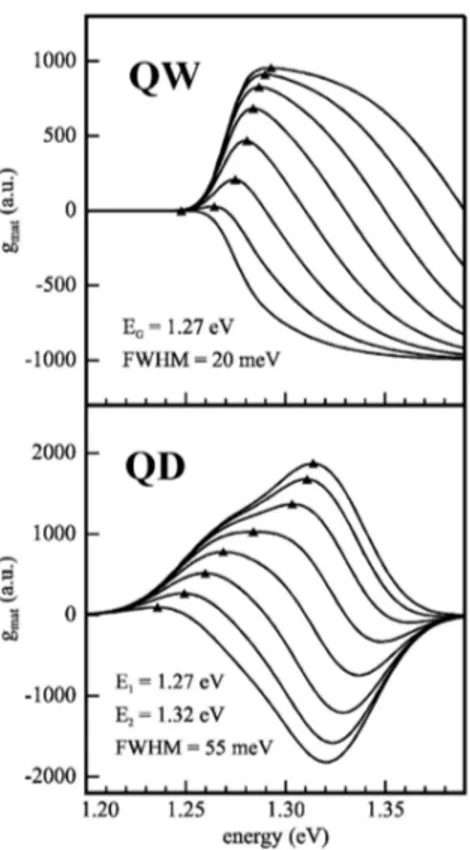
Figure 2-13. Calculated material gain for different quasi-Fermi levels in case of a QW and QD active layer ... 58
Figure 2-14. Potential and particle wave function in the envelope function approximation ... 59
Figure 3-1. Type-II phase matching in the DOPO waveguides at degeneracy ... 66
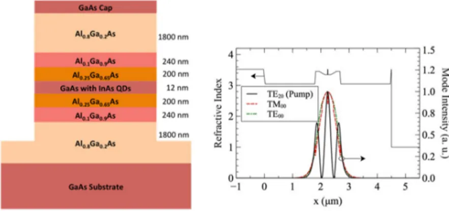
Figure 3-2. Left: epitaxial structure of the GaAs-based diode ... 67
Figure 3-3. Epitaxial structure and interacting modes of the InP-based diode ... 68
Figure 3-4. Index mismatch as a function of ridge width and pump wavelength in the GaAs-based diode ... 68
Figure 3-5. Index mismatch as a function of ridge width and pump wavelength in the InP-based diode ... 69
Figure 3-6. Tunability out of degeneracy of the GaAs-based diode. ... 70
Figure 3-7. Tunability out of degeneracy of the InP-based diode ... 70
Figure 3-8. First symmetric modes supported by the waveguides in the GaAs and InP-based diodes for different numbers of quantum wells ... 73
Figure 3-9. Confinement factors for TE0 and TE2 in multi QW DOPOs and their ratio, as a function of the number of QWs ... 73
Figure 3-10. Variation of the normalized conversion efficiency with ridge width for the GaAs-based diode ... 75
Figure 3-11. Variation of the normalized conversion efficiency with ridge width for the InP-based diode ... 76
Figure 3-12. OPO threshold as a function of signal/idler propagation losses, for several values of normalized conversion efficiency, resonator length and reflectivity
... 77
Figure 3-13 Bandgap and three doping profiles of the GaAs-based structure ... 78
Figure 3-14. Voltage-current curves corresponding to the different doping profiles presented in figure 3-13. ... 78
Figure 3-15. Doping profiles in the InP structure ... 80
Figure 3-16. Voltage-current curve corresponding to the different doping profiles presented in figure 3-15 ... 80
Figure 3-17. Modal gains required to reach the lasing threshold for the GaAs-based and InP-based QW diodes ... 82
Figure 3-18. Material gains required to reach the lasing threshold for the GaAs-based and InP-GaAs-based QW diodes ... 82
Figure 3-19. Threshold current densities for the GaAs-based and InP-based QW diodes. ... 83
Figure 3-20. Threshold current density for a single layer of quantum dots for the GaAs-based QD diode. ... 84
Figure 4-1. Optical setup used for lasers characterization ... 87
Figure 4-2. Surface series resistance as a function of laser length ... 88
Figure 4-3. Threshold current density as a function of laser length ... 89
Figure 4-4. Light-current curve of laser chip n° 1402 against a liner fit above threshold... 89
Figure 4-5. Optical spectrum of laser chip n° 1402 below and above threshold. ... 91
Figure 4-6. Predicted far field intensity for modes TE00 and TE20 (fundamental and first even mode in the direction of growth) vs. angle along the fast axis. ... 91
Figure 4-7. Far field of different lasers. ... 92
Figure 4-8. Far field patterns at different currents for two lasers of different lengths ... 93
Figure 4-9. Far field on the fast axis for a 4 mm laser ... 93
Figure 4-10. Inverse of differential efficiency as a function of length ... 94
Figure 4-11. Comparison between far field and optical spectrum in a 1 mm laser ... 95
Figure 4-12. Required material gain at threshold with and without carrier accumulation between cladding and camelback. ... 96
Figure 5-1. Coupling condition ... 101
Figure 5-2. Difference to the formula proposed by [139], for the relation between Ga and As fraction in InGaAsP lattice-matched to InP ... 102
Figure 5-3. Optical setup for index measurement. ... 105
Figure 5-5. Example of coupling measurement at a wavelength of 1.55 µm ... 108
Figure 5-6. Determination of the refractive index and thickness for a slab of In0.67Ga0.33As0.72P0.28 at λ = 1.55 µm ... 109
Figure 5-7. Determination of the refractive index and core thickness for a slab of In0.67Ga0.33As0.72P0.28 on InP at a wavelength of 1.55 µm ... 109
Figure 5-8. Refractive index measured at 1.55, 2.12 and 3.1 µm vs. y. ... 110
Figure 5-9. Refractive index of InGaAsP lattice-matched to InP vs. wavelength. ... 112
Figure 6-1. General overview of ridge lasers fabrication ... 115
Figure 6-2. General view of the processes used to define AlGaAs structures ... 118
Figure 6-3. Masks used for AlGaAs dry etching and resulting structures ... 122
Figure 6-4. SiN dry etching ... 122
Figure 6-5. Metal mask undulation ... 123
Figure 6-6. RIE and ICP-RIE chambers ... 123
Figure 6-7. Main processes involved in RIE etching. ... 124
Figure 6-8. Examples of large (>1 µm) structures etched by ICP-RIE. ... 126
Figure 6-9. Results of ICP-RIE etching of GaAs with the parameters given in Table 6-1 ... 126
Figure 6-10. Example of structures etched by ICP-RIE. ... 126
Figure 6-11. Etch in typical conditions with and without helium leak in the chamber. ... 128
Figure 6-12. Result of a single ICP etching on pillars of various sizes ... 128
Figure 6-13. Result of ICP etches in typical conditions at different temperatures ... 130
Figure 6-14. Early example of ICP etch. ... 130
Figure 6-15. View of a cleaved waveguide facet before mask removal ... 130
Figure 7-1. Example of evanescent coupling ... 135
Figure 7-2. Bragg-exchange coupler ... 135
Figure 7-3. Adiabatic coupler... 136
Figure 7-4. Resonant coupling ... 137
Figure 7-5. Eigenmodes in an adiabatic coupler. Index mismatch varies continuously from left to right ... 138
Figure 7-6. Transfer in a resonant coupler. ... 139
Figure 7-7. General view of the proposed coupled-cavity design. ... 142
Figure 7-8. Effective indices of guided modes in the structure ... 143
Figure 7-9. SPDC efficiency vs. ridge width in a 0.95 µm thick waveguide surrounded by Al0.8Ga0.2As and air. ... 143
Figure 7-10. OPO pump power threshold for a ridge width of 4 µm and 2 µm as a function of length and signal/idler reflectivity. ... 144
Figure 7-11. Normalized SPDC efficiency as a function of ridge width and thickness.
... 144
Figure 7-12. Normalized SPDC efficiency as a function of ridge width and thickness, for a waveguide temperature of 20°C and 50°C ... 145
Figure 7-13. Normalized SPDC efficiency as a function of ridge width and thickness, for pump wavelengths of 990 nm and 1010 nm. ... 145
Figure 7-14. Tunability curves of the waveguide supporting frequency conversion. ... 147
Figure 7-15. Transverse view of the structure. ... 148
Figure 7-16. BPM simulation of light propagation in the structure and normalized guided power along z, in the upper and lower waveguides ... 148
Figure 7-17. Modal decomposition of the BPM-simulated field in figure 7-16 on the eigenmodes of the GaAs waveguide. ... 149
Figure 7-18. Side and top view of the proposed taper geometry ... 150
Figure 7-19. Power transmitted to the eigenmodes in figure 7-20 ... 151
Figure 7-20. Four eigenmodes of the ridge GaAs waveguide of width 2 µm ... 151
Figure 7-21. Model used to estimate the laser temperature rise ... 152
Figure 7-22. Junction temperature as a function substrate thickness, for three laser lengths. ... 153
List of tables
Table 1. Characteristics of the materials used for three-wave mixing in this thesis
(GaAs and InP) compared to LiNbO3 ... 7
Table 3-1. Modal reflectivities of the first even modes in the structures presented earlier ... 71
Table 3-2. Sources of variations in the effective index mismatch for the structures presented earlier ... 74
Table 3-3. FCA-induced losses for the first two even modes of the waveguide at λp and the fundamental TE mode at 2x λp in the GaAs-based diode. ... 79
Table 3-4. FCA-induced losses for the first two even modes of the waveguide at λp and the fundamental TE mode at 2x λp in the InP-based diode ... 80
Table 3-5. Losses due to FCA in a single quantum well for the structures presented above. ... 84
Table 4-1. Summary of laser characteristics ... 90
Table 5-1. Physical properties and measured indices of the studied samples ... 111
Table 5-2. Parameters of the one-oscillator fit inferred from the index measurements. ... 113
Table 6-1. Typical parameters used for ICP-RIE etches of AlGaAs. ... 125
Table 6-2. Typical parameters used for ICP-RIE etches of SiN. ... 126
Table 7-1. Data sheet of a typical AlGaAs laser ... 134
Table 7-2. Compatibility of different coupler types with the DOPO project ... 136
Table 7-3. Advantages and drawbacks of different coupling geometries. ... 141
Table 7-4. Layer structure proposed for the coupled-cavity design. ... 142
Table 7-5. Coupling constants for fundamental TE and TM modes at 2 µm, given a rectangular grating of depth 200 nm and duty cycle 50%. ... 146
List of acronyms
AR Active Region
BPM Beam Propagation Method
DFG Difference-Frequency Generation
DP-DROPO Double-pass Doubly Resonant Oscillator
DROPO Doubly Resonant Oscillator
DWELL Dot in a well
FCA Free Carrier Absorption
FSMB Fixed Stage Moving Beam
FWHM Full Width at Half Maximum
ICL Interband Cascade Laser
ICP-RIE Inductively Coupled Plasma - Reactive Ion Etching
LI Light-Intensity
NL Nonlinear
OP Orientation Patterned
OPA Optical Parametric Amplification
OPO Optical Parametric Oscillator
MBE Molecular Beam Epitaxy
NIR Near Infrared
PPLN Periodically Poled Lithium Niobate
QD Quantum Dot
QCL Quantum Cascade Laser
QW Quantum Well
RK Runge-Kutta
SFG Sum-Frequency Generation
SHG Second Harmonic Generation
SK Stranski-Krastanov
SPDC Spontaneous Parametric Down-Conversion
SROPO Singly Resonant Optical Parametric Oscillator
TIR Total Internal Reflection
Introduction
Photonics can be described as a field of research started by the invention of the laser [1] and expanded by a transfer of technology from microelectronics. While it spans all aspects of light manipulation, the term “photonics” usually designates it as a cousin of electronics, manipulating photons like electronics manipulates electrons. Two years only after the first operation of a laser, stimulated emission was demonstrated in GaAs diode lasers [2,3]. Since then, new applications appeared at the junction between the two fields. Miniaturization of the components starting with the laser allowed new products to reach the general public thanks to mass fabrication and compactness. Today the field of photonics covers a large number of applications ranging from optical telecommunications, data storage and possibly optical computing in the future to health, defense and security.
Many building blocks of photonic circuits have been demonstrated on silicon, but its lack of a direct band gap has hindered the demonstration of a laser in this material. While Si lasers based on engineered Si-based materials or Raman transitions have been demonstrated [4], the effective usefulness of these techniques is still hampered by low efficiency or lack of electrical pumping. Meanwhile, a large technology developed around III/V laser diodes. After their first demonstration in GaAs, they were based on AlGaAs ternary alloys because of their quasi-null lattice mismatch over their composition range. Then other families were added, like InGaAsP, GaInSb, AlGaInP, InGaN, and now II-VI materials. Threshold currents have been reduced by several orders of magnitude with the introduction of confined heterostructures and progress in epitaxial growth. To date, laser diode technology is best developed in GaAs and InP platforms, and present research in these fields concentrates on the addition of new functionalities.
In the absence of efficient Si-based lasers, silicon photonics relies on the integration of external III/V emitters. To date, two techniques are commonly used for III/V on Si integration. In heterogeneous integration, building blocks from different materials are connected: this method requires delicate coupling and alignment. The other method, which relies on bonding wafers with a polymer, has led to the demonstration of efficient III/V-Si hybrid lasers but does not scale well in mass production. Epitaxy of III-V materials directly on Si is considered a promising solution for large-scale fabrication [5], although it is still at the development stage (the field is going through a renewal after an initial interest in the 90’s [6]).
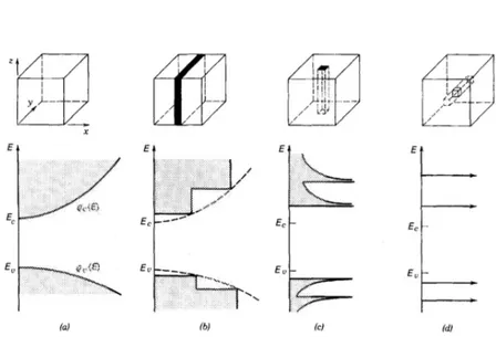
Nowadays, with the progress of the last years on new materials, the total spectrum covered by laser diodes has expanded from the near infrared (NIR) to the entire 400-3300 nm range. However, the emission wavelength of laser diodes is fundamentally set by the material interband transition energy and the constraint of using electronic transitions sets a limit on accessible wavelengths. Making green, orange or ultraviolet laser diodes is still challenging and blue LEDs became available only recently [7]. By exploiting other optical transitions, the spectrum accessible to laser sources has been broadly extended. The first non-diode semiconductor laser was the quantum cascade laser (QCL), proposed in 1971 [8] (figure 1.b). Its core principle is to engineer a superlattice of quantum wells (QWs) so that an electron can cascade down between intersubband levels. The first QCL was demonstrated in 1994 [9], after the development of molecular beam epitaxy (MBE) made it possible to grow semiconductor layers with a precision down to the atomic scale. The possibility of engineering the material transition levels makes QCLs very versatile sources, covering the 3 µm to 300 µm range to this day1. Interband cascade lasers (ICL) are based on a similar concept: electrons cascade down a superlattice but undergo interband transitions (figure 1.c) in the 2-4 µm range. This scheme was proposed in 1995 [11] and demonstrated quickly after [12], but continuous wave (CW) room temperature operation was obtained only in 2008 [13].
To this day, these different sources cover the electromagnetic spectrum from the visible to the far-infrared range. However ICLs, which cover the gap between laser diodes and QCL, are still at an earlier stage of development. Yet the wavelength range from 2 to 4 µm is of particular interest in the spectroscopy community as it contains various rotational and vibrational peaks of atmospheric and hydrocarbon molecules. While resonances of spectroscopic peaks can be measured in the visible / NIR range, their absorption lines are orders of magnitude smaller than in the 2-4 µm range. Monitoring hydrocarbon species with high sensitivity would allow for more
1 With the exception of the Restrahlen band, from 28 to 30 µm. QCLs emitting at longer wavelengths are still limited to the cryogenic regime [10].
Figure 1. Simplified diagram of the band structure of a laser diode, a QCL and an ICL. In the former, carriers recombine between conduction and valence band levels and a limited number of active regions exist. In QCLs, periodic structures are built in which injected electrons undergo transitions between intersubband levels of QWs. After a radiative transition, carriers are injected into another period (injection region are indicated by dashed
lines). ICLs operate with a similar principle, but carriers undergo interband transitions. Figures taken from [14,15].
efficient production, transportation and combustion systems [16]. Methane and carbon dioxide detectors, particularly, are currently sparking interest for environmental monitoring and detection of gas leaks [17]. Other areas of applications include defense and security, with spectral signatures of explosives and biochemical agents or their byproducts around 2 µm [16], and the medical field, with the possibility of portable sensors of atmospheric gases to base diagnosis on breath analysis [18].
Presently, this wavelength range is only partly covered by laser sources. Material constraints limit QCL emission to relatively long wavelengths. Indeed, while emission at 3.4 µm was demonstrated as early as 1998 [19], development to shorter wavelengths has been slow: the limit was pushed to 3.1 µm in 2006 [20], then 2.75 µm one year later [21]. However these sources are limited to a research environment and maximal operation of ≈10°C. The lowest wavelength achieved by a QCL to our knowledge is 2.65 µm [22] at cryogenic temperatures (200K). At room T and in continuous wave (CW), the current limit is still above 3 µm [23]. Bridging the gap from the shorter wavelength side, GaSb diodes have demonstrated emission in the 2-3 µm range [24] and have been used for gas sensing in research environments [25], but at the moment they are not commercially available. ICLs, on the other hand, are
available to the general public - albeit at a high price. Several groups have demonstrated spectroscopic detectors based on ICLs around 3 µm [26,27].
In addition to emission in a particular wavelength range, sources used for spectroscopy should be tunable. This can be induced by changing the peak gain wavelength or cavity resonance. In a standard integrated laser, wavelength is tuned by control of current and temperature, namely through thermo-refractive effect to shift cavity resonance, and through temperature dependence of the gap. Both settings affect the emitted power so that wavelength is not tunable independently of power output. Tunability with these means is limited to a few tens of nanometers and as a consequence, laser diode emitters are usually optimized for the detection of a single chemical species. Several solutions have been developed to produce more widely tunable sources, in order to expand the range of tracked species and increase measurement precision.
A way to do this is via an array of distributed feedback (DFB) lasers providing a wide overall frequency covering by overlapping single lasers ranges [28]. This technique, proposed by [29], is cheaper than fabricating and aligning individual laser diodes because all DFB gratings can be defined on the same wafer. Although a very good wafer homogeneity is required, this technique is well established commercially: companies like Daylight solutions or Pendar Technologies offer broad-spectrum sources based on this principle. QCLs are particularly powerful in that respect because their gain spectrum can be engineered to be as large as desired. A source based on this concept, called heterogeneous QCL, demonstrated tunability from 5 to 10 µm [30]. However, while QCL arrays may be demonstrated in the short-wavelength range in the future, at the moment they operate mostly in the mid-infrared (MIR) range, where QCLs are better controlled.
External cavities also provide large tuning ranges when combined with wide gain sources. QCLs in external cavities are well developed, including for gas monitoring [31]. There has been a lot of effort to propose field-deployable sources, and [32] is an example of miniaturized hand-held external cavity setup. ICLs have also been integrated in external cavities, but they are more upstream to this day: for example [33] shows a tunability of 150 nm around 3.2 µm, albeit with an emitted power of only 4 mW.
In this context, nonlinear optics offers a solution for widely tunable sources from NIR to MIR. One of the effects arising from nonlinear susceptibility of a material is frequency conversion via three-wave mixing. In this case, differently from the
sources presented earlier, the involved energy levels are virtual: the constraint linked to using electronic transitions of the material disappears. All energy levels inside the gap are theoretically accessible and tunability is considerable. A common example of frequency conversion is provided by green lasers, which rely on the second-harmonic generation (SHG) from Nd:YAG or Nd:YVO4 lasers at 1064 nm. Three-wave mixing has also been used to access the 2 - 4 µm region from the MIR emission of QCLs. In that case the nonlinear susceptibility is designed and resonant. The first demonstration of SHG in a QCL was in the 3.6 - 4.7 µm range [34], and SHG at 3.75 µm has also been demonstrated [35].
When a nonlinear medium is placed inside a cavity, a threshold may occur when its parametric gain exceeds losses, similarly to a laser threshold. This system is called an optical parametric oscillator (OPO). Like lasers, OPOs offer a coherent and monochromatic output, and moreover they are continuously tunable over hundreds of nanometers. Many macroscopic OPOs have been developed specifically for spectroscopic sensing in the NIR or MIR [36,37], and some companies offer in situ diagnostics based on these tools (e.g. Blue Industry and Science, Quantel Lasers). However, they are more delicate to control than lasers. This is mostly due to the phase-matching condition: waves at different frequencies must stay in phase, which sets a constraint on their refractive indices. For example, in the case of SHG, indices of fundamental and harmonic must be equal. This being generally impossible because of chromatic dispersion, birefringence is often used for frequency conversion. The phase-matching condition limits the types of suitable materials and makes OPOs very sensitive to environmental variations. To date, OPOs mostly remain bulky lab-based systems, operated by specialists of nonlinear optics.
Historically, the standard gain material of nonlinear optics is LiNbO3, used for its birefringence, wide transparency range and high nonlinear quality factor2. The first OPO was demonstrated with a birefringent LiNbO3 crystal [38]. In 1993, periodically poled LiNbO3 (PPLN) was fabricated by the application of an intense electric field on the material at the micrometric scale [39], enabling a novel phase-matching technique, called quasi-phase matching (QPM) [40]. Instead of controlling the
2 The quality factor for three-wave mixing is (2)/n3 where (2) is the second-order
effective indices to satisfy phase relations, the fields are left free to go out of phase and the sign of (2) is periodically reversed to compensate for this. Other periodically poled materials have been demonstrated, like ppKT, ppLiTaO3, ppRTA… To date these crystals remain the most widely used in visible and NIR OPOs.
In parallel with the use of bulk crystals, there has been an effort to exploit frequency conversion in waveguides because they provide higher field intensities and interaction lengths. Despite the drawbacks of using waveguides, which are for the moment higher propagation losses and complex fabrication, today there is already a large range of integrated optical components in LiNbO3, including PPLN waveguides for frequency conversion [41].
More recently, semiconductors have also been used for frequency conversion, enabling the integration of light generation, conversion, processing and detection on the same chip. These materials often have remarkable nonlinear properties compared to ferroelectric crystals (see table 1).
While there is a large field of research on nonlinear processes in silicon, this crystal does not have second-order susceptibility (see chapter 1 for the definition of higher-order susceptibilities) because it presents inversion symmetry. As a consequence, three-wave mixing processes cannot occur in it unless strain is induced. Frequency conversion and OPOs based on four-wave mixing in Si have been demonstrated, but the frequencies involved in these processes are in the same range. Thus these sources cannot provide access to a different part of the optical spectrum as in the case of three-wave mixing.
On the other hand, III/V compounds have a second-order susceptibility. To date, most of nonlinear optics in III/Vs occurs in GaAs because of its high quality factor and mature technology.
GaAs was not commonly used in frequency conversion before the 1990’s because it lacks birefringence, like all cubic crystals. Several techniques (which we will revisit in chapter 1) have been developed to satisfy phase matching in this material.
Historically, the first phase-matching technique makes use of orientation-patterned GaAs (OP-GaAs). Nonlinear optics based on GaAs expanded dramatically after the first fabrication of this material [43], which quickly led to the demonstration of an OPO [44]. Today OP-GaAs in macroscopic cavities shows performances comparable to traditional media, with e.g. CW output power over 3 W, 45 % efficiency and M²=1.5 [45,46]. To date, losses at short wavelength and a complex fabrication
technology hinder the exploitation of OP-GaAs waveguides in the NIR, while a MIR OPO based on a OP-GaAs waveguide was demonstrated in 2012 [47]. At present propagation losses and the lack of GaAs-based source at 2 µm remain the main limitation of this platform. For this reason, OP-GaSb is being developed to integrate source and QPM conversion in the same material [48], and upstream material studies for orientation-patterning in other III/Vs are starting to emerge [49,50].
Material Refractive index n (at λ = 1 µm) 2nd-order susceptibility deff [pm/V] (at λ = 1 µm) Figure of merit deff²/n3 [pm/V] Thermal conductivity [W/m.K] LiNbO3 2.23 25 59 5.6 GaAs 3.5 170 674 45 InP 3.29 1304 474 68
Table 1. Characteristics of the materials used for three-wave mixing in this thesis (GaAs and InP) compared to LiNbO3. deff is the most used nonlinear coefficient. Note that in AlGaAs
and InGaAsP, alloy scattering decreases the thermal conductivity down to 1 order of magnitude.
Another technique to make GaAs exploitable for guided-wave nonlinear optics is based on form birefringence through the insertion of thin layers of different index, as proposed in [51]. This scheme originally relied on layers of different Al content in AlGaAs, but was limited by the low index contrast. Oxidation of layers with high Al content [52] permitted the demonstration of an OPO threshold in a micrometric waveguide [53]. To further increase index contrast, it was proposed to use selective etching in order to create a structure pierced by thin layers of air [54]. To date, the main limit of the AlOx-based technique is set by the losses induced by impurities leftover from the oxidation process. More fundamentally, this scheme cannot be easily integrated with electrical injection since AlOx layers are insulating. Furthermore, symmetry conditions of GaAs limit use of this technique to TM-polarized pumps. This is a strong limitation since common semiconductor sources in the near-infrared are QW laser diodes, with TE polarized emission.
3 Manufacturer value.
Both the above methods are based on complex material patterning that introduces propagation losses and other intrinsic limitations. Fortunately, a third phase-matching strategy exists, which is relatively easy to implement and does not require significant deviations from traditional laser and waveguide design: modal phase matching. This technique simply relies on the engineering of modal dispersion in a waveguide to compensate for material dispersion. Among the possible schemes, a significant one is the use of Bragg and total-internal reflection (TIR) modes, introduced in [55]. This design has led to the demonstration of a twin-photon source [56] and a twin-photon laser diode [57]. Intracavity conversion in a laser diode [58] has also been achieved, as well as a widely tunable source around 2 µm [59]. However, no OPO based on modal phase matching has been demonstrated to date, regardless of several design proposals [60,61].
Despite five decades of progress after the invention of the first OPO, no electrically injected OPO on-chip has been demonstrated, although OPO threshold was reached in optically pumped waveguides [47,53] and intracavity conversion was obtained in a laser diode [58].
In this context, this thesis presents the work towards optical parametric oscillation inside a laser diode. We describe the design of two sources, based on GaAs (InP) for emission at 1 µm (1.55 µm) and down-conversion around 2 µm (3 µm). These emitters would provide widely tunable sources in the 2-4 µm range.
The design presented in this thesis is based on modal phase matching, since this technique is compatible with electrical injection and TE-polarized sources in the NIR. Ridge width is used as a degree of freedom to control phase mismatch after epitaxy in narrow, deeply etched waveguides. As a consequence, quantum dots (QDs) and dashes are proposed as active area medium in order to limit non-radiative recombination on the sidewalls [62].
The development of these sources is a joint project of Paris Diderot University, CEA Grenoble and the III-V Lab. Advances made during this thesis were shared between these labs and my PhD was split between Paris Diderot and CEA Grenoble. The original idea of diode-OPO, based on GaAs, is presented in [61]. The III-V Lab fabricated broad-area QW lasers based on this design and I characterized them. In parallel, I started establishing a fabrication process of narrow deeply-etched laser diodes. In addition, to transfer the concept to the InP platform, I built an m-lines setup and measured the refractive index of InGaAsP at 3 µm. Then, on the base of these measurements, I designed an InP-based phase-matched diode. Finally, I
conceived an alternative design for light generation and conversion in two distinct albeit monolithic cavities linked by a vertical coupler.
This work is organized as follows. Chapters 1 and 2are an introduction to the physics of the systems used in this thesis. Nonlinear optics in waveguides is presented in chapter 1 and QD / QW laser diodes in chapter 2. I focus particularly on doubly and triply resonant OPO thresholds, and on the impact of propagation losses for frequency conversion. Concerning laser diodes, this text is a general introduction but it shows the specificities of QW vs. QD diodes. Chapter 3 presents the diode-OPO concept and the two designs based on this idea in the GaAs and InP platforms. In chapter 4, I report on my characterizations of broad area QW laser diodes based on the GaAs vertical structure. Chapter 5 shows the refractive index measurements of InGaAsP in the NIR-MIR range, on which I established the design of chapter 2. Chapter 6 is devoted to fabrication efforts undertaken to develop narrow, deeply-etched laser diodes. Finally, in chapter 7 I provide an alternative design based on a vertical coupler.
1. Three-wave mixing in GaAs
We give here an overview of three waves mixing processes in waveguides. Optical parametric amplification (OPA) and oscillation (OPO) are described in the cases of null or finite propagation losses. We extend our description to the case of a triply resonant oscillator (TROPO) and discuss phase-matching strategies in GaAs.
Nonlinear optics in plane waves
From the nonlinear polarization to the coupled equations
Frequency mixing and other nonlinear effects arise from the electronic response of a material under intense electric field. The basic description of polarization in a dielectric is
where 𝜀 is the vacuum permittivity and 𝜒 is the dielectric susceptibility of the material.
Under limited electric field, this picture is sufficient. However, shortly after the first demonstration of lasers [1], their intense electric fields allowed for the demonstration of higher-order effects in the polarization [63]. In this description, for a homogeneous and time-invariant dielectric material, having a local response in time and space, the polarization is expressed as
where 𝜒( ) is the i-th order susceptibility of the material, that is a tensor of rank i+1:
𝜒( ) is a 3x3 matrix, 𝜒( )a 3x3x3 tensor, etc. The first term of this equation corresponds to the linear response of the polarization, while the sum of other terms is commonly called “nonlinear polarization” or PNL. The susceptibility amplitudes decrease very fast with their order, which is why they can only be revealed at high electric fields. The various components of the nonlinear susceptibility result in different effects. In particular, 𝜒( ) gives rise to three-wave mixing, 𝜒( ) to
four-wave mixing, and so forth. Since this thesis concentrates on 𝜒( )effects, we will
Polarization in return feeds back the electric field. In a non-magnetic, isotropic and dielectric optical medium with no free charges or currents, the following wave equation stands [64]:
In other words, the nonlinear terms of the polarization act as source terms for the electric field.
To solve for 𝐸⃗ in (1.3), it is usual to write the electric field as a superposition of plane waves in Fourier domain:
where c.c. stands for complex conjugate.
Similarly, the second-order polarization can be developed in Fourier domain, by injecting (1.4) into (1.2). For energy conservation, each (angular) frequency is determined by the other two, which is why the argument of the polarization is often written as (-ω1; ω2, ω3). Then, if the frequencies satisfy ωl = ωm + ωn, the component of P(2) along the i-th axis is:
The nonlinear susceptibility can be simplified thanks to symmetry of the material. For example, in centrosymmetric crystals like Si, susceptibility tensors of even rank vanish. Far from the material resonances, where dispersion is negligible, Kleinman symmetry applies. As a consequence, the tensor 𝜒( ) can be written in a
contracted form 𝑑 = (1/2) 𝜒( ) . The l index corresponds to (j, k) pairs and ranges from only 1 to 6 thanks to symmetries of the material reducing the number of independent components. (The factor ½ is present for historical reasons). In GaAs, the only non-vanishing element of 𝑑 is 𝑑 , equal to ≈120 pm/V in the NIR.
We will now consider an electric field made of three monochromatic plane waves at ω1, ω2 and ω3 = ω1 + ω2.Injecting (1.4) and (1.5) into (1.3) with the slowly-varying-envelope approximation yields the following coupled equations:
where ∆𝑘, defined as k3 – k1 – k2, is called the phase mismatch; ni is the refractive index at ωi; deff an effective nonlinear susceptibility (determined by waves polarizations and crystal symmetries); and D a degeneracy factor equal to 2 if the wave at ω1 and ω2 are distinguishable, and 1 otherwise.
These are the fundamental equations describing frequency mixing in nonlinear optical media. From there we can make the following remarks. Firstly, unless phase mismatch is null, the oscillating term 𝑒 prevents consistent build-up or depletion of the fields. Control of the phase mismatch is thus critical to frequency mixing. This can also be interpreted as a conservation of the total photon momentum: k3 = k1 + k2. Secondly, the coupled equations of nonlinear optics yield fundamental conservation relations. In a quantum description, the photon flux at ωi is given by Ii / (ħωi) where Ii is the intensity. The quantities Ii/ωi are then proportional to the flux of photons per unit time per unit area for the frequency ωi and the coupled equations can also be expressed as
These conservation relations are known as Manley-Rowe relations. They convey the conservation of energy during the frequency mixing process in a quantum description: for each photon destroyed at ω3, one has to appear at ω2 and one at ω1.
Three-wave mixing processes
Figure 1-1 shows the processes allowed by three-wave mixing.
In sum-frequency generation (SFG), two waves at frequencies ω1 and ω2 combine to create a wave at the sum frequency ω3. Second-harmonic generation (SHG) is a degenerate case of this process. In this case, a wave interacts with itself to create a field at the frequency ω3 = 2 ω1.
In difference-frequency generation (DFG)or optical parametric amplification (OPA), a field at ω3 (usually called the pump field) interacts with a field present at the crystal entrance (the seed), of frequency ω2, to generate a wave at ω1. Manley-Rowe relations
still apply, so the seed is amplified as well. The generated field of higher frequency and its complementary are usually called signaland idler, respectively.
Parametric fluorescenceis similar to OPA, with the difference that no seed is present at the crystal input. This process is quantum in nature: an analogy can be made with the classical description of stimulated emission in lasers vs. quantum description of spontaneous emission.
The work presented in this thesis aims at an optical parametric oscillator. In this system, the nonlinear medium is placed inside a cavity resonating either at frequency ω1 (singly-resonant OPO), ω1 and ω2 (doubly-resonant OPO) or ω1, ω2 and ω3 (triply-resonant OPO). When nonlinear gain exceeds losses, a threshold appears in the converted light power, similarly to the case of a laser threshold: it is said that the system oscillates. While OPA can only be jump-started by parametric fluorescence, in a stable regime a constant signal / idler field exists and provides a seed for the three-wave mixing. These systems are described by the equations of OPA completed by self-consistent conditions after a cavity round-trip.
Figure 1-1. Three-wave mixing interactions. Left: waves amplitudes in a nonlinear medium. Right: virtual transitions, solid (dashed) lines corresponding to real (virtual) energy levels.
Second-harmonic generation
We will examine here the simple case of second harmonic generation to illustrate fundamental concepts of three-wave mixing. In the case of SHG, (1.6) reduces to
A common approximation is to assume non-depletion of the pump: the efficiency of frequency conversion is small enough for the pump power loss to be negligible. In this thesis, such assumption is largely justified and it will be made unless otherwise specified. E2ω can then be set constant in (1.8), from which we deduce Eω(z). The generated wave power is given by P2ω = A I = A (½ ε0 c n |E2ω²|) where A is the field area. P2ω turns out to be proportional to the square of Pω, which allows us to define the conversion efficiency ηSHG and normalized conversion efficiency η0norm as [64]
Since the normalized conversion efficiency does not depend on L, it is a convenient figure to compare SHG in different crystals.
From this simple description, we can observe the following features, which also hold for other types of processes:
- Generated power grows quadratically with distance and nonlinearity at phase matching.
- If the phase mismatch is not null, we can define the coherence length Lc = π/Δk. The generated field builds up during a length Lc, then decreases between Lc and 2Lc. This variation is periodic, with the amplitude and period of energy exchange depending on Lc, and it arises from the interference between the generated and pump fields: if Δk≠0, the generated wave becomes more and more dephased with respect to the pump as it propagates, until it is shifted at Lc, where the direction of energy transfer is inverted. This is shown in figure 1-2 for several values of Lc.
- At fixed length, if k≠0, the conversion efficiency is affected by a rapidly decreasing function of ΔkL. This is represented in figure 1-3.
Figure 1-2. SHG conversion efficiency for different values of coherence length. Solid blue line: Lc = ∞ (Δk = 0), dashed yellow line: Lc = 3, red dot-dashed line: Lc = 1.
Figure 1-3. Normalized SHG conversion efficiency vs. normalized phase mismatch.
Optical parametric amplification
In the case of OPA, we make once more the undepleted-pump assumption. Then E3 is constant in (1.6) and its solution becomes [64]
We will call g the gain coefficient and Ps,i/Ps,i(0) the gain G. Note that the gain coefficient g0 is higher at degeneracy and that in this case we can write g = (η0norm Pp)1/2, where η0norm is the normalized conversion efficiency of SHG. In the long range, still in the undepleted pump approximation, the gain is exponential in the case of phase-matching. In the case where signal and idler are indiscernible and of same amplitude at z = 0, still assuming phase-matching, G = (cosh²(gz)+sinh²(gz)). Taking
the weak gain approximation gL<<1 (verified in this thesis), the gain in this particular case takes the form G ∼ (1+2g²z²).
Nonlinear optics in waveguides
Effective area
Hereafter, we will consider eigenmodes propagating in waveguides. The electric field of the mth eigenmode in a waveguide is given by
where ϕm [m-1] is the spatial distribution of the electric field in the transverse plane, ε [V] is the slowly varying part of the electric field in the direction of propagation, 𝑒⃗ is the direction of polarization and βm is the propagation constant. The wave equation (1.3) can be solved similarly to the case of plane waves [65], with a few substitutions in the results. Material indices are replaced by modal effective indices. Wave vectors ki are replaced by propagation constants βi = 2π ni / λ0i, where λ0i is the wavelength in vacuum. The shift from plane waves to eigenmodes of various transverse profiles makes necessary the use of the nonlinear overlap integral Γ, defined as
In the case of SHG and OPA presented earlier, the conversion efficiency and the gain coefficient become:
For SHG:
For OPA:
Other definitions stay identical to the plane-wave case.
expresses the overall overlap between the interacting modes and the effective nonlinearity, and its maximization is crucial for the design of efficient nonlinear devices: the effective nonlinearity should be highest where all the three fields are most confined, and nonlinear processes are more efficient between modes of same order.
SHG in the presence of losses
Waveguides offer strong confinement at the wavelength scale, which gives rise to high optical intensities and more efficient nonlinear interactions. However, they can introduce non-negligible optical losses due to surface scattering or absorption, all the more important as the electric field explores the core/cladding interface in a small-section waveguide. Of course they come along with usual absorption, two-photon absorption and free carrier absorption (FCA), which occur also in bulk optics. We will describe SHG and OPA for modes propagating in lossy waveguides. In the presence of linear losses, the coupled equations of SHG become
where αω and α2ω [m-1] are the power loss coefficients at frequencies ω and 2ω, and ε is the slowly varying part of the electric field of (1.12).
We make again the assumption of undepleted pump, which here means that the pump losses due to the nonlinear interaction are negligible compared to other losses. The pump amplitude along propagation is then simply given by an exponential variation:
The solution of (1.16) results in [66]:
Losses have a double impact: they lower the conversion efficiency and relax the phase-matching condition. This is illustrated in figure 1-4, showing the normalized conversion efficiency as a function of phase mismatch for various values of α2ω. As losses increase, the relative weight of the sinc function decreases and the full width at half maximum (FWHM) increases.
Figure 1-5 shows the conversion efficiency as a function of waveguide length for different values of αω and α2ω, in the case of perfect phase matching. When one field experiences losses, the conversion efficiency reaches a limit value and when both fields do, an optimal length appears.
Figure 1-4. Normalized SHG conversion efficiency, L=1 cm-1, for αω = 0 and α2ω = 0, 1, 2, 3
and 4 cm-1 from top to bottom.
Figure 1-5. SHG conversion efficiency as a function of propagation length, for different levels of losses.
OPA in the presence of losses
Let us present the solution for OPA in lossy waveguides in the case of perfect phase-matching only. In the approximation of undepleted pump, the coupled equations become
The solution to this system is given by [67]
where αsi is the value of propagation losses at signal and idler wavelength (they are supposed equal) and G(z) is a gain function depending on the position:
These equations are extremely similar to the case of OPA in a lossless medium (1.10), with a few differences:
- The gain coefficient g0 is modulated by a gain function depending on the position. At fixed position L, g0 decreases by a factor depending on pump losses only.
- The general form of fields amplitudes is similar to (1.10), but is additionally affected by an exponential decrease depending on the signal/idler loss coefficient.
Note that while the authors of [67] claim to work in the low-loss approximation, the only limitation set on losses is that they should be low enough to satisfy the approximation of slowly varying envelope. This is largely verified for the typical loss values in this thesis.
Furthermore, (1.22) and (1.23) are valid solutions of (1.20) and (1.21) regardless of the sign of αp: they hold in the case of pump amplification as well as absorption.
OPA in the presence of gain
We choose to show the effect of pump gain as well as loss because this thesis is focused on the study of a laser-OPO. In this device, laser and OPO cavity are one and the same, and the OPO pump is provided by the laser field. In a laser at threshold, the field experiences a spatial variation that compensates for mirror losses (see figure 1-10):
where we define γ as a “gain” or spatial variation. (Note that it is not the modal gain at threshold, which must equal the sum of mirror and propagation losses). In a laser of 1 mm with uncoated facets, R is typically in the range of 0.33 for the fundamental mode so γ is approximately 11 cm-1. Lasers / OPOs presented here have higher pump reflectivities (R = 0.67), so this effect is less pronounced (γ = 4 cm-1 to 1.3 cm-1 for lasers of 1 to 3 mm).
Figure 1-6 shows the effect of both signal/idler losses and pump gain/losses on the OPA power at degeneracy (ωs = ωi), for parameters in the typical range of the devices presented in this thesis. As expected, signal/idler variation goes from quadratic amplification to exponential decrease as the signal/idler losses increase. Pump gain can compensate for signal/idler losses (dash-dotted red curve), in which case longer waveguides are advantageous, but this effect is small and limited by the weak nonlinear gain set here.
Figure 1-6. OPA gain vs. L, for g0 = 1cm-1 and s=i = 0, 1, 2 cm-1 (blue, red, yellow). Solid
OPOs
When a nonlinear medium is placed inside a cavity, a threshold occurs for the generated field if the nonlinear gain overcomes losses. This is analogous to the laser threshold observed when a gain medium is placed inside a resonant cavity. The ensemble of nonlinear gain medium and cavity is an OPO. Unlike lasers, OPOs do not rely on the transitions between energy eigenlevels of valence electrons in matter. The energy levels involved are virtual, and can be controlled with external settings like temperature or crystal inclination. As a consequence, frequency output is tunable over a large wavelength range. OPOs today provide reliable sources of coherent, monochromatic light with much larger tunability than lasers.
One or several fields may be set in resonance in an OPO. OPOs where either the idler or the signal is reflected is usually called singly-resonant (SROPOs); those where both signal and idler are reflected are called doubly-resonant OPOs (DROPOs), and those where all three fields are resonating, triply-resonant OPOs (TROPOs). (Less common systems include cavities where signal and pump are resonating. For clarity they are usually called pump-signal OPOs instead of DROPOs). Increasing the number of resonating fields lowers the threshold power but degrades spectral stability.
Figure 1-7. Common OPO configurations. Pump, signal and idler are represented in blue, red and green, respectively. Figure taken from [68]
The core of this PhD thesis deals with a laser diode – OPO in which laser and OPO cavities coincide and the laser beam acts a pump field. To lower the oscillation threshold, the design includes high-reflectivity mirrors at both signal and idler wavelengths. Since the pump obviously resonates to provide the laser effect, this device is a triply resonant oscillator. In the last chapter of this thesis, we also present the design of a DROPO that is vertically coupled with a monolithic but distinct laser
diode. Since no SROPOs are present in this thesis, their description is skipped but their characteristics can be inferred by setting Ri = 0 in the equations describing DROPO behavior.
Single pass DROPO
The threshold gain of a DROPO is found by setting the fields equal to themselves after a round trip in (1.22). Undepleted pump is assumed, unless otherwise specified.
Without propagation losses
Without propagation losses, in the case of weak gain, high reflectivity and perfect phase-matching, the gain at threshold is given by [69]
The phase-matched pump threshold is then found by injecting (1.24) into (1.15). An approximate way to include (low) propagation losses in this estimation is to replace Rs,i with Rs,i exp(-αs,iL).
With propagation losses
With propagation losses, the gain coefficient is replaced by a gain function that depends on the position (as we have seen for OPA), and the pump threshold in the phase-matched case becomes [69]:
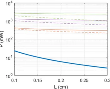
This is valid without approximation on losses, nonlinear gain or reflectivities. The DROPO threshold as a function of resonator length is shown in figure 1-8, for various values of propagation losses. Dashed lines correspond to the small losses approximation (1.24) and solid lines to the general case (1.25).
Using longer cavities has a clear interest in terms of threshold power: in the case of null propagation losses, switching from a 1 mm to 3 mm cavity decreases the pump threshold power by one order of magnitude. At higher loss levels, this effect