HAL Id: hal-00920126
https://hal.archives-ouvertes.fr/hal-00920126
Submitted on 10 Mar 2014
HAL is a multi-disciplinary open access archive for the deposit and dissemination of sci-entific research documents, whether they are pub-lished or not. The documents may come from teaching and research institutions in France or abroad, or from public or private research centers.
L’archive ouverte pluridisciplinaire HAL, est destinée au dépôt et à la diffusion de documents scientifiques de niveau recherche, publiés ou non, émanant des établissements d’enseignement et de recherche français ou étrangers, des laboratoires publics ou privés.
First-principles density functional theory study of
strained wurtzite InP and InAs
Chahira Hajlaoui, Laurent Pedesseau, Faical Raouafi, F. Ben Cheikhlarbi,
Jacky Even, Jean-Marc Jancu
To cite this version:
Chahira Hajlaoui, Laurent Pedesseau, Faical Raouafi, F. Ben Cheikhlarbi, Jacky Even, et al.. First-principles density functional theory study of strained wurtzite InP and InAs. Journal of Physics D: Applied Physics, IOP Publishing, 2013, 46 (50), pp.505106. �10.1088/0022-3727/46/50/505106�. �hal-00920126�
First-principles density functional theory study of
strainedwurtziteInP and InAs
C. Hajlaoui1, 2, L. Pedesseau1, F. Raouafi2, F. Ben CheikhLarbi2, J.Even1,and J.-M. Jancu1*
1
Université Européenne de Bretagne, INSA, FOTON, UMR 6082, 35708 Rennes, France
2
Laboratoire de physico-chimie, des microstructures et des micro-systèmes, Institut Préparatoire aux Études Scientifiques et Techniques, Université de Carthage, BP51, 2070 La Marsa, Tunisie
Abstract.
We report onsemilocal and hybriddensity functional theory (DFT) studyof strainedwurtzitecrystals of InAs and InP. The crystal-field splitting has a large and non-linear dependence on strain for both crystals.Moreover, the study of the electronic deformation potentials reveals that the well-known quasi-cubic (QC) approximation fails to reproduce the non-ideal c/a ratio. This theoretical study is of crucial importance for the simulation of self-assembled InAs/InP nanowires.
Semiconductor core/shellnanowires (NWs)1,2hold lot of promises for applications in the
field in electronics3,4,photonics5,6, and biochemical sensors.7 These systems, compared to pure
semiconductor wires, demonstrate areductionof surface scattering and ionized impurity scattering8with improved electronic confinement properties. The synthesis processis mainly based
on the gold-catalyzed vapor liquid-solid (VLS) growth mechanisms, which allows for a precise controlof geometrical dimensionsand strain accommodation.9The VLS method is particularly suited
in interfacing highly strained III-V materials onto Si substrates.10Interestingly, it favors the
hexagonal phase at the nucleation stage leading toa crystallization of III-V semiconductorsinahexagonal wurtzite (WZ) structure whereasthe bulk counterpart for most of them is cubic zinc-blende (ZB).11Recently, much effort has been devoted to the growth and fabrication of
strained InP/InAs/InPNW devices for the realizationof high field-effect electron mobility transistors and circuits. Advantages of thesesystems include the high electron mobility (30 000 cm2/V s at 300
K) and velocity (43000 cm/s) of InAsand a large conduction band offset between InAs and InP(0.5 eV).12Strain engineering is a well-established technique to tune the electronic band gap of
nanostructures. For instance,the lattice mismatch ofInAs onInPis about -3 %and it is expected to tailor the band offsets and carrier mobility by lifting the degeneracy in the electronic bands. In addition, strain effects cangeneratea piezoelectric polarization charge at interfaces leading to a band bending in the active region of the wire.Determining thematerials properties ofInAs/InP NWs iskey to improving current generating efficiencies of underlying devices.The WZ and ZB band structuresfor bulk InAs and InPhave been extensively studied both theoretically and experimentally.12-14Moreover, electronic deformation potentials (DPs) of cubic semiconductors are
well documented in literature.12However, to the best of our knowledge,no workon DPs has dealt
withWZ III-V materials so far. This first step is mandatory for realistic modeling of InAs/InP NWs in the WZ structure15, including the effects of linear and non-linear electro-elastic coupling.16
In this work , we performab initio calculationsofdeformation potentials in wurtziteInAs and InP. The structural relaxations with strain perturbations are performed using the plane-wave
projector augmented wave method (PAW) as implemented in the VASP code.17 We used the
Heyd-Scuseria-Ernzerhof (HSE06) DFT hybrid exchange correlation functional18,19 with a screening
parameter μ=0.2 and a mixing parameter of α = 0.25. This approach has been foundto give reliable resultsin group III-nitrides20 and group II-oxides.21Generalized-Gradient Approximation (GGA) in
the Perdew–Burke–Ernzerhof (PBE) parameterization22and single shot GW (G0W0) calculations
implemented in VASP are also performed for comparison. We used GGA eigenvalues as input to the single shot G0W0 calculations leading to more reliable parameters such as band gap and
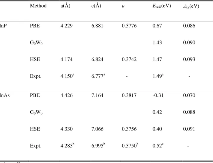
deformation potentials.The semi-core d-electrons of Inaretreated as valence electrons.The procedure is carried out with a plane-wave cutoff of 600 eV and a 6x6x4 Monkhorst–Pack mesh for k-point sampling. This allows for a full relaxationof the structural parameters.The accuracy of the predicted equilibrium lattice constants for both InP and InAscorrelates directly with the level of approximation in the functional as shown in Table I. HSE gives the most accurate resultsandthe well-known overcorrection ofGGA-PBE23become apparent. We also note in Tab. Ithat the
WZstructure is not perfectly tetrahedral with non-ideal c/a and u(an ideal WZ lattice consists ina tetragonal ratio c/a=1.633 of the lattice constants and an ideal internal cell parameter u=3/8)as found for bothsimulations and experiment.
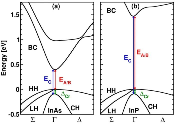
Fig. 1 shows the InAs and InPband structures at equilibrium near the -point computed with HSE. Calculations are performed without spin-orbit coupling. The direct band gap is formed by an s-like 1c(BC)conduction-band state and doubly degenerate p-like 6v(HH, LH) and
1v(CH)valence-band states. Two energy gaps can be defined according to the optical transitions:6v1c (A, B) and 1v1c (C). In our simulations, EA/B is the fundamental transition
energyforboth InAs and InP. As evidenced in Fig. 1, away from the Brillouin zone-center,the valence bands are strongly admixed and their dispersion is non-parabolic.Therefore the valence-band effective massescannot be easily derived for application in k.p models. On the other hand, the conduction band energy dispersionis parabolic near the -point and ourHSEcalculation of the electron masses perpendicular and parallel to the c-axis gives: 0.055 and 0.032 (in units of free
electron mass).These results are consistent with thoseof De and Prior obtained within an empirical pseudopotentialapproach.24As seen in Tab. I, the band-gap energy issensitive to the details of the
exchange and correlation functionaland both the hybrid functionaland single G0W0 reproducevalues
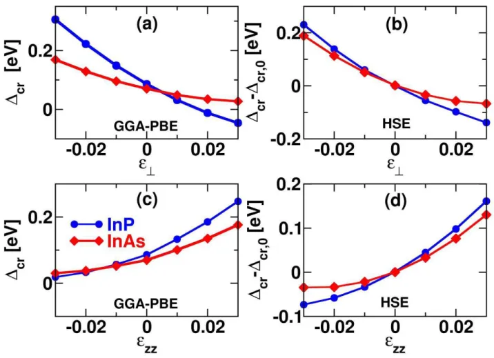
close tothe experimental data.Conversely, an equivalent crystal field splitting cr=HH-CHis obtainedfor PBE and HSEandthe value of InAscompares well with the self-consistent GW calculationof Zanoliet al.12,13A similar behavior between PBE and HSE for cr under deformation is evidenced both for biaxial strain and for uniaxial strain zzas shown in Fig.2. As definition,= (xx+yy)and zzstand for the strain components in and perpendicular of the c-plane. In the calculations, the internal parameter uwas fully relaxed for each strain. Anonlinear behavior is observed for the two semiconductorswhichcan be interpolatedwitha polynomial regression. It should be noted that (Fig. 2b) HSE exhibits a strong nonlinearity for the crystal field splitting of InAs even for moderate biaxial strain.
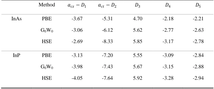
Theelectronic deformation potentials are defined as the linear coefficients in the expansion of the k.p band energies with respect to strain. Weinterpolatedthe present first-principle calculationsfor small deformationswith a derivation ofDPs from a 3x3 band k.p model25which gives
the linear dependence of EA/B and ECon strain as:
/ = / 0 + �� − 1 � + ��� − 2 �⊥ − ( 3� + 4�⊥)
= 0 + �� − 1 � + ��� − 2 �⊥
(acz, act) and (D1, D2, D3, D4) characterize thedeformation potentialsof 1cand1vand
6vrespectively.These relations are compatible with hexagonal symmetry C6v. On the other hand, the breaking of symmetryC6v to orthorhombic C2v with in-plane anisotropic strain lifts the degeneracy ofHH and LH levels as:
� = ��− � = 2 5(� − � )
evidenced between PBE, G0W0, and HSE. However, the calculations ensure an overall uniform
behavior for the DPsincreasingdistinctly from InAs to InP.This trend with the band-gap has beenalso observed in group III-nitrides20 and group II-oxides.21Moreover, the band-gap-related
deformation potentialsofacz-D1and act-D2are found more sensitive to exchange correlation
functionalthan D3, D4 and D5. Because there is currently no available experimental information and
in order to gain insight into the quality of our simulations, we performed DP simulationsin ZB InAs and InP as a test. By comparison to our previous DFT-LDA calculations26,HSE-based calculations
lead to a better agreement with experiment.The same conclusion is drawn from our present GGA computation. This gives us confidence in the ability of the hybrid functional to model deformation potentialsin wurtzite III-V semiconductors.Finally,the QC approximation wastested for InAs and InP from HSE results. The QC approximation is extensively used in k.pHamiltonians and based on a similar local atomic coordination between WZ and ZB crystals leading to a correlation of their physical properties along the [111] direction of the zinc-blende. Herein, we evaluated the deviation from the QC approximation of deformation potentials.Indeed, the same approximation in k.p theorylead to: 3+ 2 4 = 0and 1+ 3 = 2. Actually, neither for InAs nor InPsatisfiedthese
equations.For instance the first one yields-0.93 eV forInP and the failure must be related to the non-ideal c/a ratio.
As a conclusion, a systematic study of the electronic band structure in wurtziteInAsand InP is presented. Hybrid-functional calculations allow for a realistic description of the strained band energies. From accurate calculations of the electronic deformation potentials, we found the widely used QC approximation is not fulfilledfor both InAs and InP. We demonstrated that the dependence of electronic bands on strain is strongly nonlinear and it should be taken into account for a proper modeling of InAs/InP nanowire-based devices.
Figure captions.
Figure 1: Blow-up of the WZ-InAs (a) and WZ-InP (b) band structurescalculated with HSEclose to
the point. anddenote the in-plane and parallel directions with respect toc- axis. The origin of the energy scale is taken at the top of the valence band (VBM).
Figure 2: Left Panel:GGA-PBE dependence of the crystal-field splitting cr()of InAs and InPon (a) in-plane and(c) perpendicular strain with respect to the c-plane. Right Panel: Dependence of
cr()-cr(0) on (b) in-planeand(d) perpendicular straincalculated with HSE for InAs and InP. Quantization axis z is along the[0001] WZ direction.
Tables.
Table I:Results of GGA-PBE, HSE,and G0W0calculations forwurtziteInAs and InP at equilibrium
for the lattice constants (a, c), internal parameter u, direct band gapEA/B, crystal-field splitting cr, and compared with the experimental values2,14,27 (Expt.).Single G0W0 is performed on top of GGA
calculations with identical structural parameters of GGA-PBE.
Method a(Å) c(Å) u EA/B(eV) cr(eV)
InP PBE G0W0 HSE Expt. 4.229 4.174 4.150a 6.881 6.824 6.777a 0.3776 0.3742 -0.67 1.43 1.47 1.49a 0.086 0.090 0.093 - InAs PBE G0W0 HSE Expt. 4.426 4.330 4.283b 7.164 7.066 6.995b 0.3817 0.3756 0.3750b -0.31 0.42 0.40 0.52c 0.070 0.088 0.091 - a reference 27 b reference 14 c reference 2
Table II: Deformation potentials (eV) of wurtziteInAs and InP obtained with GGA-PBE, G0W0, and HSE. Method �� − 1 ��� − 2 3 4 5 InAs PBE G0W0 HSE -3.67 -3.06 -2.69 -5.31 -6.12 -8.33 4.70 5.62 5.85 -2.18 -2.77 -3.17 -2.21 -2.63 -2.78 InP PBE G0W0 HSE -3.13 -3.98 -4.05 -7.20 -7.43 -7.64 5.55 5.67 5.92 -3.09 -3.15 -3.28 -2.84 -2.88 -2.94
References
1 F. Qian, Y. Li, S. Gradecak, H.G. Park, Y. Dong, Y. Ding, Z.L. Wang, and C.M. Lieber Nano Lett. 5, 2287 (2005). 2 J. Bao, D. C. Bell, F. Capasso, N. Erdman, D. Wei, L. Froberg, T. Martensson, and L. Samuelson, Adv. Mater. 21, 3654 (2009).
3
Y. Li, F. Qian, J. Xiang, and C. M. Lieber, Nature 441, 489 (2006). 4
C. Thelander, P. Agarwal, S. Brongersma, J. Eymery, L. F. Feiner, A. Forchel, M. Scheffler, W. Riess, B. J. Ohlsson, U.Gösele, and L. Samuelson, Mater. Today 9, 28 (2006).
5 X. Duan, Y. Huang, R. Agarwal, and C. M. Lieber, Nature 421, 241 (2003). 6
M. H. Huang, S. Mao, H. Feick, H. Yan, Y. Wu, H. Kind, E. Weber, R. Russo, P. Yang, Science 292, 1897 (2001). 7Y. Cui , Q. Wei , H. Park, and C. M. Lieber, Science 293, 1289 (2001).
8 J. W. W. van Tilburg, R. E. Algra, W. G. G. Immink, M. Verheijen, E. P. A. M. Bakkers, and L. P. Kouwenhoven, Semicond. Sci. Technol. 25, 24011 (2010).
9
M. H. HadjAlouane, R. Anufriev, N. Chauvin, H. Khmissi, K. Naji, B. Ilahi, H. Maaref, G. Patriarche, M. Gendry, and C. Bru-Chevallier, Nanotechnology 22, 405702 (2011).
10 M.H. HadjAlouane, N. Chauvin, H. Khmissi, K. Naji, B. Ilahi, H. Maaref, G. Patriarche, M. Gendry, and C. Bru-Chevallier, Nanotechnology24, 035704 (2013).
11F. Glas, J-C. Harmand, and G. Patriarche, Phys. Rev. Lett.99, 146101 (2007). 12 I. Vurgaftman, J. R. Meyer, and L. R. Ram-Mohan, J. Appl. Phys. 89, 5815 (2001).
13 Z. Zanolli, F. Fuchs, J. Furthmüller, U. von Barth, and F. Bechstedt, Phys. Rev. B 75, 245121 (2007). 14 Z. Zanolli, M.-E. Pistol, L. E. Froberg, and L. Samuelson, J. Phys.: condens. Matter 19, 295219 (2007). 15
J.Even, Appl. Phys. Lett.94, 102105 (2009).
16 L. Pedesseau, C. Katan, and J.Even, Appl. Phys. Lett.100, 031903 (2012). 17 G. Kresse and J. Furthmüller, Phys. Rev. B 54, 11169 (1996).
18
J. Heyd, G. E. Scuseria, and M. Ernzerhof, J. Chem. Phys. 118, 8207 (2003). 19 J. Heyd, G. E. Scuseria, and M. Ernzerhof, J. Chem. Phys. 124, 219906 (2006).
20 Q. Yan, P. Rinke, M. Scheffler, and C. G. Van de Walle, Appl. Phys. Lett. 95, 121111 (2009).
21 Q. Yan, P. Rinke, M. Winkelnkemper, A. Qteish, D. Bimberg, M. Scheffler, and C. G. Van de Walle, Appl. Phys. Lett. 101, 152105 (2012).
22
J. P. Perdew, K. Burke, and M. Ernzerhof, Phys. Rev. Lett. 77, 3865 (1996). 23 P. Haas, F. Tran, and P. Blaha, Phys. Rev. B 79, 85104 (2009).
24 A. De and Craig E. Pryor, Phys. Rev. B 81, 155210 (2010). 25
S. L. Chuang and C. S. Chang, Phys. Rev. B 54, 2491 (1996). 26
L Pedesseau, J Even, A Bondi, W Guo, S Richard, H Folliot, C Labbe, C Cornet, O Dehaese, A Le Corre, O Durand and S. Loualiche, J. Phys. D 41, 165505 (2008)
27J.-M. Jancu, K. Gauthron, L. Largeau, G. Patriarche, J.-C.Harmand, and P. Voisin, Appl. Phys. Lett. 97, 41910 (2010).