HAL Id: hal-00776510
https://hal.archives-ouvertes.fr/hal-00776510
Submitted on 15 Jan 2013
HAL is a multi-disciplinary open access
archive for the deposit and dissemination of
sci-entific research documents, whether they are
pub-lished or not. The documents may come from
teaching and research institutions in France or
abroad, or from public or private research centers.
L’archive ouverte pluridisciplinaire HAL, est
destinée au dépôt et à la diffusion de documents
scientifiques de niveau recherche, publiés ou non,
émanant des établissements d’enseignement et de
recherche français ou étrangers, des laboratoires
publics ou privés.
Low-cost 0603 SMD Impedance Measurement Fixture
Sjoerd Op ’T Land, Richard Perdriau, Mohamed Ramdani
To cite this version:
Sjoerd Op ’T Land, Richard Perdriau, Mohamed Ramdani. Low-cost 0603 SMD Impedance
Measure-ment Fixture. Revue Méditerranéenne des Télécommunications, 2013, 3 (1), pp.81-84. �hal-00776510�
Copyright 2012 Sjoerd Op ’t Land, Review pending
Low-cost 0603 SMD
Impedance Measurement Fixture
Sjoerd Op ’t Land, Richard Perdriau, Mohamed Ramdani
Department of Electronics ESEO
Angers, France
Email:{sjoerd.optland, richard.perdriau, mohamed.ramdani}@eseo.fr
Abstract—For microwave designs and when designing for electromagnetic compatibility (EMC), we need competent models of passive surface mount devices (SMDs), that is: resistors, capacitors and inductors. Such models are not always available or trustworthy, so we sometimes need to measure the impedance of these components ourselves. Appropriate measurement equip-ment exists, but often exceeds the available budget.
In this paper, we design and build a low-cost test fixture that allows to measure the impedance of a 0603 SMD with a vector network analyser (VNA) or impedance analyser. Different fixture compensation methods are compared; a Short-Open-Load (SOL) calibration seems to be reliable up to about 12 GHz. The impedance precision depends on the used analyser.
Index Terms—SMD, impedance, measurement, calibration, compensation, microwave, EMC
I. INTRODUCTION
When designing lumped element filters1or when designing for EMC, we need component models that are competent, i.e. accurate enough, up to several GHz.
Component manufacturers sometimes specify the compo-nent parasitics, if the compocompo-nent is intended for microwave applications, which is seldom the case when designing for EMC. Even if these values are given, they lack tolerances or a validation frequency. Alternatively, component models can be commercially bought, but may not always be available.
In order to measure the impedance of SMDs up to several GHz, we could buy a commercial SMD test fixture. These are available up to 6 GHz, for prices in the order of kEUR. We set out to develop a low-cost test fixture ourselves that allows to measure the impedance of 0603-packaged SMDs with standard EMC laboratory equipment: a VNA or impedance analyser.
As case study, we try to measure a 0603-packaged 1 nF microwave capacitor with a specified resonance frequency of 8 GHz [1].
We highlight interesting design decisions in section II and we present the actual fixture in section III. We try to compensate the parasitic effects of the fixture in section IV. We conclude on the results and compensation methods in section V.
1The author disproves of the name ‘lumped element filters’, because these
filters do not consist of lumped elements; lumped elements do not exist physically. Rather, the physical components that constitute these filters allow to be modelled as lumped elements.
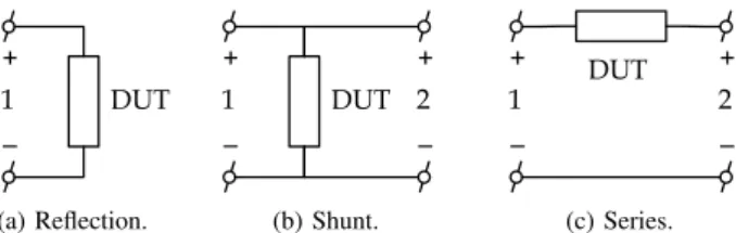
+ – 1 DUT (a) Reflection. + – 1 DUT + – 2 (b) Shunt. + – 1 DUT + – 2 (c) Series. Figure 1. All possible ways to connect a DUT to one and two ports.
II. DESIGN
We will now defend the choice of measurement configuration, substrate, connector and DUT footprint. A geometry optimisation and a sensitivity study under CST will be presented.
Below 3 GHz, one can measure impedances using impedance analysers, above, a VNA is preferred over an impedance analyser [2]. When measuring with a 2-port VNA, the device under test (DUT) can be connected to the analyser in three configurations, cf. Figure 1. The reflection configu-ration is relatively precise for impedances magnitudes around 50 Ω, the shunt configuration for small impedances, the series configuration for large impedances [3].
Our 1 nF capacitor nominally has an impedance between ±200 jΩ and 200 mΩ in the two decades around its 8 GHz resonance frequency. This pleads for a S21 shunt
measurement. To keep things simple, we choose the ‘reflection’ configuration, and we accept that we will not be able to measure the equivalent series resistance (ESR) very precisely; its nominal value is 200 mΩ. Another advantage of the ‘reflection’ configuration is, that it can also be mounted on an impedance analyser.
For simplicity, we try to design for a standard 1.55 mm FR-4 substrate. This substrate introduces higher losses than an RF-specific substrate. Therefore, we will try to keep the DUT and connector close together, so that the wave propagates only a small length through the dielectric. Furthermore, the losses will need to be assessed in simulation. Commonly, end-launch SMA connectors are used for ex-perimental printed circuit boards (PCBs). Their inconvenience
is that there generally needs to be about 6 mm between the board edge and the DUT.
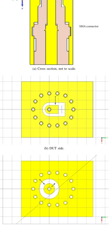
Alternatively, the Molex SD-73251-185 SMA connector is mounted perpendicular to the board. It is not soldered, but clamped to the board by means of screws [4]. A ring of ‘bolt’ vias and one central via emulate a coaxial connection through the board [5].
On the other side, the DUT will be clamped between the central via and the bolt vias, thus creating a non-coaxial fixture [2], i.e. the fixture is not point-symmetric around the connector’s axis. The resulting top and bottom footprints, as well as a cross section are depicted in Figure 2. As can be seen in Figure 2a, the rectangular soldermask gap on top of the PCB helps the operator to align the DUT.
To evaluate the performance of this fixture before manufac-turing, a CST simulation was performed. A waveguide port ‘1’ was defined on the SMA’s reference plane, and a discrete port ‘2’ was defined between the electrodes of a typical DUT. For the fixture to be transparent, its|S11| parameter must be low
and its|S21| parameter must be close to 0 dB. We sequentially
tuned the DUT footprint and the SMA footprint to approach these S -parameters, see the arrows in Figure 2b and 2c.
For measurement reproducibility, it is critical that the DUT placement (within the soldermask gap) does not change the S-parameters too much, because even a calibration cannot compensate this error. A sensitivity study was effectuated by displacing the DUT in x and y direction, and rotating slightly around the z axis, all as far as permitted by the soldermask gap. The results of this sensitivity study are presented in Figure 3a. Off smaller interest is the effect of the rather undefined relative permittivity of the FR-4 substrate, as its effect can be compensated by calibration. Yet, the S -parameters must not deviate too much from a transparent transmission line, because that makes the calibration less precise. We swept εrfrom 3.9 to
4.9, with a constant tan(δ) of 0.025. The results are presented in Figure 3b. The relatively low loss may be explained by the fact that the wave only travels 1.55 mm through the FR-4 substrate.
III. REALISATION
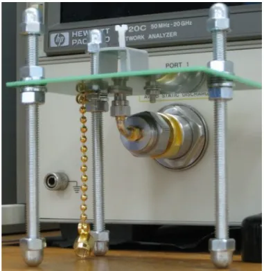
The fixture was fabricated in the standard 2-layer Eurocir-cuits process. The SMA connector was connected to the first port of an HP 8720C VNA (50 MHz–20 GHz) with a semi-rigid SMA 90◦bend. A spring with a nylon bolt on top was chosen to keep the DUT in place without impacting the electric field too much. See Figure 4.
IV. COMPENSATION
To obtain the impedance of the isolated component, we need to compensate the fixture’s influence on the measurement result. Three compensation methods will be compared.
The first and simplest method is subtracting an electrical delay from the measurements. That is, using
DUT soldermask
copper substrate copper
SMA connector
(a) Cross section, not to scale.
(b) DUT side.
(c) SMA side.
-1.50 -1.25 -1.00 -0.75 -0.50 -0.25 0.00 0 5 10 15 20 Frequency (GHz) |S21 | (dB) -30 -25 -20 -15 -10 -5 0 |S 11 | (dB) 3.9 4.3 4.9 S21 S11 -1.50 -1.25 -1.00 -0.75 -0.50 -0.25 0.00 0 5 10 15 20 Frequency (GHz) |S21 | ( d B ) -30 -25 -20 -15 -10 -5 0 |S 11 | ( d B ) S21 S11
(a) Sensitivity to DUT placement offset. Solid curve shows the response at the nominal DUT position. Non-solid curves show the response for ∆x = +0.1 mm, ∆y =±0.2mm and ∆θ = +10◦. -1.50 -1.25 -1.00 -0.75 -0.50 -0.25 0.00 0 5 10 15 20 Frequency (GHz) |S21 | (dB) -30 -25 -20 -15 -10 -5 0 |S 11 | (dB) 3.9 4.3 4.9 S21 S11 -1.50 -1.25 -1.00 -0.75 -0.50 -0.25 0.00 0 5 10 15 20 Frequency (GHz) |S21 | ( d B ) -30 -25 -20 -15 -10 -5 0 |S 11 | ( d B ) S21 S11
(b) Sensitivity to substrate permittivity.
Figure 3. Sensitivity study in simulation of the fixture’s S -parameters. Linear frequency scale to stress centimeter wave issues. The solid line consequently represents the nominal case.
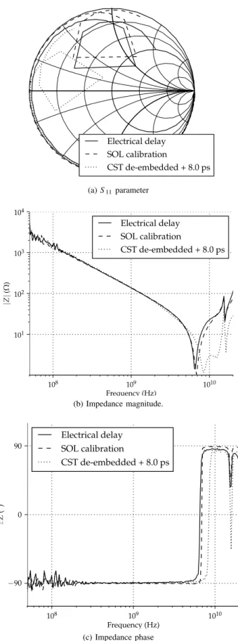
an Agilent 85052D SOL calibration kit (valid up to 26.5 GHz), the reference plane is shifted to the reference plane of the fixture’s SMA connector. Then, with no DUT in place, we search for the electrical delay that makes the phase of S11= 0◦over the whole bandwidth. We thus found 53.0 ps.
The second, more complicated method, is a SOL calibra-tion. The short standard is a 0603-sized 75% golden brick manufactured by the goldsmith. The open standard is simply the absence of a DUT. The load standard is a microwave 50 Ω resistor by Vishay [6].
If we consider these standards to be perfect, that is S11 ={−1,1,0}, the compensated S -parameters leave the
unit circle. We therefore look for more realistic models of our standards. Using an analytical model of a bar with rectangular cross section [7], we find its inductance to be 0.26 nH. Using an analytical model of the capacitance of two parallel straight wires, we calculate the excess stray capacitance, which will be replaced by the DUT, to be 7.3 fF. For the load, we use a LCLRC lumped element model [8].
(a) Overview: PCB with HP 8720C VNA
(b) Detail: spring-loaded nylon bolt keeps the DUT in place. Figure 4. Measurement set-up.
Finally, we tried to de-embed the measurement result using the CST-simulated S -parameters. That is, we use the Agilent 85052D calibration kit to move the reference plane to that of the fixture’s SMA connector. Using ADS, we de-embed the thus measured S -parameters with the simulated S-parameters. Note that we needed to add 8 ps electrical delay to the CST results, to match the measured open circuit response. We did not find a satisfactory explanation for this model shortage.
The compensated S - and Z-parameters are shown in Fig-ure 5. Supposing that the DUT behaves as a pFig-ure RLC series, the SOL-compensated result seems the most plausible, with a
resonance at 6.9 GHz.
Above 12 GHz, the behaviour can no longer be described with an RLC series. Either the RLC model is not competent above 12 GHz, or the calibration is not valid anymore, or both.
V. CONCLUSIONS
We developed a low-cost measurement fixture, that allows to measure the impedance of 0603-packaged SMDs up to about 12 GHz, when SOL calibration is used or a 53.0 ps electrical delay is subtracted.
When using a VNA, the impedance is most precise around 50 Ω, which allows to measure the resonant frequency, but prohibits measuring the ESR very precisely.
Using the fixture requires operator skills to manually align the SMD correctly. Furthermore, no metrological rigour was exercised to be able to define the measurement accuracy, so measurements taken with this fixture should be used as indication.
ACKNOWLEDGMENTS
We thank Jon Wiener and David Graham of Molex Incor-porated for their advise on the connector. We thank Richard Cousin of CST AG for his advise on the fixture simulations. We thank Dominique Vignolo of Vishay S.A. for supplying the lumped element model of the 50 Ω resistor.
REFERENCES
[1] Ultra Low ESR, “U” Series, C0G (NP0) Chip Capacitors, AVX. [Online]. Available: http://www.avx.com/docs/Catalogs/useriesrf.pdf [2] Impedance Measurement Handbook, 4th ed. Agilent, June 2009, no.
5950-3000. [Online]. Available: http://cp.literature.agilent.com/litweb/ pdf/5950-3000.pdf
[3] “Advanced impedance measurement capability of the RF I-V method compared to the network analysis method,” Agilent, Tech. Rep. 5988-0728, 2001. [Online]. Available: http://cp.literature.agilent.com/litweb/ pdf/5988-0728EN.pdf
[4] “Molex SD-73251-185 SMA jack, 2H flange with 0-80 thread, 50 ohm, 27 GHz,” Technical Drawing, Molex Incorporated, June 2010. [Online]. Available: http://www.molex.com/pdm docs/sd/732511850 sd.pdf [5] D. Dunham, “High speed SMA interface design,” CPD Connector
Divi-sion, Molex, Tech. Rep., June 2004.
[6] Thin film microwave resistors. Vishay Sfernice. [Online]. Available: http://www.vishay.com/docs/53014/ch.pdf
[7] E. Rosa, The self and mutual inductances of linear conductors, U. S. N. B. of Standards, Ed. US Dept. of Commerce and Labor, Bureau of Standards, 1908, vol. 4, no. 2.
[8] D. Vignolo, “Re: Request for 0603 wraparound (n) resistor model,” Email.
Electrical delay SOL calibration CST de-embedded + 8.0 ps (a) S11parameter 108 109 1010 Frequency (Hz) 101 102 103 104 |Z | (Ω ) Electrical delay SOL calibration CST de-embedded + 8.0 ps (b) Impedance magnitude. 108 109 1010 Frequency (Hz) −90 0 90 �Z ( ◦) Electrical delay SOL calibration CST de-embedded + 8.0 ps (c) Impedance phase
Figure 5. Measurement results of a 1 nF AVX capacitor, compensated using three different compensation techniques (electrical delay, SOL calibration and de-embedding using CST simulation results).