HAL Id: tel-01998527
https://pastel.archives-ouvertes.fr/tel-01998527
Submitted on 29 Jan 2019
HAL is a multi-disciplinary open access
archive for the deposit and dissemination of sci-entific research documents, whether they are pub-lished or not. The documents may come from teaching and research institutions in France or abroad, or from public or private research centers.
L’archive ouverte pluridisciplinaire HAL, est destinée au dépôt et à la diffusion de documents scientifiques de niveau recherche, publiés ou non, émanant des établissements d’enseignement et de recherche français ou étrangers, des laboratoires publics ou privés.
Modeling and characterization of materials and
nanostructures for photovoltaic application
Zuzana Mrazkova
To cite this version:
Zuzana Mrazkova. Modeling and characterization of materials and nanostructures for photovoltaic application. Micro and nanotechnologies/Microelectronics. Université Paris Saclay (COmUE); VŠB -Technical University of Ostrava, 2017. English. �NNT : 2017SACLX121�. �tel-01998527�
Th
`ese
de
doctor
at
NNT
:
2017SA
CLX121
Mod ´elisation et caract ´erisation de
mat ´eriaux et nanostructures pour les
applications photovolta¨ıques
Th `ese de doctorat de V ˇSB - Technical University of Ostrava et de l’Universit ´e Paris-Saclay, pr ´epar ´ee `a l’Ecole Polytechnique
Ecole doctorale n◦573 Interfaces : approches interdisciplinaires, fondements,
applications et innovation (Interfaces)
Sp ´ecialit ´e de doctorat : Physique
Th `ese pr ´esent ´ee et soutenue `a Ostrava, le 24 Novembre 2017, par
M
ME. Z
UZANAMRAZKOVA
Composition du Jury :
Jarom´ır Piˇstora
Professeur, V ˇSB - Technical University of Ostrava, Czech Republic Pr ´esident Kurt Hingerl
Professeur, Johannes Kepler Universit ¨at Linz, Austria Rapporteur Morten Kildemo
Professeur, Norwegian University of Science and Technology, Norway Rapporteur Janez Krˇc
Professeur, University of Ljubljana, Slovenia Rapporteur
Jean-Paul Kleider
Professeur, Universit ´e Paris-Saclay, France Examinateur
Pere Roca i Cabarrocas
Professeur, Universit ´e Paris-Saclay, France Directeur de th `ese Kamil Postava
Professeur associ ´e, V ˇSB - Technical University of Ostrava, Czech Republic Directeur de th `ese Martin Foldyna
École Polytechnique, Université Paris-Saclay
Laboratoire de Physique des Interfaces et des Couches Minces
and
VŠB - Technical University of Ostrava
University Study Programmes
Nanotechnology Centre
Modeling and characterization of materials and
nanostructures for photovoltaic applications
Thesis
Author: Ing. Zuzana Mrázková
Supervisor in France: Prof. Dr. Pere Roca i Cabarrocas
Co-supervisor in France: Ing. Martin Foldyna, Ph.D.
Supervisor in Czech Republic: Doc. Dr. Mgr. Kamil Postava
I declare I elaborated this thesis by myself. All literary sources and publications I have used had been cited.
Acknowledgements
I have done my PhD study in a frame of a student sharing programme “co-tutelle” in collaboration between two laboratories: Nanotechnology Centre at VŠB-Technical University of Ostrava in Czech Republic and Laboratoire de Physique des Interfaces et des Couches Minces, CNRS, École Polytechnique, Uni-versité Paris-Saclay in France. During this exceptional four-year period of my life I have met many kind colleagues and friends both in Czech Republic and in France. I would like to thank to each of you for all experiences we have shared. Each one has been important for me, nevertheless it was in the lab or office, dur-ing group meetdur-ings, coffe-breaks or lunch times...
I thank to directors of both involved laboratories, Jaromír Pištora and Pere Roca i Cabarrocas, who have enabled me to work in their labs, provided me fi-nancial support from projects and grants, and helped me to at least draw with if not directly to beat the bureaucracy.
I thank to supervisors of my thesis, Kamil, Pere, and Martin, for your guid-ance, advices and support. I have learned a lot of things of you. I appreciate your help with the scientific stuff and also with solving non-scientific issues. I am grateful for financial support from your projects as well as for the administra-tion of my join PhD study which has required a lot of paperwork. Thank you for guiding me through the exciting world of science.
Many thanks to my friends and colleagues who prepared samples for me and helped me with measurements. Thank you Igor, Soumyadeep, Mutaz, Letian, Jian, Ileana, Jean-Luc, and Ronan.
Tibor, Lukáš, Radek, Ondra, and Robin, thank you for being my friends to a disaster, for providing me an IT support and for having patience with my never-ending questions.
Many thanks to all my friends and colleagues from PVSiXT, Nanowire Team, and RP4 Supercomputing for Nanotechnologies research groups for being my friends and colleagues.
Especially thanks to my family and to my Martin for supporting me, rejoicing my successes and comforting me when things go wrong. Thank for always being here for me.
iii
Résumé
La recherche sur le photovoltaïque vise à réduire le prix par watt de puissance électrique générée. Des efforts considérables sont menés pour rechercher de nou-veaux matériaux et des conceptions qui repoussent les limites des cellules solaires existantes. Le développement récent de matériaux et nanostructures complexes pour les cellules solaires nécessite des efforts plus importants pour mener à bien leur caractérisation et leur modélisation. Cette thèse porte sur la caractérisation optique, la modélisation et l’optimisation de la conception d’architectures de cel-lules solaires de pointe.
La texturation des surfaces des cellules solaires est souvent utilisée pour amé-liorer le piégeage de la lumière, et donc améamé-liorer le rendement de conversion. Les textures pyramidales sont les plus utilisés pour le silicium cristallin, en rai-son de leur faible coût et leur facilité de fabrication. Leurs propriétés de piégeage de la lumière sont également bien documentées. Une autre approche pour amé-liorer l’absorption lumineuse et augmenter le rendement de conversion est d’in-corporer des nanostructures dans la conception des cellules. Les cellules solaires à base de jonction radiale de nanofils de silicium donnent une nouvelle perspec-tive pour les devices à couches minces nanostructurés, grâce à un piégeage de la lumière amélioré et le découplage entre la direction d’absorption de la lumière et celle dans laquelle les porteurs de charges sont collectés.
L’objectif de cette thèse est la caractérisation optique, la modélisation, et l’op-timisation des structures des cellules solaires fabriquées au Laboratoire de Phy-sique des Interfaces et des Couches Minces (LPICM). Cela inclut des études sur des cellules solaires fabriqués sur des wafers à texture pyramidale et sur des cel-lules solaires à jonction radiale de nanofils de silicium orientés aléatoirement. Nous démontrerons que les méthodes optiques sont bénéfiques pour la caracté-risation à la fois des textures pyramidales, et des nanofils de silicium.
Les mesures optiques sont utilisées pour la caractérisation rapide et non des-tructive des échantillons texturés pour les applications photovoltaïques. Les tex-tures de surface améliorent le piégeage de la lumière et sont donc souhaitées pour améliorer les performances des cellules solaires. D’autre part, ces textures rendent la caractérisation optique plus difficile et des efforts plus importants sont néces-saires non seulement pour la mesure optique elle-même mais également pour la modélisation et l’interprétation ultérieure des données obtenues. Dans ce travail, nous démontrons que nous sommes en mesure d’utiliser des méthodes optiques pour étudier les textures pyramidales très répandues ainsi que les réseaux de na-nofils de silicium à orientation aléatoire dont l’analyse est très difficile.
Premièrement, nous nous sommes concentrés sur l’étude optique de diverses surfaces pyramidales et de leur impact sur les performances des cellules silicium à hétérojonction. Nous avons constaté que les angles au sommet des pyramides,
iv
préparées à l’aide de différentes conditions de texturation, diffèrent de la
va-leur théorique de 70.52◦ attendue pour le silicium cristallin. Cette modification
de l’angle au sommet est expliquée par la présence, sur les facettes pyramidales, de terrasses monoatomiques régulières, observées par microscopie électronique à transmission de résolution atomique. L’impact d’une variation de l’angle au sommet sur les épaisseurs des couches minces déposées est étudié et les consé-quences sur l’efficacité des cellules solaires résultantes sont discutées. Un modèle optique développé pour le calcul de la réflectance et de l’absorption des couches minces en multicouches sur surfaces pyramidales a permis l’optimisation de la conception de la cellule solaire pour un angle au sommet pyramidal donné.
L’ellipsométrie matricielle Mueller a été utilisée in-situ pour caractériser les six premières minutes du processus de croissance - par méthode vapeur-liquide-solide activée par plasma - des nanofils de silicium. Les fonctions optiques du ZnO et de Sn ont été déterminées à partir de mesures optiques et de modèles des échantillons de référence. Nous avons développé un modèle optique facile à utiliser de la croissance sur des couches minces de ZnO de 1 µm d’épaisseur déposée sur du verre Corning, qui, à notre connaissance, est le premier modèle utilisant des données ellipsométriques expérimentales pour contrôler le procédé de croissance, en phase vapeur-liquide-solide assisté par plasma, des nanofils. La dépendance linéaire observée du dépôt de matériau de silicium avec le temps de dépôt nous permet de suivre le processus de fabrication in situ et de contrôler la qualité du matériau.
Mots clés: propriétés optiques ; ellipsométrie spectroscopique ; polarimétrie ma-tricielle Mueller in-situ ; modèles optiques multicouches ; cellules solaires silicium à hétérojonction ; textures pyramidales ; nanofils de silicium ; cellules solaires à jonction radiale
v
Abstract
Research in photovoltaics aims at lowering the price per watt of generated electrical power. Substantial efforts aim at searching for new materials and de-signs which can push the limits of existing solar cells. The recent development of complex materials and nanostructures for solar cells requires more effort to be put into their characterization and modeling. This thesis focuses on optical characterization, modeling, and design optimization of advanced solar cell archi-tectures.
Optical measurements are used for fast and non-destructive characterization of textured samples for photovoltaic applications. Surface textures enhance light-trapping and are thus desired to improve the solar cell performance. On the other hand, these textures make optical characterization more challenging and more effort is required for both, the optical measurement itself and subsequent modeling and interpretation of obtained data. In this work, we demonstrate that we are able to use optical methods to study the widely used pyramidal textures as well as very challenging randomly oriented silicon nanowire arrays.
At first, we focused on the optical study of various pyramidal surfaces and their impact on the silicon heterojunction solar cell performance. We have found that vertex angles of pyramids prepared using various texturing conditions vary
from the theoretical value of 70.52◦expected from crystalline silicon. This change
of the vertex angle is explained by regular monoatomic terraces, which are pres-ent on pyramid facets and are observed by atomic resolution transmission elec-tron microscopy. The impact of a vertex angle variation on the thicknesses of deposited thin films is studied and the consequences for resulting solar cell effi-ciency are discussed. A developed optical model for calculation of the reflectance and absorptance of thin film multi-layers on pyramidal surfaces enabled a solar cell design optimization, with respect to a given pyramid vertex angle.
In-situ Mueller matrix ellipsometry has been applied for monitoring the sil-icon nanowire growth process by plasma-enhanced vapor-liquid-solid method. We have developed an easy-to-use optical model, which is to our knowledge a first model fitting the experimental ellipsometric data for process control of plasma-assisted vapor-liquid-solid grown nanowires. The observed linear de-pendence of the silicon material deposition on the deposition time enables us to trace the fabrication process in-situ and to control material quality.
Keywords: optical properties; spectroscopic ellipsometry; in-situ Mueller matrix polarimetry; multi-layer optical models; silicon heterojunction solar cells; pyra-midal texture; silicon nanowires; radial junction solar cells
vi
Abstrakt
Cílem výzkumu v oblasti fotovoltaiky je snížit cenu za watt vyrobené elek-trické energie. Znaˇcné úsilí se vˇenuje hledání nových materiál ˚u a struktur, které umožní posunout hranice stávajících solárních ˇclánk ˚u. Neustálý pokrok ve vý-voji materiál ˚u a nanostruktur pro solární ˇclánky zvyšuje nároky také na jejich charakterizaci a modelování. Tato práce se zamˇeˇruje na optickou charakterizaci, modelování a optimalizaci návrh ˚u pokroˇcilých struktur solárních ˇclánk ˚u.
Optické metody jsou vhodné k rychlé a nedestruktivní charakterizaci textu-rovaných vzork ˚u pro fotovoltaické aplikace. Povrchové textury, které umož ˇnují lepší zachycení svˇetla a jsou proto žádoucí pro zlepšení úˇcinnosti solárních ˇclán-k ˚u, bohužel znesnad ˇnují opticˇclán-kou charaˇclán-kterizaci. Je tedy zapotˇrebí vˇetšího úsilí jak pro realizaci samotných optických mˇeˇrení, tak pro následné modelování a interpretaci získaných dat. V této práci demonstrujeme, že jsme schopni použít optické metody ke studiu široce používaných pyramidálních textur, tak i ménˇe obvyklých, na charakterizaci nároˇcných, náhodnˇe orientovaných kˇremíkových nanodrátk ˚u.
Nejprve jsme se zamˇeˇrili na optické studium r ˚uzných pyramidálních povr-chových textur a jejich vlivu na úˇcinnost solárních ˇclánk ˚u s kˇremíkovým hetero-pˇrechodem. Zjistili jsme, že vrcholové úhly pyramid pˇripravených r ˚uznými
tex-turovacími procesy se liší od teoretické hodnoty 70.52◦ vycházející z
krystalogra-fie kˇremíku. Tuto zmˇenu vrcholového úhlu vysvˇetlujeme pˇrítomností pravidel-ných monoatomických teras na stˇenách pyramid, které jsme pozorovali pomocí transmisní elektronové mikroskopie s atomovou rozlišovací schopností. Provedli jsme studii vlivu zmˇeny vrcholového úhlu na tloušt’ky nanesených ten-kých vrstev a diskutovali jsme možné d ˚usledky pro výslednou úˇcinnost solárních ˇclánk ˚u. Vyvinuli jsme optický model pro výpoˇcet odrazivosti a absorpce tenko-vrstevných systém ˚u na pyramidách, jenž nám umožnil optimalizaci vrstev na povrchu solárních ˇclánk ˚u s ohledem na vrcholový úhel daných pyramid.
In-situ elipsometrie Muellerovy matice byla použita pro sledování r ˚ustu kˇre-míkových nanodrátk ˚u metodou plasma-assisted vapor-liquid-solid. Vyvinuli jsme snadno použitelný optický model, který je, pokud víme, prvním mode-lem pro analýzu ellipsometrických dat mˇeˇrených pˇrímo v reaktoru bˇehem r ˚ustu náhodnˇe orientovaných kˇremíkových nanodrátk ˚u. Pozorovaná lineární závislost depozice kˇremíku na ˇcase nám umož ˇnuje in-situ monitorování výrobního pro-cesu a kontrolu kvality materiálu.
Klí ˇcová slova: optické vlastnosti; spektrální elipsometrie, in-situ polarimetrie Muellerovy matice; multivrstevné optické modely; solární ˇclánky s kˇremíkovým heteropˇrechodem; pyramidální textury; kˇremíkové nanodrátky; solární ˇclánky s radiálním polovodiˇcovým pˇrechodem
Contents
Acknowledgements i Abstracts iii Contents vii List of symbols ix 1 Introduction 1 1.1 Photovoltaic applications. . . 41.2 State of the art . . . 6
1.3 Objective of the work . . . 9
1.4 Organization of the thesis . . . 10
2 Sample preparation 11 2.1 Silicon heterojunction solar cells. . . 12
2.1.1 Description of textured wafers . . . 14
2.2 Radial junction solar cells . . . 14
2.2.1 Silicon nanowires grown for radial junction solar cells . . . . 16
3 Characterization methods 19 3.1 Total reflectance and transmittance measurements . . . 20
3.2 Standard and Mueller matrix ellipsometry. . . 20
3.2.1 Standard spectroscopic ellipsometry . . . 21
3.2.2 In-situ spectroscopic Mueller matrix ellipsometry . . . 22
3.2.3 Angle-resolved Mueller matrix ellipsometry . . . 23
4 Theoretical background 25 4.1 Electromagnetic theory of light . . . 26
4.1.1 Maxwell equations in general medium . . . 26
4.1.2 Classification of material media . . . 27
4.1.3 Electromagnetic waves in non-absorbing medium . . . 30
4.1.4 Electromagnetic waves in absorbing medium . . . 32
4.2 Light propagation in thin film systems . . . 34
4.2.1 Yeh’s matrix formalism . . . 35
4.2.2 Optical intensity and power . . . 40
viii CONTENTS
4.3 Principles of ellipsometric techniques . . . 44
4.3.1 Principles of spectroscopic ellipsometry . . . 45
4.3.2 Principles of Mueller matrix polarimetry . . . 46
4.3.3 Data analysis . . . 48
5 Results for pyramidal textured samples 53 5.1 Reflectance of pyramidal textured surfaces . . . 54
5.2 Analysis of angles of pyramids . . . 59
5.2.1 Measurement of the angles of pyramids . . . 59
5.2.2 Origin of different pyramidal angles . . . 63
5.3 Analysis of thin films on pyramids . . . 64
5.3.1 Consequences of vertex angle variation . . . 64
5.3.2 Model of spectroscopic ellipsometry data. . . 65
5.3.3 Optimization of multi-layer system . . . 71
5.3.4 Silicon heterojunction solar cells . . . 73
5.4 Chapter key results . . . 75
6 Results for silicon nanowires 77 6.1 Characterization of used materials . . . 78
6.2 Substrate characterization before nanowire growth. . . 85
6.3 In-situ characterization of silicon nanowire growth. . . 88
6.4 Ex-situ characterization after nanowire growth . . . 95
6.5 Chapter key results . . . 97
Conclusions and perspectives 99 Conclusions . . . 99
Perspectives . . . 99
A Optical functions of materials 101 Intrinsic hydrogenated amorphous silicon (i)a-Si:H . . . 102
Intrinsic hydrogenated amorphous silicon carbide (i)a-SiC:H. . . 103
P-type hydrogenated amorphous silicon (p)a-Si:H and (p++)a-Si:H . . . . 106
Indium tin oxide ITO. . . 107
List of figures 111
List of tables 115
List of publications 117
ix
List of symbols
AR Anti-Reflective, Anti-Reflection
AR-MMP Angle-Resolved Mueller Matrix Polarimetry
B-EMA Bruggeman Effective Medium Approximation
CVD Chemical Vapor Deposition
FTO Fluorine-doped Tin Oxide
IPA Isopropyl Alcohol
ITO Indium Tin Oxide
JV current density-voltage
LPICM Laboratoire de Physique des Interfaces et des Couches Minces
NIR Near-Infrared
NW Nanowire
PECVD Plasma-Enhanced Chemical Vapor Deposition
PV Photovoltaic
SE Spectroscopic Ellipsometry
SEM Scanning Electron Microscopy
SHJ Silicon Heterojunction
SiNW Silicon Nanowire
STEM-BF Scanning Transmission Electron Microscopy in Bright-Field
STEM-HAADF Scanning Transmission Electron Microscopy in High-AngleAnnular Dark-Field
TCO Transparent Conducting Oxide
TEM Transmission Electron Microscopy
TMB Trimethylboron
UV Ultraviolet
Vis Visible
VLS Vapor-Liquid-Solid method
a-Si:H hydrogenated amorphous silicon
a-SiC:H hydrogenated amorphous silicon carbide
(i)a-Si:H intrinsic hydrogenated amorphous silicon
(i)a-SiC:H intrinsic hydrogenated amorphous silicon carbide
(n+)a-Si:H n-type hydrogenated amorphous silicon
(p)a-Si:H p-type hydrogenated amorphous silicon with low doping level
(p++)a-Si:H p-type hydrogenated amorphous silicon with high doping level
c-Si crystalline silicon
(n)c-Si n-type crystalline silicon
uc-Si microcrystalline silicon
x LIST OF SYMBOLS
× cross product
∇· divergence operator
∇× curl operator
h.i time period average
ℜ real part ℑ imaginary part i imaginary unit ∗ complex conjugate ⊗ Kronecker product A amplitudes vector
A(i) amplitudes vector in i-th layer
A absorptance
AC, BC, CC fitting parameters of Cauchy transparent model
AL oscillator amplitude
AM 1.5G global standard solar spectrum at the Earth’s surface
AOI angle of incidence
B(r, t) magnetic flux density
C oscillator broadening
c light speed in free space
D(r, t) electric displacement
D(i) dynamic matrix of i-th layer
d distance, thickness
E(r, t) electric field vector
Eω(r) complex amplitude of electric field
E0 electric field complex envelope
E photon energy
Eg energy band gap
Ep plasma energy
EL,0 oscillator position
e electric field polarization vector
F F fill factor
fj volume fraction of j-th material
H(r, t) magnetic field vector
Hω(r) complex amplitude of magnetic field
H0 magnetic field complex envelope
h magnetic field polarization vector
bI identity matrix
I optical intensity
xi
J Jones matrix
Jph loss loss in photo-generated current density
JSC short-circuit current density
j(r, t) current density vector
k imaginary part of refractive index
L layer thickness
M Mueller matrix
M total matrix of thin film system
M(r, t) magnetization vector
M number of spectral points
N number of fitting parameters
Nx, Ny, Nz propagating constants
N A numerical aperture
n real part of refractive index
˜
n complex refractive index
bn complex tensor of refractive index
P(r, t) polarization vector
P(i) propagation matrix of i-th layer
P Cauchy principal value
P pyramid geometrical factor
PD depolarization index
p thickness of gradient p-type layer
q electron charge
R reflectance
r amplitude reflection coefficient
r space position vector
S Stokes vector
S Poynting vector
Sω complex Poynting vector
T transmittance
t time, amplitude transmission coefficient
u unit normal vector
VOC open circuit voltage
v light speed in medium
x, y, z space coordinates
xii LIST OF SYMBOLS
α pyramid vertex angle, absorption coefficient
β pyramid side angle
ΓD collision frequency of free carriers
γ emerging angle
γL oscillator damping
γS factor related to a screening and a shape of inclusions
∆ ellipsometric phase angle
δ absolute phase change
ε electric permitivity, dielectric function
b
ε electric permitivity tensor
˜
ε complex electric permitivity
ε(i) complex relative permitivity of i-th medium
εr relative electric permitivity
b
εr relative permitivity tensor
˜
εr complex relative permitivity
ε0 free space electric permitivity
ε1 real part of complex relative permitivity
ε2 imaginary part of complex relative permitivity
ε∞ high-frequency dielectric constant
η impedance of medium
η0 impedance of free space
θ phase shift ϑ polar angle κ wave vector κ wavenumber ˜ κ complex wavenumber
κ0 wavenumber in free space
λ wavelength
µ magnetic permeability
b
µ magnetic permeability tensor
µr relative magnetic permeability
b
µr relative permeability tensor
µ0 free space magnetic permeability
ν frequency
ρ(r, t) charge volume density
ρS degree of light polarization
σ electric conductivity
b
σ electric conductivity tensor
σSD standard deviation
xiii
ϕ angle of incidence, angle of propagation
φ azimuthal angle
χe electric susceptibility
b
χe electric susceptibility tensor
χm magnetic susceptibility
b
χm magnetic susceptibility tensor
χ2 fitting error function
Ψ ellipsometric amplitude angle
1
1
Introduction
Outline
1.1 Photovoltaic applications . . . 4 1.2 State of the art. . . 6 1.3 Objective of the work . . . 9 1.4 Organization of the thesis. . . 10
2 CHAPTER 1. INTRODUCTION Energy is an essential element to ensure human life needs. We need energy to produce and supply food and clean water. We need it for heating, to ensure health care and security. We use energy every day to improve our life well-being. Figure 1.1 shows the world consumption of primary energy per capita in tonnes of oil equivalent in 2014.
Figure 1.1 – World primary energy consumption per capita in tonnes of oil equiv-alent in 2014. This figure was adapted from Ref. 1.
World energy consumption is driven by two divergent driving forces. Rapid growth and improving prosperity mean the growth in energy demand mainly in fast developing economies, particularly in Asia. On the contrary, improve-ment of energy efficiency thanks to technological developimprove-ments decelerates the increase of global energy consumption. As a result, energy consumption still grows but the growth has slowed down in recent years. The growth was only 1 % or less during last three years [2]. Furthermore, the energy mix is shifting towards cleaner, lower carbon fuels. This trend is driven by environmental needs and allowed by technological advances. The shift is well-documented by a sharp decrease of coal consumption in two last consecutive years (-1.7 % in 2016 [2]) and by a strong increase in renewable energy use. Renewable power, led by wind (in-creased by 15.6 %, 131 TWh in 2016) and solar (increase of 29.6 %, 77 TWh in 2016), is the fastest growing energy source (increase of 12 % in 2016 [2]), account-ing for almost a third of the increase in primary energy, despite havaccount-ing a share of only 4 % of it [2].
3 Renewable energy is now a key element of sustainable development strate-gies which, among others, address climate change and provide health benefits compared with fossil fuels [3]. Unlike fossil fuels, renewable energy sources such as solar or wind energy are virtually unlimited. The advantage of using the solar energy stands from its presence anywhere in the world, without limitations or the dependence imposed by the strategic location of scarce fossil or nuclear fuels. The current trend of harvesting the energy from the Sun tends towards the photovoltaic (PV) devices which can directly convert the solar energy into elec-tricity. Photovoltaics has already accounted for about 2 % of global electricity in 2016 [3]. Moreover, the integration of PV into electricity system has reached 10-20 % in some countries such as Germany, Italy or Samoa [3]. The PV is the fastest growing sector of electricity generated from renewable sources. Its power capacity increased by 31.5 % and reached 295 GW in 2016 which accounts for 44 % of the increase in total electric capacity from renewable sources [4]. PV now represents more than half of all investment in the renewable energy sector [3].
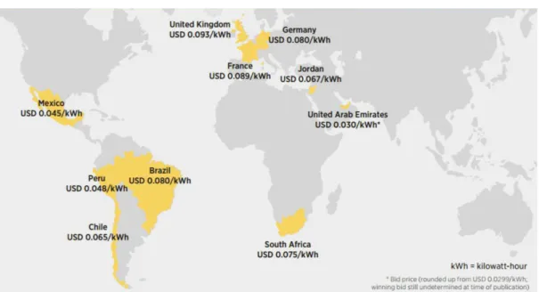
The rapid diffusion of PV is supported by new technologies which make bet-ter performance available at lower cost. The cost reduction was dramatic in few past years and PV became cost-competitive with electricity from conventional sources. The levelized cost of electricity for utility-scale PV was typically between 6 and 10 US cents (USD 0.06-0.10) per kilowatt-hour (kWh) in Europe, China, In-dia, South Africa and USA in 2015. Record low prices below USD 0.06/kWh were set in 2015 in United Arab Emirates (USD 0.0584/kWh), Peru (USD 0.048/kWh), and Mexico (USD 0.045/kWh) [3]. The price under three cents (USD 0.0299/kWh) was achieved in Dubai in 2016 [3]. Figure 1.2 shows prices of utility-scale solar PV in key markets in 2015. In comparison, the electricity production from coal- and gas-fired power stations was in the range of USD 0.05-0.10/kWh in 2015 [3]. Mo-rover, there is also a big expansion in rooftop PV installations, which can provide electric power at lower cost than the grid in many countries.
Not only the cost of electricity but also the cost of building PV plant is nowa-days close to or lower than that of conventional power plant [3]. Building utility-scale PV system can thus be cheaper and much faster than building new gas- or coal-fired power stations.
Another often mentioned draw-back, the energy pay-back (the time needed for a PV panel to produce energy used for its fabrication), has also been ad-dressed. The energy pay-back has been reduced down to 2 years or less [3] (de-pending on location) by improvements in resource use, manufacturing process and efficiency.
The significant cost reduction is certainly the primary driver for PV diffusion. However, there are also other aspects. The transfer of PV technology is not lim-ited by strict security restrictions in contrast with nuclear power. Furthermore,
4 CHAPTER 1. INTRODUCTION
Figure 1.2 – Prices of utility-scale solar PV in key markets in 2015. This figure was adapted from Ref. 3.
by 200-300 million tonnes per year [3]. Photovoltaics together with other renew-ables provide major health benefits compared to fossil fuels.
1.1
Photovoltaic applications
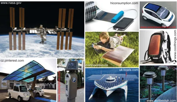
Large area power plants usually come into the mind first when thinking about PV systems. However, the PV applications are much broader. Apart from the utility-scale PV stations, rooftop PV systems, building integrated PV and rural electrification of areas that are off grid, there are many other areas in which PV is used. Examples of various PV applications are illustrated in Fig. 1.3.
There is a long tradition of using PV for spacecraft applications. In fact this was one of the earliest PV applications. PV panels are installed on satellites, probes and on the International Space Station. They provide power for sen-sors, heating and cooling, communication systems etc. The crucial parameters for spacecraft systems are the power generated per kilogram and stability under extreme space conditions. Therefore high-efficiency but more expensive panels based on advanced designs and III-V semiconductors are preferred [5].
Photovolatic panels can also be integrated to vehicles such as cars, boats and even airplanes. They can be used to charge the electric vehicles or just as an additional power supply for smaller systems, for example air-conditioning. The cost and efficiency are usually the most important parameters of PV panels for
1.1. PHOTOVOLTAIC APPLICATIONS 5 these applications, as well as the weight, durability, and flexibility which allows the integration of panels.
Various PV modules and mini-modules are used in solar powered standalone devices. There are plenty of them from well-known calculators and watches, through solar lamps, temporary traffic signs, parking meters, to water pumps or remote sensors of environment. The price plays the key role for these applica-tions, while the generated power and size can be smaller.
Another field of applications is represented by solar chargers reaching from large charging stations for vehicles through portable standalone devices of vari-ous sizes to chargers integrated to bags or clothes.
www.nasa.gov hiconsumption.com w w w .co o lt h in g s. co m pvinnovation.ca www.solarpoweredcars.net uk.boats.com w w w .i st o ckp h o to .co m www.doitbestgh.com cz.pinterest.com
Figure 1.3 – Examples of PV applications. Sources of particular images are indi-cated within the figure.
Various applications have various demands on PV module properties such as cost, efficiency, weight, size, durability, flexibility, mobility etc. Fortunately, there are many different PV technologies to choose from according to preferred properties.
The PV market is dominated by crystalline silicon (c-Si) technology. It ac-counts for about 90% [6] of market and it is usually the choice for utility-scale PV power plants and rooftop systems. It has undergone a long evolution and it approaches its theoretical efficiency limit of about 29% [3]. Thin film technologies such as hydrogenated amorphous silicon (a-Si:H), cadmium telluride, or copper indium gallium selenide benefit from reduced thickness (0.6 − 3 µm in contrast to 180 µm thick c-Si wafers). This leads to material and cost savings and opens
6 CHAPTER 1. INTRODUCTION new set of applications. Then, there are low-cost alternatives such as perovskites which exhibit reasonable good efficiency (22.1% [7]) but their problems with en-vironmental stability and sensitivity to moisture have to be solved. The lower efficiency of organic (11.5% [7]) and dye-sensitised (11.9% [7]) PV cells is com-pensated by their lightweight, flexibility and relatively cheap production.
1.2
State of the art
The research in photovoltaics aims at lowering the price per watt of generated electrical power. This can be achieved by increasing the conversion efficiency of solar cells and by lowering their fabrication cost. Substantial efforts aim towards searching for new materials and designs which can push the limits of existing solar cells.
Surface texturing of solar cells is usually used to enhance light trapping and thus improves the conversion efficiency. The most widely used textures for crys-talline silicon are pyramidal ones, since they are easy to fabricate at relatively low cost, while exhibiting well-documented light-trapping properties [8, 9].
Silicon heterojunction (SHJ) solar cells are an example of advanced architec-tures built on pyramidal textured wafers. They combine high efficiencies (24.7 % achieved already in 2014 [10]) with relatively low-cost fabrication thanks to the
process temperatures below 200◦C. The SHJ structure was further improved by
adding a thin intrinsic buffer layer leading to the heterojunction with intrinsic thin layer structure [11]. Panasonic pushed the limit to 25.6 % in 2014 by com-bining the SHJ concept with the interdigitated back-contact architecture [12]. A new efficiency record of 26.6 % for a practical size crystalline silicon solar cell has been achieved by Kaneka in 2016 [13], thanks to a combination of heterojunc-tion technology using high-quality amorphous silicon, a low resistance electrode technology, and a back-contact structure that captures more light.
Another approach to enhance light absorption and to increase the conver-sion efficiency is incorporating nanostructures into the solar cell design. Silicon nanowire (SiNW) based radial junction solar cells open a new direction for nanos-tructured thin film devices due to their enhanced light trapping and decoupling of the direction in which light is absorbed from that in which charge carriers are collected [14, 15]. Radial junction devices can be fabricated using thin film de-position (forming radial junction) on the top of SiNW arrays grown by plasma-assisted vapor-liquid-solid (VLS) process [16]. This allows the use of thinner ac-tive layers [light trapping is strongly dependent on nanowire (NW) lengths] and the reduction of the carrier collection path (small radius of radial junctions). Be-cause of the used low-melting point Sn as a catalyst, this method allows the fabri-cation of devices in a one-pump-down process with temperatures not exceeding
1.2. STATE OF THE ART 7
425◦C. This reduces the fabrication cost and opens the possibility to use low-cost
substrates such as glass, flexible foils or even plastics [15]. An efficiency of 9.2 % was demonstrated for radial junction solar cells built over VLS-grown SiNWs with 100 nm thick intrinsic hydrogenated amorphous silicon [(i)a-Si:H] absorber on glass substrates [17].
The most recent development of complex materials and nanostructures for solar cells requires more effort to be put into their characterization and model-ing. Optical methods are powerful characterization techniques, since they are fast, non-destructive, and non-invasive. Moreover, they can provide a lot of valu-able information not only about the sample optical properties but also about their structure. Some optical measurements can be carried out even in-situ in the re-actor and enable thus real-time monitoring of the sample during the fabrication process.
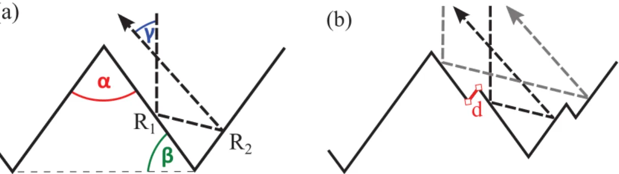
Monocrystalline silicon wafers are most commonly textured in an alkaline etching solution leading to a random array of upright pyramids on the etched surface [18–20]. The final morphology of the features has various implications for the performance of silicon solar cells. Front-surface reflectance, light-trapping capacity, module performance and surface recombination may all be affected [21]. Studies on pyramidal textured wafers (for example see [19, 22]) typically
ex-pect the pyramid vertex angle α = 70.52◦ and base angle β = 54.74◦ as a result
of ideal {111} facet intersection. In contrast, careful examination of the features often reveals otherwise [23, 24]. Base angle of the texture depends on the etching solution and varies in the range of 49◦− 52◦ [21,25]. However, relatively few
con-clusions have been transferred into the analysis of surface texture in silicon solar cell applications.
The deviation from the ideal morphology is given to relation with the limited etching selectivity [26], but the precise mechanism remains questionable. Two proposed contributors are as follows: (i) the exposure of a convex corner of the growing feature results in the etching of higher index beveling planes that even-tually intersect to form a stable bowed facet, and (ii) the formation of terrace-like structures on the pyramid facet as etching proceeds [23, 24, 27–29]. Given that the texture morphology evolves as the composition of an etch bath changes, a method for characterization of the evolving morphology is a critical requirement for the precise process control [21].
Pyramid geometry is particularly critical to the modeling and performance of the textured solar cells. The deviation from the ideal structure has numerous implications for silicon solar cell design, characterisation and modelling. Anal-yses of anti-reflection, light trapping, photogeneration and surface recombina-tion properties of textured surfaces should take this feature morphology into ac-count [21].
8 CHAPTER 1. INTRODUCTION ray-tracing calculus [30] are typically applied to describe reflection of incident light from pyramidal textured samples. Another approach for the calculation of reflectance and transmittance of textured silicon were introduced in [31]. It is based on the general expression for the reflectance of a pyramidal texture de-duced from identification of discrete paths of the reflection and the fraction of reflected light that follows each of these paths. The fractions were determined again by geometrical ray-tracing. The analysis was extended to determine also the transmittance of the structure to allow optimization of the thickness of anti-reflective coatings. This approach still involves rather complex calculations and is far from an easy-to-apply method. In addition, the analysis doesn’t take into account the real geometry of pyramids but employs the ideal one.
The precise control of thickness of deposited films (passivating and doped layers, anti-reflective coatings etc.) is crucial to obtain the designed solar cell architecture. Spectroscopic ellipsometry is a suitable method for film thickness characterization, since it is non-destructive, high-precision and extremely sensi-tive to the properties of interfaces and thin films. However, reduced reflectivity and high scattering of the textured surfaces which are desired for PV applications make the ellipsometric characterization rather challenging.
Spectroscopic ellipsometry measurements of pyramidal textured samples re-quire an increased light source intensity and specific measurement configuration to obtain ellipsometric signal with a good signal to noise ratio [8]. Saenger et
al. [9] proposed a method for spectroscopic ellipsometry measurements of SiNx
anti-reflective coatings on pyramidal textured wafers. They tilted the sample to align pyramid facets perpendicularly to the plane of incidence. Conventional flat optical model can be used for data analysis thanks to the measurement of the specular reflection from inclined pyramid facets. Watanabe et al. [32] applied this technique for thickness characterization of hydrogenated amorphous silicon on pyramids for silicon heterojunction solar cells. Matsuki et al. [33] used this technique for characterization of multi-layers on pyramids. They were able to determine not only the thicknesses but also the hydrogen content in a-Si:H film and carrier properties in indium tin oxide layer from ellipsometric data.
Spectroscopic reflectometry and ellipsometry are also suitable techniques to monitor processes during solar cell fabrication. Real-time spectroscopic ellip-sometry is advantageously used for the monitoring and study of the growth of amorphous and microcrystalline silicon thin films [34–38]. However, using these methods for characterization of SiNW growth is much more challenging.
An in-situ spectroscopic ellipsometer module integrated in a plasma-enhanc-ed chemical vapor deposition (PECVD) reactor was usplasma-enhanc-ed by Yu et al. [39] to moni-tor in real time the optical response evolution of the SiNW structure. They traced the evolution of the intensity of light reflected from the sample surface and as-sessed the decrease in the reflected intensity to the enhanced light-trapping effect
1.3. OBJECTIVE OF THE WORK 9 during the growth of SiNW structure. However, they didn’t model the ellipso-metric data and a complete optical model representing the complex SiNW struc-ture is still needed.
1.3
Objective of the work
The objective of this thesis is optical characterization, modeling, and struc-ture optimization of advanced solar cell architecstruc-tures fabricated in Laboratoire de Physique des Interfaces et des Couches Minces (LPICM). This includes study of silicon heterojunction solar cells fabricated on pyramidal textured wafers and radial junction solar cells built on randomly oriented silicon nanowires. We will demonstrate that optical methods are beneficial for characterization of both, wide-ly used pyramidal textures as well as very challenging silicon nanowires.
Optimization of multi-layers in the heterojunction and fine tuning of pyrami-dal texture by etching processes is often performed by trial-and-error, without detailed analysis of the reasons for improved or reduced optical performance. Moreover, the geometry of pyramids is usually not verified and the ideal one re-sulting from the crystalography of silicon is assumed. This thesis focuses on a deeper study and understanding of the differences between various pyramidal textures and their impact on the solar cell design, fabrication, and performance.
The control of the SiNW growth process is essential for further improvement of the radial junction solar cell performance. The quality of deposition can be con-trolled by the characterization of materials and nanostructures during the growth process using an in-situ ellipsometry. Development of models able to describe and characterize the structure during the growth is highly desired. The model for the in-situ characterization is not always straight-forward, because some material properties as well as surfaces of deposited materials change during the growth. In this thesis, data obtained during SiNW sample fabrication will be analyzed to monitor the deposition process. The ultimate goal is the design of a model for the quality control of the growth process by means of in-situ ellipsometry.
To sum up, the focus of this thesis is on developing optical models adapted for the characterization of the photovoltaic devices, the quantitative criteria for the control of the quality of materials from different fabrication steps, and investi-gation of novel materials and nanostructures used to increase energy conversion efficiency of solar cells.
10 CHAPTER 1. INTRODUCTION
1.4
Organization of the thesis
The thesis is organized into following chapters:
Chapter 2 provides information on the preparation of studied samples. The
fabrication of silicon heterojunction solar cells by plasma-enhanced chemical va-por deposition is described together with the etching processes used to create pyramidal textures on silicon wafers. The radial junction solar cell fabrication is introduced, including the description of plasma-assisted vapor-liquid-solid method for growth of randomly oriented silicon nanowires.
Chapter 3introduces methods used for sample characterization. Measurement
set-up for total reflectance and transmittance measurements as well as for various ellipsometric techniques are described.
Chapter 4 provides the theoretical background for the optical modeling. First,
the electromagnetic theory of light is introduced. Then, the formalism describing light propagation in thin film systems is derived from the electromagnetic the-ory. Finally, principles of ellipsometric techniques are described and data analysis based on optical modeling of thin film systems is explained.
Chapter 5summarizes results for pyramidal textured samples. The impact of
various pyramidal textures on the total reflectance is studied. An easy-to-use model for reflectance from pyramidal surface is designed. Analysis of angles of real pyramids is performed, an explanation for the origin of the deviation from the ideal values is proposed, and consequences for thin film deposition and solar cell performance are discussed. The spectroscopic ellipsometry is employed for precise characterization of thicknesses of thin films on pyramids and an optical model for the optimization of thin-film systems on pyramidal textured wafers is designed. The importance of a precise control of the deposited film thicknesses is demonstrated on JV characteristic of final device.
Chapter 6shows results of a study of silicon nanowire growth. First, the
char-acterization of used materials is performed and obtained optical functions are adapted to correspond to the conditions in the reactor during fabrication process. Then, characterization of substrate before nanowire growth is carried out and suitable optical model is designed and verified. Finally, silicon nanowire growth is studied using ellipsometric data measured in-situ during the process. Multi-layer optical model is designed and evolved to describe changing structure of the sample. Trends obtained from data modeling are analyzed.
11
2
Sample preparation
Outline
2.1 Silicon heterojunction solar cells . . . 12
2.1.1 Description of textured wafers . . . 14
2.2 Radial junction solar cells . . . 14
12 CHAPTER 2. SAMPLE PREPARATION Samples of silicon heterojunction solar cells on pyramidal textured wafers were prepared in Laboratoire de Physique des Interfaces et des Couches Minces using plasma-enhanced chemical vapor deposition. Randomly oriented silicon nanowires which act as basis for radial junction solar cells were grown by plasma-assisted vapor-liquid-solid method in the same laboratory. I cooperated with my colleagues: Igor Sobkowicz, Soumyadeep Misra, Mutaz Al-Ghzaiwat, and Letian Dai, who processed the samples and did depositions, while I worked on sample characterization and processing and modeling of measured data.
2.1
Silicon heterojunction solar cells
Figure 2.1 shows the structure of a SHJ solar cell built on a pyramidal textured crystalline silicon wafer and the sample with finalized SHJ solar cells. N-type tex-tured c-Si (n)c-Si wafers of thickness around 230 µm and resistivity of 2.6 Ω · cm were used as substrates. The fabrication of SHJ solar cells includes the deposi-tion of intrinsic and doped hydrogenated amorphous silicon by low-temperature PECVD, the deposition of indium tin oxide (ITO) by magnetron sputtering at 180◦C, and the evaporation of silver contacts.
Ag Ag ITO (p++)a-Si:H (p)a-Si:H (i)a-Si:H (i)a-SiC:H (i)a-Si:H (n+)a-Si:H ITO Ag (n)c-Si ~ 230µm 2.6 ·cm (a)
Figure 2.1 – Single heterojunction solar cells built on a pyramidal textured c-Si wafer. (a) Schematic drawing (the structure is not drawn to scale) and (b) photo
of a sample with 2x2 cm2 and 1x1 cm2 SHJ solar cells.
Plasma-enhanced chemical vapor deposition is a process which enables depo-sition of thin films of various materials from a gas precursors onto substrates at lower temperature than that of a standard chemical vapor deposition (CVD) [40]. In PECVD process electron energy (plasma), instead of thermal energy (heat), is used to start the chemical reaction of gas precursors [41]. Plasma will ionize and decompose reactant gases leading to much lower deposition temperatures
2.1. SILICON HETEROJUNCTION SOLAR CELLS 13
600 − 1200◦C) [41]. The lower deposition temperatures are critical in many
ap-plications, where CVD temperatures could damage the devices being fabricated. Furthermore, low deposition temperatures are desirable for industrial production since they reduce fabrication costs.
Plasma-enhanced chemical vapor deposition of thin films for SHJ devices at 200◦C includes: deposition of thin intrinsic a-Si:H [(i)a-Si:H] films on both sides
of the textured wafer, deposition of n-type a-Si:H layer [(n+)a-Si:H] for the back surface field, deposition of gradient p-type a-Si:H layer for front emitter consist-ing of (p)a-Si:H and (p++)a-Si:H. It is noteworthy that a thin a-SiC:H buffer layer was first deposited directly on the wafer surface to hinder any potential epitaxial growth during the intrinsic a-Si:H layer deposition, according to the findings re-ported in [43,44]. The deposition conditions of materials for particular layers can be found in [43] and are listed in Table 2.1.
Material SiH4 Dopant Pressure Power Thickness
(sccm) (mTorr) (W) (nm) (i)a-Si:H 50 - 50 1 3.5 (i)a-SiC:H 25 50 sccm CH4 40 1 1.5 (n+)a-Si:H 50 1 sccm PH3 60 1 25 (1 % in H2) (p)a-Si:H 50 5 sccm TMB 105 1 1.5 (1 % in H2) (Ar dilution) (p++)a-Si:H 50 20 sccm TMB 105 2 8.5 - 17.5 (1 % in H2) (Ar dilution)
Table 2.1 – Deposition conditions of materials produced by PECVD on textured c-Si wafers to obtain silicon heterojunction solar cells. The thicknesses of the films are considered in the normal direction to the pyramid facets.
An indium tin oxide layer, acting as a transparent conducting oxide (TCO) as well as an anti-reflective (AR) coating, was sputtered on both sides of solar cell
precursor. The backside (n-side) was fully covered by ITO, whereas a 2x2 cm2
area was covered on the front side (p-side) as shown in Fig. 2.1(b)). To finalize SHJ solar cells, silver was evaporated on both sides of the solar cell on top of the ITO. A deposition was made on the whole backside ITO surface, whereas an optimized front grid of bus-bar shape was used on the front side to reduce the shading.
14 CHAPTER 2. SAMPLE PREPARATION
2.1.1
Description of textured wafers
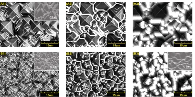
The alkali-based anisotropic wet chemical etching of (100)-oriented c-Si wa-fers results in the formation of regularly-shaped pyramids created by intersec-tions of {111} crystallographic planes [45]. These pyramids have the same shapes and facet orientations, but different sizes and randomly distributed locations on the wafer surface [see Fig. 2.2(A1, B1)].
Pyramidal textures were created on both surfaces of 280 µm thick n-type c-Si wafers using the alkaline 1.7 %-dilute KOH etching solution. This texturing process reduces the thickness of wafers to about 230 µm. Two different texturing procedures were applied. In the first solution, that we will name ”type A” the isopropyl alcohol (IPA) was used as an additive to the KOH solution, while in the second solution ”type B” an industrial surfactant (RenaTex) was added to the KOH solution.
First, the as-cut wafers were dipped for 3 minutes into a 22 %-NaOH solution
at 80◦C to remove damages related to the wire cutting of silicon ingots. Next, the
wafers were divided into two batches. One batch was textured using a type A solution for 30 minutes, while the second one was textured using a type B solution for 45 minutes. Type A solution gives larger pyramids featuring square basis of 10-15 µm as can be observed in Fig. 2.2(A1). On the other hand, type B solution leads to pyramids with smaller basis, reaching 4-5 µm [see Fig. 2.2(B1)].
In our work, we studied series of three samples of each type (A and B). For each type, there was a pyramidal sample without any additional surface post-treatment (A1 and B1), one sample after short additional surface post-post-treatment (A2 and B2), and one after long surface post-treatment (A3 and B3) (see Fig. 2.2). The objective of the post-treatment is to transform the sharp V-shaped surface morphology of the valley bottom into smoother U-shaped valleys by CP133
chemical solution at 14-22 ◦C. CP133 is a mixture of HF (50 % in H
2O), HNO3
(65 % in H2O), and CH3COOH (100 %) in 1:3:3 volume ratio proportions. The
short post-treatment of 70 and 40 seconds was used to produce samples A2 and B2, respectively. A 180 s long post-treatment was applied to obtain both A3 and B3 samples. Further details on texturation processes can be found in [43].
2.2
Radial junction solar cells
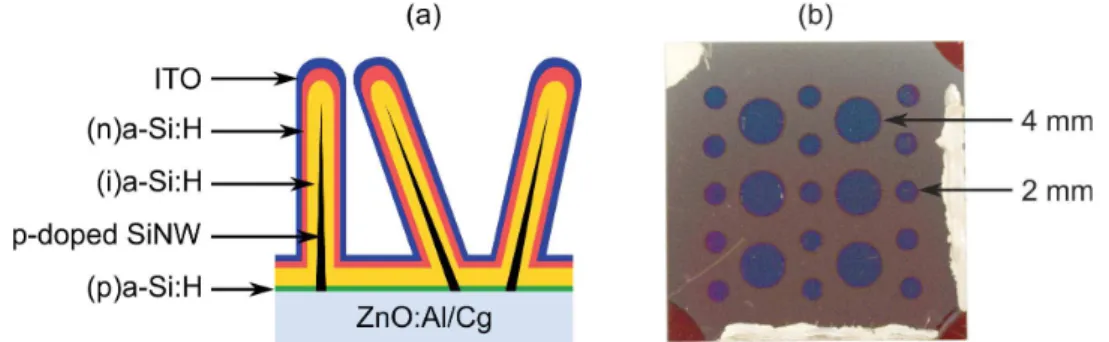
Radial junction solar cell fabrication consists of a PECVD deposition of in-trinsic and n-type a-Si:H layers over p-type silicon nanowire arrays grown by plasma-assisted VLS method, magnetron sputtering of ITO and creating silver contacts. Complete solar cell structure (without Ag contacts) is schematically drawn in Fig. 2.3(a) while an example of sample is shown in Fig. 2.3(b).
2.2. RADIAL JUNCTION SOLAR CELLS 15
10 um
(A1) (A2) (A3)
10 um
(B1) (B2)
10 um
(B3)
Figure 2.2 – Laser scanning confocal microscopy images of studied samples. (A1) type A without additional surface post-treatment, (A2) type A after short (70 s) surface post-treatment, (A3) type A after long (180 s) surface post-treatment, (B1) type B without surface treatment, (B2) type B after short (40 s) surface post-treatment, and (B3) type B after long (180 s) surface post-treatment. Inset figures show scanning electron microscopy (SEM) images of partially tilted samples A1, B1, and B3.
metal catalyst droplets is the most common bottom-up approach to synthesize SiNWs. In this process, the catalyst is heated above its eutectic temperature with Si, while gas precursors such as silane (SiH4) or silicon tetrachloride (SiCl4)
are preferentially adsorbed and decomposed at the surface of the liquid metal droplet. Upon dissolution into the droplet, Si atoms form a liquid eutectic al-loy with the catalyst material. Eventually, with the continuous flow of precursor gases, the alloy becomes supersaturated, overcomes the nucleation barrier and Si begins to precipitate at the liquid-solid interface in order to minimize the free energy of the system. As this process goes on, the alloy droplet gets displaced from the substrate leading to the growth of SiNWs [15].
A relatively high process temperature required in CVD (which is not com-patible with the use of low-cost substrates) can be reduced by using plasma-assisted VLS method which opens the way to the use of glass [46] and flexible substrates [47]. Furthermore, exploiting the plasma to dissociate gas precur-sors allows for the use of a wider range of metals which are not able to disso-ciate process gases by themselves (in contrast with Au) as mediators for SiNWs growth [48].
depo-16 CHAPTER 2. SAMPLE PREPARATION sition of thin films has the advantage, that a whole radial junction solar cell can be fabricated in just one-pump-down process and is compatible with industrial PECVD reactors.
Figure 2.3 – Radial junction solar cells built on silicon nanowire arrays. (a) Schematic drawing (the structure is not drawn to scale) and (b) photo of a sample with solar cells of 2 and 4 mm diameters.
A 100 nm thick absorber layer of (i)a-Si:H is deposited by PECVD over p-type
SiNWs. The deposition takes 60 min at 180◦C and the deposition conditions are:
10 sccm SiH4 flow rate, chamber pressure of 120 mTorr and RF power density of
20 mW/cm2[49]. Then, 1 sccm of phosphine (PH
31% diluted in H2) is introduced
into the reactor chamber as the dopant gas to deposit (n)a-Si:H layer to complete the PIN radial junction.
The radial junction solar cells are finalized by RF magnetron sputtering of ITO (In2O3: SnO2 = 9 : 1) at 180◦C to create the top contact [49]. A mask with circular
openings of 2 mm and 4 mm in diameter is used to define the solar cell areas [see Fig. 2.3(b)]. Finally, the tiny Ag dots are created in the middle of each solar cell to provide a good electrical contact for measuring probes.
2.2.1
Silicon nanowires grown for radial junction solar cells
Random silicon nanowire arrays are grown by plasma-assisted VLS method in a PECVD reactor. Tin was chosen as the metal mediator for SiNW growth [49],
since it is abundant, has low melting point (around 232◦C) and doesn’t introduce
undesirable deep defects in the band gap of Si [50] (in contrast with Au [51]) which increase the recombination rate of photogenerated carriers [52] and are detrimental for the carrier life-time and diffusion length.
The Sn layers with a nominal thickness of 2 nm were thermally evaporated on the 1 mm thick Corning glass substrate of inch by inch area covered by an aluminum doped ZnO (ZnO:Al) film of a nominal thickness of 2 µm. ZnO:Al
en-2.2. RADIAL JUNCTION SOLAR CELLS 17 vironment than other transparent TCOs such as ITO or fluorine-doped tin oxide
SnO2:F (FTO). It was deposited by RF magnetron sputtering at 180◦C.
Sn layers were exposed to H2 plasma for 2 min at 180◦C, to remove tin oxide
and form Sn droplets. The chamber pressure, the RF power density, and the
H2 flow rate were fixed at 600 mTorr, 25 mW/cm2 (nominal power of 5 W) and
100 sccm, respectively [49], to obtain well-separated metal droplets with narrow
size distributions. Then, the substrate temperature was increased to 400◦C and
after 10 min stabilization, 10 sccm of silane (SiH4) and 1 sccm of trimethylboron
(1% TMB diluted in H2) were introduced to initiate the growth of p-doped SiNWs
by plasma-assisted VLS method with 10 mW/cm2power density (nominal power
2 W) [16]. The conditions were kept constant during 10 min of SiNW growth resulting in 0.8-1 µm long nanowires with 30-50 nm diameter at their bases and less than 20 nm diameter at their tips. Figure 2.4 shows the crucial steps of the fabrication process.
Figure 2.4 – SEM images of (a) Sn deposited on the Corning glass substrate
cov-ered by ZnO:Al, (b) Sn droplets formation after 2 min of H2plasma treatment, and
(c) random silicon nanowires grown by plasma-assisted VLS method for 8 min-utes. Insets illustrate schematically the fabrication process steps [49].
19
3
Characterization methods
Outline
3.1 Total reflectance and transmittance measurements . . . 20 3.2 Standard and Mueller matrix ellipsometry . . . 20
3.2.1 Standard spectroscopic ellipsometry . . . 21
3.2.2 In-situ spectroscopic Mueller matrix ellipsometry . . . 22
20 CHAPTER 3. CHARACTERIZATION METHODS This chapter introduces methods which were used for characterization of studied samples. We have used mainly optical characterization methods as you can see below, since they are fast, non-destructive, and non-invasive and they can provide us a lot of valuable information not only about the sample optical properties but also about their structure. Moreover, some optical measurements can be carried out even in-situ in the reactor and allow us to monitor the sample during the fabrication process.
In Section 3.1 the spectroscopic measurement of total reflectance and trans-mittance is described. This section is followed by Section 3.2 on standard and Mueller matrix ellipsometry which is further divided into Section 3.2.1 devoted to the spectroscopic ellipsometry, Section 3.2.2 dealing with the in-situ Mueller matrix polarimetry, and Section 3.2.3 on angle-resolved Mueller matrix polarime-try.
3.1
Total reflectance and transmittance
measure-ments
PerkinElmer UV/Vis/NIR spectrophotometer Lambda 950 with a 150 mm in-tegrating sphere has been used to measure the sum of total reflectance and trans-mittance of the pyramidal textured wafers to assess the impact of the surface tex-ture on the light-trapping properties. The sum of the total specular and diffuse reflectance and transmittance of the sample corresponding to (R + T = 1 − A), where A is the absorptance, has been measured with the sample inside the inte-grating sphere in the spectral range from 250 to 1100 nm with an increment of 5 nm. All six samples with different surface treatments (see Fig. 2.2) were measured at the normal angle of incidence (AOI) with respect to the plane of the wafer. Sec-ond, both types of samples with no additional surface post-treatment (A1 and B1)
were also measured at oblique angles of incidence reaching values from 8◦to 60◦.
3.2
Standard and Mueller matrix ellipsometry
The advantage of using ellipsometric techniques such as standard spectro-scopic ellipsometry or Mueller matrix polarimetry is, that in contrast with the spectroscopy presented above in Section 3.1, the ellipsometric techniques mea-sure not only the change of amplitude but also the phase shift of polarized light after its interaction with a sample. This allow us to obtain more information about the studied sample. Following subsections describe measurement set-ups for dif-ferent types of ellipsometric techniques used for characterization of samples in this thesis. More details on the principles of ellipsometric measurements and the
3.2. STANDARD AND MUELLER MATRIX ELLIPSOMETRY 21 theory behind data analysis can be find in Section 4.3 of Chapter 4.
3.2.1
Standard spectroscopic ellipsometry
Ex-situ scanning spectroscopic phase modulated ellipsometer measurements (Uvisel 2, Horiba Scientific) of reference samples have been carried out to deter-mine optical functions of used materials. The Uvisel 2 with the 150 W Xenon light source was used to measure reference samples of of a-Si:H, a-SiC:H, (p)a-Si:H, (p++)a-(p)a-Si:H, ITO, Sn and ZnO:Al thin films on Corning glass substrates. The measurements have been performed in a wide spectral range of 230-2000 nm (0.6-5.4 eV) at the angle of incidence of 70◦.
Spectroscopic ellipsometry on pyramidal textures
Reduced reflectivity and high scattering of the pyramidal textured surface re-quire an increased light source intensity and specific measurement configurations for ellipsometric signal with a good signal to noise ratio [8].
Scanning spectroscopic phase modulated ellipsometer UVISEL 2 (Horiba Sci-entific) with a 150 W Xenon light source has been used to measure spectroscopic ellipsometry data of samples with pyramidal texture. This ellipsometer is equip-ped with a double monochromator system for the ultraviolet-visible (UV-VIS) range from 190 nm to 880 nm and twin photomultiplier tube detectors for the higher sensitivity and dynamic range. It has a near-infrared (NIR) extension, covering the spectral range up to 2100 nm, consisting of monochromator for NIR range (880-2100 nm) and InGaAs detector. This ellipsometer allows variable
an-gle spectroscopic ellipsometry measurements in the range from 35◦ to 90◦.
The lateral measurement geometry, which is based on aligning the pyramidal facets perpendicular to the plane of incidence, was used for measurements as described in Ref. [9]. An inclination stage has been used to align a sample to the required position in order to obtain specular reflection from the facets (for illustration see Fig. 3.1). First, the angle of incidence, set by a goniometer, was verified by a measurement of the reference flat wafer with a 22.1 nm layer of thermal oxide. Then, the textured sample was mounted on the inclination stage so that one straight edge of the quarter-wafer representing the [1¯10] direction was parallel to the plane of incidence. The computer controlled XYZ stage was used to adjust the spatial position of the sample. Then, we inclined the sample using the inclination stage to set the (1¯1¯1) facets of the pyramids to be in horizontal sample
plane. The ideal inclination angle of 54.74◦ (for ideal pyramids) corresponds to
the angle between a facet and a base of a pyramid defined by the geometry of
anisotropic wet-etching. The inclination angle of the stage was set to 55◦ and
22 CHAPTER 3. CHARACTERIZATION METHODS of the spot displayed by the vision system providing a real-time color image of the sample and exact measurement spot using the ellipsometer head.
Figure 3.1 – Measurement set-up for samples with pyramidal texture using the inclination stage of UVISEL 2 (Horiba Scientific) (a) and schematic representation of measurement geometry (b).
The accuracy of the sample adjustment was verified by comparison of the angle of incidence acquired from the ellipsometry measurement of the sample with the angle of incidence previously set by the goniometer. If the fitted AOI was not close to that one obtained for the reference sample, the adjusting of the inclination angle and sample height was repeated. All sample measurements were carried out with an integration time of 500 ms and an elliptic spot size of
2×0.7 mm (value corresponding to the angle of incidence of 70◦). The angles of
modulator and analyzer were set to 0◦ and +45◦, respectively.
3.2.2
In-situ spectroscopic Mueller matrix ellipsometry
We have used a Mueller matrix polarimeter (MM-16, Horiba Scientific) for a fast, non-destructive, large spot characterization of random silicon nanowire arrays during their growth. The MM-16 polarimeter has a liquid crystal based polarization state generator and analyzer allowing for measurements of all 15 elements of normalized Mueller matrices in the spectral range of 450 - 850 nm. Heads of MM-16 are fixed to the PECVD reactor windows (as shown in Fig. 3.2) to enable in-situ measurements during the deposition at the fixed angle of
inci-dence of 71.2◦. In-situ ellipsometric data has been measured every 1 min during
sample fabrication starting from Sn droplets formation by H2 plasma treatment
3.2. STANDARD AND MUELLER MATRIX ELLIPSOMETRY 23
Figure 3.2 – Mueller matrix polarimeter installed on the PECVD reactor Plasfil.
3.2.3
Angle-resolved Mueller matrix ellipsometry
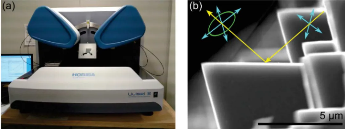
We have used angle-resolved Mueller matrix polarimeter (AR-MMP) with mi-croscope objective of high numerical aperture (NA = 0.95) to measure complete
Mueller matrices over the range of polar angles ϑ (0-60◦) and azimuthal angles φ
(0-360◦). The polarimeter enables measurements of all elements of Mueller
ma-trix in real and Fourier space at the same spot on the sample. A patented calibra-tion [53] of this device is based on the single value decomposicalibra-tion [54]. The spot size diameter can be adjusted from a few micrometers up to 50 µm using an iris aperture. A halogen lamp was used as the light source. For more information on the measurement setup see Ref. 55. We have used a fine pinhole aperture to select only the near normal angle of incidence from the objective back focal plane.
25
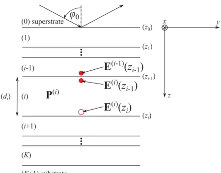
4
Theoretical background for optical modeling
Outline
4.1 Electromagnetic theory of light . . . 26
4.1.1 Maxwell equations in general medium . . . 26
4.1.2 Classification of material media . . . 27
4.1.3 Electromagnetic waves in non-absorbing medium . . . 30
4.1.4 Electromagnetic waves in absorbing medium . . . 32
4.2 Light propagation in thin film systems . . . 34
4.2.1 Yeh’s matrix formalism . . . 35
4.2.2 Optical intensity and power . . . 40
4.2.3 Reflection and transmission of light . . . 41
4.3 Principles of ellipsometric techniques . . . 44
4.3.1 Principles of spectroscopic ellipsometry . . . 45
4.3.2 Principles of Mueller matrix polarimetry . . . 46