HAL Id: hal-02271134
https://hal.archives-ouvertes.fr/hal-02271134
Submitted on 7 Jul 2020
HAL is a multi-disciplinary open access
archive for the deposit and dissemination of
sci-entific research documents, whether they are
pub-lished or not. The documents may come from
teaching and research institutions in France or
abroad, or from public or private research centers.
L’archive ouverte pluridisciplinaire HAL, est
destinée au dépôt et à la diffusion de documents
scientifiques de niveau recherche, publiés ou non,
émanant des établissements d’enseignement et de
recherche français ou étrangers, des laboratoires
publics ou privés.
17.2% efficiency CuIn 1– x Ga x Se 2 thin-film based
mini-module thanks to alternative architecture yielding
81% fill factor
Justine Lorthioir, Ludovic Arzel, Stéphane Ginestar, Lionel Assmann, Nicolas
Barreau
To cite this version:
Justine Lorthioir, Ludovic Arzel, Stéphane Ginestar, Lionel Assmann, Nicolas Barreau. 17.2%
effi-ciency CuIn 1– x Ga x Se 2 thin-film based mini-module thanks to alternative architecture yielding 81%
fill factor. EPJ Photovoltaics, EDP sciences, 2019, 10, pp.4. �10.1051/epjpv/2019003�. �hal-02271134�
R
EGULARA
RTICLE17.2% ef
ficiency CuIn
1
x
Ga
x
Se
2
thin-
film based mini-module
thanks to alternative architecture yielding 81%
fill factor
Justine Lorthioir1,*, Ludovic Arzel1, Stéphane Ginestar2, Lionel Assmann1, and Nicolas Barreau1
1
Institut des Matériaux Jean Rouxel (IMN)-UMR 6502, Université de Nantes, CNRS, 2 rue de la Houssinière, BP 32229, 44322 Nantes Cedex 3, France
2 Institut d’Électronique, de Télécommunications Rennes (IETR), UMR 6164, Université de Nantes, CNRS, 2 rue de la
Houssinière, BP 32229, 44322 Nantes Cedex 3, France
Received: 5 November 2018 / Received infinal form: 25 March 2019 / Accepted: 6 May 2019
Abstract. An alternative to conventional Cu(In,Ga)Se2module structure is proposed and experimentally
investigated. This alternative module structure, which consists in applying metallic buses to connect monolithically adjacent cells in series, is likely to offer the opportunity of minimizing both optical and electrical losses observed in conventional module structure compared to small area cells. The fabrication process of such alternative modules is presented. The performances achieved are discussed in comparison with a standard small-area-cell elaborated simultaneously. Despite slightly lower output voltage per cell, the alternative module structure demonstrates an efficiency of 17.2% (with 81% fill factor), against 16.4% (with 75% fill factor) for the standard cell. This promising result opens new routes to decrease the gap observed between small-area-cells and industrial modules.
Keywords: CIGSe / thin-film solar cells / alternative module structure
1 Introduction
Photovoltaic technology based on chalcopyrite Cu(In,Ga) (S,Se)2 (CIGSe) polycrystalline thin films has recently
achieved the outstanding efficiency level of 22.9% at the laboratory scale [1]. Nevertheless, there still exists a large gap between the performance of these small-area-cells and industrial modules. This gap originates, to a large extent, from the conventionally used monolithic cell interconnec-tion. Indeed, the industrial module structure implies three patterns (labeled P1, P2 and P3) for series connections [2]. Even when optimal, this conventional structure unavoid-ably leads to the losses listed below:
– the active area is decreased because of the interconnec-tion inactive zone (at least 10% of the total area); – the sheet resistance of the window layer, generally made
of ZnO:Al (AZO), has to be lowered down to about 5– 10V/sq to prevent increased series resistance. Increasing AZO thickness or free-carrier concentration induces additional photon absorption thus optical losses; – the expected ohmic contact between the window layer
and the Mo/MoSe2is generally associated with increased
series resistance.
In order to overcome these limitations, we investigated an alternative module structure, already proposed by the University of Uppsala two decades ago [3,4] and starts being industrially implemented by Solibro [5]. This modified structure relies on the use of metallic grids to monolithically connect adjacent cells.
In the present study, we show that such an approach indeed allows solving, at the laboratory scale, most of the limitations mentioned above.
2 Description of the alternative structure
As illustrated inFigure 1, the basic concept of the alternative module structure consists of using metallic buses to ensure the electrical connection between the Mo-rear contact of a cell N to the ZnO:Al topping electrode of the adjacent cell. This approach allows keeping the ZnO:Al window layer as thin and resistive as for small-scale cells design. Moreover, the electrical contact between the Mo and the metallic bus is expected to be stable and weakly resistive. Finally, this structure requires a single mechanical patterning, performed after the device stack is completed, and before metallic buses are deposited. In the present study, we used electron gun evaporated Ni/Al/Ni buses, as for the small area cells. The Mo-back contact has been patterned using photolithography as described in the following section. The resulting etched * e-mail:[email protected]
© J. Lorthioir et al., published byEDP Sciences, 2019
https://doi.org/10.1051/epjpv/2019003
EPJ
EPJ
PhotovoltaicsPhotovoltaicsAvailable online at:
www.epj-pv.org
This is an Open Access article distributed under the terms of the Creative Commons Attribution License (http://creativecommons.org/licenses/by/4.0), which permits unrestricted use, distribution, and reproduction in any medium, provided the original work is properly cited.
line width is about 150mm and complete in depth. A 2 mm-thick co-evaporated polycrystalline CIGSe thinfilm easily fills in the entire etched area.
3 Mo rear-contact patterning
As illustrated inFigure 1, the fabrication of the alternative module structurefirstly requires a specific patterning of the Mo layer. Photolithography was used to etch the back contact according to the required crenellated design. The different steps of this process are qualitatively illustrated in
Figure 2and the great lines of the experimental details are shortly described in the following.
Firstly, about 4mm of positive photoresist is applied by spin-coating onto the Mo layer, and baked for 3 minutes. The UV-light exposure through the photomask and the develop-ment durations were empirically adjusted. The
concentra-tion and pH of the etching soluconcentra-tion (K3[Fe(CN)6]) were also
optimized in order to achive sharp, well-defined Mo-edges, as shown by the SEM image presented inFigure 3.
One should notice that, as already mentioned, the approach followed here aimed at using the same shadow mask for the metallic buses as that used for the grids of small size solar cells; therefore, the etched line width (about 150mm) shown in Figure 3is far from the technological capabilities of the lithography actually employed in the field of silicon based microelectronics.
As a result, the series connection of adjacent cells is ensured by the metallic bus, contacting the Mo of the N 1 cell side and the AZO of the N cell side. For these first investigations, the alternative modules consisted of three connected cells (seeFig. 4).
4 Fabrication of devices
Both small size cells and alternative modules were fabricated on 1 mm-thick soda lime glass (SLG) coated with 400 nm-thick DC-sputtered Mo-layer. Independently (b)
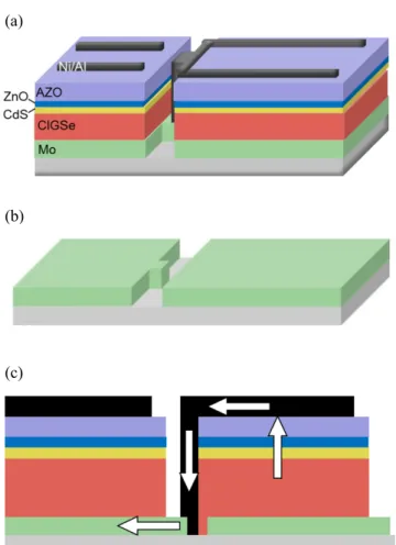
(a)
(c)
Fig. 1. Schematic representations (not to scale) of the alternative module with 3D view (a, b) and cross section (c). The top image shows the different layers: the metallic front contact (in black), the window ZnO/ZnO:Al (AZO) bilayer (in purple and blue), the CdS buffer layer (in yellow), the CIGSe absorber material (in red) and the Mo-back contact (in green). In addition, Figure 1b shows the patterned molybdenum layer. Figure 1cpresents interconnection layout between two adjacent cells, the electronsflow is illustrated by white arrows.
Fig. 2. Illustration of the photolithography process. Glass/ molybdenum substrates (1) are spin-coated with a positive photoresist (2). The resulting stack is exposed to UV light, throughout a laboratory-designed photomask (3). The soluble photoresist is washed away during the development (4). The unprotected molybdenum is etched with K3[Fe(CN)6] solution
(5). The unsoluble photoresist isfinally removed in aceton (6).
Fig. 3. Scanning electron microscopy image (top-view) of a patterned molybdenum-coated substrate.
of the targeted application (small size cell or module), CIGSe layers were co-evaporated following the conven-tional 3-stage process [6]. The mean gallium to group III (GGI) and copper to group III (CGI) ratios, determined by electron dispersive X-ray spectroscopy, are 0.3 and 0.9, respectively. After the CIGSe absorber layer is completed, a KF-post-deposition treatment was applied. A chemical bath deposited CdS layer was employed as n-type junction partner. The window layer consisted of conventional RF-sputtered ZnO/ZnO:Al bilayer; one should notice that the thickness and sheet resistance of the window is the same for cells and modules. For both targeted applications, Ni/Al/Ni grids were evaporated throughout a shadow mask. The resulting shadowing is expected being about 2% of 0.5 cm2cell area. No antireflection coating was applied to the devices.
To summarize, all of the fabrications steps were exactly the same for both types of devices (cells and modules); the only additional process steps for modules are the patterning of the Mo rear contact and mechanical P3 prior to metal grids deposition.
The performance of the resulting 0.5 cm2 cells and alternative modules (3 interconnected cells) were investi-gated from J(V) measurements (@ 25°C) under AM1.5G spectrum. A laboratory-made external quantum efficiency (EQE) setup was used to compare the performance of cells
and modules. Indeed, an additional interest of the alternative module architecture proposed is that each interconnected cell can be characterized individually by J(V) and EQE as illustrated in Figure 4. For individual cell J(V) measurement, only the investigated cell is illuminated and contacts are probed as for a small size cell. For the measurement of individual cell EQE, the incident photons are brought to the active area of the cell thanks to an opticalfiber, as illustrated inFigure 4.
5 Results
Figure 5plots representative J(V) curves of a cell (0.5 cm2) and an alternative module (3 cells connected in series), fabricated simultaneously. The corresponding photovolta-ic parameters are detailed inTable 1.
The most impressive photovoltaic parameter achieved by the alternative structure is undoubtedly thefill factor, which reached 81%. This high value results from very low series resistance (0.08V.cm2), which supports the relevance of applying metallic buses to interconnect adjacent cells.
As shown inFigure 6, both the EQE of the small size cell and of a representative cell in module are very similar, both showing about 31.3 mA/cm2.
In addition, those EQE suggest the absorbers have the same absorption threshold, hence similar optical band gap. This is important to mention because the output voltage of the module is 2.05 V (corresponding to 684 mV/ cell), whereas that of the solar cell is 702 mV. One should notice that the Vocof the cells constituting the modules
were also measured to be 685 ± 5 mV, therefore also lower than that of the small size cell. Those ∼20 mV/cell difference are still not fully understood and deserves caution. According to the representative results presented inTable 1, the extracted saturation current (J0) is four
decades lower for modules compared to cells. This suggests the effective holes concentration in CIGSe is higher for modules than for cells [7]. One could incriminate the CIGSe that grows directly onto soda-lime glass (where Fig. 4. Schematic of a typical 3-cell module. It shows Mo (green),
AZO (purple), metallic grids (black). The red arrows define the front and back contacts for both J(V) and EQE individual measurements. The whitefilled circle illustrates the illuminated area for EQE measurement.
Voltage
Fig. 5. J(V) characteristics measured under standard testing conditions, and adjusted to the Jsc deduced from the EQE
measurement (active area). The cell and the alternative module (3-cell) were fabricated simultaneously.
Table 1. Photovoltaic parameters of two representative devices fabricated simultaneously.
Cell Alternative module VOC/cell (mV) 702.0 684.0 JSC(mA/cm 2 ) 31.3* 31.2* FF (%) 75 81 Efficiency (%) 16.4 17.2
J0(A/cm2) 1.4E-8 8.3E-13
n 1.85 1.07 RS(V.cm2) 0.33 0.08 RSH(V.cm2) 453 316 VMP(mV) 570 1795 JMP(mA/cm2) 28.7 27.9 Pmax(mW) 8.2 25.1 *
the Mo has been etched) since this location undergoes a different substrate surface temperature and much higher sodium availability. Consequently, the structural, chemi-cal and electrichemi-cal properties of the polycrystalline layer synthesized directly on the bare SLG are probably very different to those of layers grown on SLG/Mo [8]. This hypothesis should assuredly be further explored in order to determine the origins of the lowered VOC per cell within
the module.
6 Summary
In the present study, we described alternative module architecture leading to high efficiency CIGSe photovoltaic devices. Thanks to the use of metallic buses connecting adjacent cells, it appears possible to overcome most of the limitations inherent to the conventional CIGSe module structure. As first attempt, we have fabricated a 3-cell module demonstrating a photovoltaic conversion efficiency of 17.2% (in-house measurement, active area), which over-performs the small size cell fabricated simultaneously. This result is very promising because there still exist many rooms for improvement. Beside this outstanding perfor-mance, the alternative architecture proposed offers many perspectives to better understand the operation of CIGSe
module since the design used allows characterizing each individual cell within a module.
This work is supported by the ADEME and Région Pays de la Loire. The authors would like to thank Fanch Guillou (from IMN) for his technical support and J. Kessler from B-Plan for fruitful discussions.
Author contribution statement
Lionel Assmann was in charge of back and top contacts deposition. Stephane Ginestar co-developped the process to pattern molybdenum back contacts. Justine Lorthioir organized the work through active layers deposition, co-developped patternings and wrote a largest part of the article. Ludovic Arzel co-supervised the work and made the simulations. Nicolas Barreau co-supervised the work and contributed to thefinal version of the paper.
References
1. Solar Frontier, Solar Frontier achieves world record thin-film solar cell efficiency of 22.9%, Solar Frontier Press Release, 17-Dec-2017 [Online], Available fromhttp://www.solar-frontier. com/eng/news/2017/1220_press.html
2. V. Probst et al., Advanced stacked elemental layer process for Cu(InGa)Se2thinfilm photovoltaic devices, Mater. Res. Soc.
Sym. Proc. 426, 165 (1996)
3. J. Kessler, J. Wennerberg, M. Bodegard, L. Stolt, Highly efficient Cu(In, Ga)Se2mini-modules, Sol. Energy Mater. Sol.
Cells 75, 35 (2003)
4. J. Wennerberg, J. Kessler, L. Stolt, Design of grided Cu(In, Ga)Se2thin-film PV modules, Sol. Energy Mater. Sol. Cells
67, 59 (2001)
5. E. Wallin, U. Malm, T. Jarmar, O. Lundberg, M. Edoff, L. Stolt, World-record Cu(In,Ga)Se2-based thin-film
sub-module with 17.4% efficiency, Prog. Photovol. 20, 851 (2012) 6. A.M. Gabor, J.R. Tuttle, D. Albin, M. Contreras, R. Noufi,
High efficiency CuInxGa1 xSe2 solar cells made from
(Inx,Ga1 x)2Se3precursorfilms, Appl. Phys. Lett. 65, 198 (1994)
7. T. Soga, Nanostructured Materials for Solar Energy Conver-sion (Elsevier, 2006)
8. J. Wennerberg, J. Kessler, L. Stolt, Degradation mechanisms of Cu(In,Ga)Se2-based thinfilm pv modules, in 16th European
Photovoltaic Solar Energy Conference, 2000, pp. 309–312
Cite this article as: Justine Lorthioir, Ludovic Arzel, Stéphane Ginestar, Lionel Assmann, Nicolas Barreau, 17.2% efficiency CuIn1 xGaxSe2thin-film based mini-module thanks to alternative architecture yielding 81% fill factor, EPJ Photovoltaics 10, 4
(2019)
l
Fig. 6. EQE of cell and alternative module based on CIGSe (without anti-reflective coating).