Optically-Enhanced Performance of Polymer Solar Cells with Low
Concentration of Gold Nanorods in the Anodic Buffer Layer
Alaa Y Mahmoud1,2, Jianming Zhang3, Dongling Ma3, Ricardo Izquierdo2, and Vo-Van Truong1
1Department of Physics, Concordia University, Montréal, Québec, Canada H4B 1R6. 2Département
d'informatique, Université du Québec à Montréal, Montréal, Québec, Canada H3C 3P8. 3Énergie,
Matériaux et Télécommunications, Institut National de la Recherche Scientifique (INRS) ,1650 Boulevard Lionel-Boulet, Varennes, Québec, Canada J3X 1S2
Abstract:
In this work, the effect of gold nanorods on the performance of poly(3-hexylthiophene-2,5-diyl):[6,6]-phenyl-C61-butyric-acid-methyl-ester bulk heterojunction solar cells was
investigated. Gold nanorods were introduced into the anodic buffer layer by simply blending them with the solution of poly(3,4-ethyl-enedioxythiophene):poly(styrenesulfonate). Even with a fairly low density of the nanorods, the resulting devices showed a remarkable 21.3% enhancement in the power conversion efficiency and a 13% enlargement in the short circuit current. By examining the absorbance profiles of active films made with different conditions, such enhancements can be related to the localized transverse and longitudinal plasmon resonance modes in the metallic nanoparticles. Gold nanorods helped as well in reducing the device series resistance by up to 36%, which also contributed to the global enhancement in the efficiency. Keywords: Gold nanorods, bulk heterojunction, organic solar cells, plasmonics
1. Introduction:
Organic solar cells (OSCs) have widely captured the attention of green energy researchers due to their interesting features such as low cost of fabrication, ease of manipulation, and lightweight [1]. The architecture of a bulk heterojunction (BHJ) solar cell has demonstrated its potential for enhancing the power conversion efficiency (PCE) by facilitating the excitons dissociation through an interpenetrating network between electron-donor and electron-acceptor materials [2]. Up to now, only 5% PCE has been achieved from a polymer:fullerene BHJ solar cell that comprises poly (3-hexylthiophene-2,5-diyl) (P3HT) as the polymer and [6,6]-phenyl-C61
-butyric-acid-methyl-ester (PCBM) as the fullerene derivative [3]. The absorption of the active layer (polymer:fullerene layer) is a very important factor for achieving a high photovoltaic (PV) performance [4]. The effective reported thickness for the active layer (~ 100-200 nm) [4-6] is too low for a complete absorption of the incident light within the absorption range of the active layer. Although enlarging the active layer thickness increases its light absorption, the low charge carrier mobilities [5, 6] reduce the efficiency of BHJ-OSC due to the increase in the charge carriers recombination and the device series resistance (Rs).
It has been reported that intensifying the electromagnetic (EM) field of the incident light via localized surface plasmon resonance (LSPR) in metallic nano-particles/structures (MNPs) helped in improving the absorption of the active layer with no need for increasing its thickness [4, 7]. LSPR occurs when the frequency of the electric field of the incident light resonates with the oscillations of MNPs conduction electrons. The excited MNPs thereby strongly absorb (near-field effect) and scatter (far-field effect) the incident light, producing an enhancement up to a factor of 100 [3], in the electric field surrounding them [8]. Previous studies showed that the PCE of BHJ-OSCs was improved considerably by MNPs incorporated into OSC layers either on top of indium tin oxide (ITO) [9-12], within poly(3,4-ethyl-enedioxythiophene):poly(styrenesulfonate) (PEDOT:PSS) [13- 15], within P3HT:PCBM [16], or with the back electrode [17].
Dunbar et al. [18] reported that the enhancement in the light absorption due to MNPs embedded in the OSCs layers is higher than that associated with placing them near front/back electrodes. This is due to their additional role in reducing the device series resistance. However, embedding MNPs in the active layer introduces quenching energy states for the excitons, which reduces the number of free charges carriers that are collected by electrodes [12, 16]. Hence, introducing MNPs in the anodic buffer layer (ABL) of OSCs would be a good approach. The effect of incorporating non-spherical MNPs into the ABL of BHJ-OSC has not been studied widely whereas all of the earlier studies were performed using relatively spherical particles [14-15]. The fact that the plasmonic absorption mode is a shape-dependent property [19], and the possibility of having higher fraction of the forward-scattered light using cylindrical particles rather than the spherical ones [20] motivate the use of gold nanorods (Au NRs) in the present work. Besides, the resonance peaks of Au NRs are situated around the absorption features of P3HT:PCBM.
In the current study, we report the influence of Au NRs on the performance of OSC by a direct blending of different amounts of Au NRs solutions with PEDOT:PSS solution. The contiguous contact between the ABL and the P3HT:PCBM layer makes it possible for the intensified electromagnetic field around the Au NRs to reach the P3HT:PCBM layer, thereby
improving its absorption of light. By investigating the absorbance profiles of several active films made with different conditions, we can relate the enhancement in the device performance to the transverse and longitudinal plasmonic modes of Au NRs.
2. Experimental methods:
Gold nanorods, Fig. 1, were synthesized following our previously reported method in reference [12]. The concentration of Au NRs in the aqueous solution was ~1.593×10¹² rods/ml. In
order to prepare the modified ABL with Au NRs, the NRs solution was mixed with the PEDOT:PSS (CLEVIOS™ P VP Al 4083) solution. The mixture was done by adding determined volume-percentages of the Au NRs solution (30, 15, 7.5%) to the PEDOT:PSS solution. The concentration of the PEDOT:PSS in the final mixture was intentionally kept constant by adding an additional volume of DI-water to the mixtures.
For OSC fabrication [12], the active layer solution was prepared inside a nitrogen glove-box by separately dissolving a 20 mg of P3HT (98% regioregularity, Rieke Metals) and a 16 mg of PCBM (>99.5%, Sigma-Aldrich) in 1 ml of 1, 2-dichlorobenzene. Equal volumes of P3HT and PCBM solutions were then mixed together and stirred overnight at room temperature. The molecular structures of P3HT and PCBM are presented in Fig. 2a. Patterned ITO-coated glass substrates were cleaned and treated with oxygen plasma before spin-coating ~ 30 nm film of PEDOT:PSS with/without Au NRs. Afterward, substrates were baked at 120 oC for 1 h before
spin-coating the active film P3HT:PCBM. A bilayer LiF/Al cathode was then thermally evaporated under pressure less than 10-6 torr. Finally, devices were post-annealed at 150oC for 30
min inside the glove box. The final configurations of a device with ABL made of Au NRs embedded in the PEDOT:PSS is shown in Fig. 2b. The resulting devices were characterized in air using a solar simulator (xenon lamp-Oriel instruments) that was equipped with AM 1.5G filter. The output intensity of the lamp was adjusted to 100 mW/cm2 using a silicon photodiode (LI-200
Pyranometer). The current-voltage (JV) measurements were carried out using a source-meter (Keithley 2400). The PV parameters: open circuit voltage (Voc), short circuit current (Jsc), fill factor (FF) and PCE were measured in devices with and without Au NRs, under the same experimental conditions.
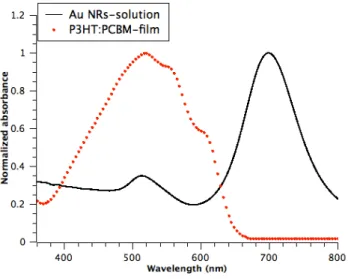
Fig. 3 compares the absorption spectrum for both P3HT:PCBM film and Au NRs solution. The black-line curve shows two plasmonic peaks, at 520 nm and 715 nm, for Au NRs, which resulted from the excitation of conduction electrons in the directions perpendicular (transverse mode) and parallel (longitudinal mode) to the rod long-axis, respectively [21]. The red-dot curve shows that the active layer absorption ranges from 370 nm to 650 nm, with an absorbance maximum around 518 nm and two shoulder peaks around 560 and 610 nm. It is clear that the resonance peaks for Au NRs are situated at or near the absorption maximum of the P3HT:PCBM. Besides, the longitudinal peak of Au NRs is close to the IR absorption edge of the active layer. Hence, the intensified electric field around the NRs would reach the active layer and increase its absorption near the plasmon peaks of the NRs, even though the total enhancement remains small near the IR wavelengths.
In order to picture the Au NRs density and orientation in the PEDOT:PSS layer, scanning electron microscopy (SEM), Fig. 4, was performed for the PEDOT:PSS:AuNRs spin-coated film. The white droplet-like structures indicate the Au NRs. From the uniformity of the PEDOT:PSS:Au NRs film, we can presume that the NRs did not aggregate after being mixed with the PEDOT:PSS [3]. Furthermore, the orientations of Au NRs within the PEDOT:PSS film were arbitrary, and their density was very low.
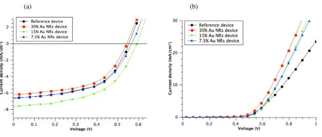
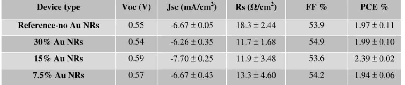
Fig. 5 shows the JV curves under illumination and in dark conditions for reference device along with devices containing Au NRs in the ABL, and table 1 summarizes the PV parameters. In our devices, the values of the PCE were generally low due to the devices exposure to the air at a certain point during evaporation and characterization processes. It can be seen from table 1 that the 7% and 15% Au NRs devices showed an increase in both Jsc and PCE. The optimal value for the enhancement was observed from the 15% Au NRs devices, which has ~ 2.38 × 10¹¹ rods/ml in
the ABL solution. For these devices, we observed a clear enhancement in the Jsc from 6.6 to 7.7 mA/cm2, which lead to 21.3% enhancement in the PCE. We found such enhancement quite
interesting considering the low density of the MNPs in the layer as compared to some reported studies in which the density of the particles was much higher [9, 11, 15]. The density of the NRs embedded in the ABL of our samples was estimated from the SEM as ~ 6 - 8 × 10⁸ rods/cm2.
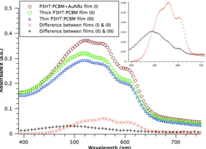
In order to determine whether the enhanced performance in our devices was indeed related to the plasmonic effect, we performed a comparative study between the absorbance of P3HT:PCBM film made with different conditions: pristine-thick, pristine-thin and thick P3HT:PCBM film with Au NRs. Fig.6 shows the absorbance profile of the resulting films: the brown-O curve corresponds to thick P3HT:PCBM:AuNRs (film I), the green-◊ curve corresponds to thick P3HT:PCBM (film II) and the blue-∆ curve corresponds to the thin P3HT:PCBM (film
III). The change in the P3HT:PCBM thicknesses was achieved by varying the spin-coater speed (RPM) from 1000 to 1500 for thick and thin films respectively.
As Fig. 6 shows, while the absorbance shapes of the three films are similar, the absorbance intensity varied and the highest one was associated with the Au NRs incorporated film. Due to the similarity in the absorbance shapes of those films, the multi-modes excitation-dependent for the film with Au NRs was not obvious. However, a clear plasmonic-related shape appeared by comparing the increase in the absorbance between films I and II (red-× curve) along with the one between films II and III (black + curve). Differences in the absorbance of films made at different conditions: (thick pristine film – thin pristine film) and (thick NR incorporated film - thick pristine film) gave the spectra shown in the inset of Fig. 6. The increase in the thickness of pristine P3HT:PCBM film shows a maximum around 480 nm. In contrast, Au NRs in the active layer produced a peak maximum around 560 nm and two shoulder peaks around 518 and 610 nm. From Fig. 3, the enhancement in the absorbance at 518 is related to the transverse mode of the NRs, while the enhancement at 560 and 610 could be linked to the tail of the longitudinal mode of the NRs. From these peaks and shoulders, we could conclude that both modes of Au NRs are active here. Hence the observed differences in the absorption shapes between films I, II and III would link the enhancement in the P3HT:PCBM absorption to the multi-modes excitation in Au NRs.
Figure 7a illustrates the external quantum efficiency (EQE) measurements for reference device along with the 15% Au NRs one. These measurements were carried out by varying the wavelengths of the incident light from 400 to 800 nm using a Newport 74000 monochromator. As the cut-off wavelength of our monochromator is around 400 nm, the EQE response was not measured below that wavelength. The power intensity of the incident light is calculated using a calibrated Si photodiode (Thorlabs FDS100). To show that the enhancement in the Jsc was dependent on the multi-modes excitation of Au NRs, we investigated in Fig. 7b the increase in the EQE via incorporating the 15% Au NRs in ABL solution. We found that the EQE was enhanced by up to 12-14% respectively around 520-640 nm, which are near to the transverse absorption mode of Au NRs and the tail of the longitudinal one, respectively. These enhancements in the EQE with incorporating Au NRs are higher than what is reported in the literature [4], showing the advantage of using Au NRs over other shapes of the nanoparticles. Although there was no large enhancement in the absorption profile of P3HT:PCBM:AuNRs near the IR region, a very small increase in the EQE was observed at this region, particularly at 670-700nm, which can be attributed to the longitudinal absorption mode of Au NRs. From this scenario, it is suggested that the photo-generation of excitons near the transverse and longitudinal absorption modes of Au
NRs was enhanced, which improved the total device efficiency. Our results are somewhat different from those obtained by Morfa et al. [9] who reported on enhancements in organic cells incorporating Ag nanoparticles. These authors observed a decrease in enhancement near 450 nm where Ag NPs absorb and an increase in the red part of the spectrum. Other groups however reported results similar to ours with the EQE curves for both reference and NPs devices having the same absorption ranges with a slight enhancement in the tail near the IR region [4, 11, 15].
In our devices, we would expect that the LSPR will enhance the local EM field near the MNPs, thereby intensifying the light that passed through the P3HT:PCBM layer. It is also possible that Au NRs helped trapping the incident light in the active layer via forward scattering mechanism. Thereby, the number of the photo-generated excitons inside the active layer would be increased [14, 16], which would then increase the number of the free charge carriers that were collected by electrodes. This would explain the enhancement in the devices Jsc, and the improvement in the PCE.
For denser Au NRs in the buffer layer, 30% devices, as listed in Table 1, the values for both Voc and Jsc were lower than the ones for the reference device. Since the thickness of ABL was ~ 30 nm, comparable to the long axis of the NRs, and the NRs orientations were arbitrary in that layer, a higher density of Au NRs would tend to have the rods located at the interface, touching the active layer. Therefore, we would expect that most of the photo-generated excitons near the ALB/P3HT:PCBM interface to be subjected to recombination processes. Hence, the number of free charge carriers that reached electrodes would be lowered, thus reducing both Voc and Jsc [7]. It is also possible that the larger density of NRs would prevent some light from reaching the active layer either by scattering or increased absorption in the NRs [15].
Table 1 also shows that by embedding Au NRs in the PEDOT:PSS layer, the devices series resistance (Rs) was reduced by up to 36%, which contributed to the total enhancement in the PCE. Au NRs in the PEDOT:PSS layer reduced the volume of the PEDOT:PSS, which lowered the value of Rs, and diminished the interfaces that holes had to travel through to reach the anode. This would facilitate the movement of holes toward the anode [16]. As Fig. 8 indicates, the reduction in the Rs could also be due to the work function of Au NRs, ~ -5.1 eV [16], that matches very well with both the polymer HOMO level and the PEDOT:PSS work function. With that scenario, Au NRs in the ABL would act as a hole-conductor interface, leading to a better extraction of the holes after being dissociated from the excitons. This would result in an increase in the number of free holes reaching the ITO-interface [16].
4. Conclusion:
An enhancement in the PCE of polymer solar cells by up to 22.3% has been achieved by fabricating OSCs that contained Au NRs embedded in the PEDOT:PSS layer. The investigation of the absorption profiles of devices with/without Au NRs revealed that the multi-modes excitations of LSPR in Au NRs, even with a low density of Au NRs, was able to intensify the light that reached the active layer, and increase the number of the free charge carriers, which enhanced the Jsc by up to 13%. In addition, the presence of Au NRs in the anodic buffer layer produced a significant reduction in the device series resistance by up to 36%, which lead to a better collection of the charge carriers. This reduction contributed to the total enhancement in the device performance. Higher densities of Au NRs in the PEDOT:PSS layer were however found to reduce the overall performance of OSCs. Such reduction in the PCE could be related to the surface recombination of charge carriers that limited their numbers reaching the electrodes, or the fact that a large part of the incident light was prevented from reaching the active layer for a potential generation of excitons.
Acknowledgements:
Alaa Mahmoud acknowledges with thanks King Abdul-Aziz University, Saudi Arabia, for the financial support, Drs. Zain Yamani and Ahmed Mounir for the support and helpful discussion, Dr. Muthukumaran Packirisamy and Menouer Saidani for their advices and generous technical help. This work was supported by the Natural Sciences and Engineering Research Council of Canada.
Figures and Captions
Fig. 1. A transmission-electron-microscopy (TEM) image of Au NRs. The average dimensions of the rod are 40 nm and 10 nm for the long and short axes, respectively.
(a) (b)
Fig. 2. (a) The molecular structures for the active layer materials P3HT and PCBM; (b) A schematic diagram for OSC devices showing the Au NRs incorporated in the PEDOT:PSS anodic-buffer layer.
Fig. 3. The absorption modes of a P3HT:PCBM film (red-dot curve) and an Au NRs colloidal solution (black-line curve).
Fig. 4. An SEM micrograph of PEDOT:PSS:AuNRs film made with 15% of Au NRs solution in the PEDOT:PSS
solution. The bar in the inset is 300nm.
(a) (b)
Fig. 5. The JV curves for reference device along with devices incorporating Au NRs (a) Under illumination
Fig. 6. A comparison between the absorption profiles of the P3HT:PCBM films made with three different
conditions: thick-pristine (green-◊), thin-pristine (blue -∆), and thick with AuNRs spin-coated on top of it (brown-O). The change in the P3HT:PCBM thicknesses was achieved by varying the spin-coater speed. The difference between the
absorbance of thick and thin films is presented by the black-+ curve, and the difference between the absorbance of pristine and Au NRs film is presented by the red-× one. The inset shows the absorbance of both black-+ and red-×
profiles alone.
(a) (b)
Fig. 7. (a) The EQE spectral response for reference device along with the 15% Au NRs one; (b) The increase in the EQE with 15% Au NRs device along with the absorbance of the Au NRs solution. The curve has been smoothed
Fig. 8. The energy band diagram of the used materials showing the good match of the Au NRs work-function
with the HOMO of the polymer (P3HTH) and the work-function of PEDOT:PSS.
Tables and Captions
Device type Voc (V) Jsc (mA/cm2) Rs (Ω/cm2) FF % PCE % Reference-no Au NRs 0.55 -6.67 ± 0.05 18.3 ± 2.44 53.9 1.97 ± 0.11
30% Au NRs 0.54 -6.26 ± 0.35 11.7 ± 1.68 54.9 1.99 ± 0.10 15% Au NRs 0.59 -7.70 ± 0.25 11.9 ± 3.48 53.6 2.39 ± 0.02 7.5% Au NRs 0.57 -6.67 ± 0.43 13.3 ± 4.60 54.2 1.94 ± 0.06
Table 1. The average value of the PV parameters for reference and Au NRs devices, and the corresponding standard deviation. Theses values are obtained from at least five devices made under the same conditions. Rs was
extracted from the slope of the JV characteristics in the dark condition at 0.8V.
References:
[1] A. Moliton, J-M. Nunzi, How to model the behaviour of organic photovoltaic cells, Polym. Int. 55
(2006) 583-600.
[2] C-S. Ho, E-L. Huang, W-C. Hsu, C-S. Lee, Y-N. Lai, W-H. Lai, Effects of annealing on polymer
solar cells with high polythiophene–fullerene concentrations, Jpn. J. Appl. Phys. 50 (2011) 04DK21.
[3] W. Ma, C. Yang, K. Lee, A. Heeger, Thermally stable efficient polymer solar cells with nanoscale
[4] J-L. Wu, F-C. Chen, Y-S. Hsiao, F-C. Chien, P. Chen, C-H. Kuo, M.H. Hung, C-S. Hsu, Surface plasmonic effects of metallic nanoparticles on the performance of polymer bulk heterojunction solar cells, ACS Pub. 5 (2011) 959-967.
[5] A. J. Moulé, J. B. Bonekamp, K. Meerhol, The effect of active layer thickness and composition on
the performance of bulk-heterojunction solar cells, J. App. Phys. 100 (2006) 094503.
[6] J. Peet, I. Wen, P. Byrne, S. Rodman, K. Forberich, Y. Shao, N. Drolet, R. Gaudiana, G. Dennler,
D. Waller, Bulk heterojunction solar cells with thick active layer and high fill factors enabled by a bithiophene-co-thiazolothiazole push-pull copolymer, App. Phys. Lett. 98 (2011) 043301.
[7] W-J. Yoon, K-Y. Jung, J. Liu, T. Duraisamy, R. Revur, F-L. Teixeira, S. Sengupta, P-R. Berger,
Plasmon-enhanced optical absorption and photocurrent in organic bulk heterojunction photovoltaic devices using self-assembled layer of silver nanoparitcles, Sol. Energ. Mat. Sol. C. 94 (2010) 128-132.
[8] M. Pelton, J. Aizpurua, G. Bryant, Metal-nanoparticle plasmonics, Laser Photonics Rev. 2 (2008)
136–159.
[9] A. J. Morfa, K.L. Rowlen, Plasmon-enhanced solar energy conversion in organic bulk
heterojunction photovoltaics, App. Phys. Lett. 92 (2008) 013504.
[10] D. Duche, P. Torchio, L. Escoubas, F. Monestier, J-J. Simon, Improving light absorption in
organic solar cells by plasmonic contribution, Sol. Energ. Mater. Sol. C. 93 (2009) 1377-1382.
[11] J-H. Lee, J-H. Park, J-S. Kim, D-Y. Lee, K. Cho, High eficiency polymer solar cells with wet deposited plasmonic gold nanodots, Org. Electronics. 10 (2009) 416-420.
[12] A. Y. Mahmoud, J. Zhang, J. K. Baral, R. Izquierdo, D. Ma, M. Packirisamy, V.-V. Truong, Low
density of gold nanorods in the anodic layer of organic solar cells, Proc. SPIE 8007 (2011) 80071V.
[13] L. Qiao, D. Wang, L. Zuo, Y. Ye, J. Qian, H. Chen, A She, Localized surface plasmon resonance
enhanced organic solar cell with gold nanospheres, App. Energ. 88 (2011) 848–852.
[14] S-S. Kim, S-I. Na, J. Jo, D-Y. Kim, Y-C. Nah, Plasmon enhanced performance of organic solar
cells using electrodeposited Ag nanoparticles, App. Phys. Lett. 93 (2008) 073307.
[15] F-C. Chen, J-L. Wu, C-L. Lee, Y. Hong, C-H. Kuo, M. H. Huang, Plasmonic-enhanced polymer
photovoltaic devices incorporating solution-processable metal nanoparticles, App. Phys. Lett. 95 (2009) 013305.
[16] D. H. Wang, D. Y. Kim, K. W. Choi, J. H. Seo, S. H. Im, J. H. Park, O. Park, A. J. Heeger, Enhancement of donor-acceptor polymer bulk heterojunction solar cell power conversion efficiencies by addition of Au nanoparticles. Angew. Chem. Int. Ed. 50 (2011) 5519-5523.
[17] X. Chen, C. Zhao, L. Rothberg, M-K. Ng, Plasmon enhancement of bulk heterojunction organic
photovoltaic devices by electrode modification, App. Phys. lett. 93 (2008) 123302.
[18] R. B. Dunbar, T. Pfadler, L. Schmidt-Mende, Highly absorbing solar cells-a survey of plasmonic
nanostructures, Opt. Express 20 (2012) 177-189.
[19] P. K. Jain, S. Eustis, M. A. El-Sayed, Plasmon coupling in nanorod assemblies: Optical absorption, discrete dipole approximation simulation, and exciton-coupling model, J. Phys. Chem. B. 110 (2006) 18243-18253.
[20] K. R. Catchpole, A. Polman, Design principles for particle plasmon enhanced solar cells, App. Phys. Lett. 93 (2008) 191113.
[21] T-K. Sau, C-J. Murphy, Seeded high yield synthesis of short Au nanorods in aqueous solution,