To cite this version : Benchikhi, Mohamed and Ouatib, Rachida El
and Guillemet-Fritsch, Sophie and Chane-Ching, Jean-Yves and
Demai, Jean-Jacques and Er-Rakho, Lahcen and Durand, Bernard
Synthesis of CuInS2 nanometric powder by reaction in molten KSCN.
(2014) Materials Letters, vol. 136. pp. 431-434. ISSN 0167-577X
To link to this article : doi:
10.1016/j.matlet.2014.08.101
URL :
http://dx.doi.org/10.1016/j.matlet.2014.08.101
O
pen
A
rchive
T
OULOUSE
A
rchive
O
uverte (
OATAO
)
OATAO is an open access repository that collects the work of Toulouse researchers and
makes it freely available over the web where possible.
This is an author-deposited version published in :
http://oatao.univ-toulouse.fr/
Eprints ID : 14122
Any correspondance concerning this service should be sent to the repository
administrator:
staff-oatao@listes-diff.inp-toulouse.fr
Synthesis of CuInS
2
nanometric powder by reaction in molten KSCN
Mohamed Benchikhi
a,b, Rachida El Ouatib
a, Sophie Guillemet-Fritsch
b,
Jean Yves Chane-Ching
b, Jean Jacques Demai
b, Lahcen Er-Rakho
a, Bernard Durand
b,naLaboratoire de Physico-Chimie des Matériaux Inorganiques, Université Hassan II Casablanca, Marocco bInstitut Carnot CIRIMAT, CNRS Université de Toulouse, 118 route de Narbonne, 31062 Toulouse Cedex 9, France
Keywords: Chalcogenide Semiconductor Molten salt Nanoparticles
a b s t r a c t
CuInS2was synthesized, with a yield of 70% by reaction in molten KSCN at 400 1C of CuCl2and InCl3
with a ratio KSCN/Cu ¼ 15. The homogeneous powder obtained is constituted of nano-sized grains (70–100 nm), with a specific surface area of 6 m2/g and a band gap Eg of 1.5 eV.
1. Introduction
An intensive research was carried out on ternary I–III–VI and
quaternary I–II–IV–VI2 chalcogenides of chalcopyrite type
struc-ture, characterized by active conductive properties in photovoltaic
conversion [1–5]. Among them, the ternary CuInS2 exhibits a
specific interest because of its gap Eg (1.5 eV) very close to the
theoretical optimum for solar energy conversion[6,7]. The
elec-tron transitions being direct in this sulfide with a high absorption
coefficient (105cm 1
), thin films (a few micrometers)[8,9]can be
involved for the building of solar devices, minimizing the cost of solar material.
Numerous methods have been developed to prepare this
sulfide. The physical ones, laser removal[10], sputtering[11,12],
evaporation[13], co-evaporation [14,15]and electrodeposition
[6,16,17]are generally expensive and lead to thin layers with micro-sized particles. Among the chemical ones, the solvother-mal and organometallic routes are mainly used. They generally lead to homogeneous powders with grain sizes in the range 3–100 nm. The size of particles is dependent upon the nature of the solvents, precursors and temperature of pyrolysis of the
precursors[18,19].
In molten state at temperature in the range of 100–800 1C, the salts are ionic liquids where chemical reactions can be carried out
as in usual solvents[20–22]. Molten salts may be used as flux. For
instance, MgFe2O4 can be obtained at temperature as low as
900 1C by reaction of MgO and Fe2O3in the presence of molten
Li2SO4–K2SO4eutectic (Eq.(1)), whereas the same transformation
in solid state requires a temperature overcoming 1200 1C:
MgOðsÞþ Fe2O3ðsÞ ⟹
Li2SO4 K2SO4ðlÞ
MgFe2O4ðsÞ ð1Þ
Yet the versatility of the process is considerably improved when molten salts are directly involved in the chemical reaction. For the preparation of oxides, two types of transformations have been
often considered[23,24]:
$
Reactions between a mixed alkaline oxide and a molten divalentmetal chloride likely to lead to the formation of MgFe2O4 at
temperature as low as 600 1C according to the following equation:.
2LiFeO2(s)þ K2MgCl4(l)-MgFe2O4(s) þ4(Li/K)Cl(l) (2)
$
Reactions between a transition metal salt and a molten alkalinitrate as illustrated by Eq.(3)for the preparation of zirconia can
be obtained at temperature as low as 450 1C:
ZrOCl2(s) þ(K,Na)NO3(l)-ZrO2(s) þNO2(g) þ0.5Cl2(g)
þ (K,Na)Cl(l) (3)
Previous studies on the behavior of transition metal cations in molten potassium thiocyanate demonstrated the possibility to
synthesize sulfides[25]. Only a few papers consider the properties
of the powders obtained. Geantet et al.[26] presented the
hydro-treating properties of a MoS2 catalyst prepared from thiocyanate
melts. Benchikhi et al.[5]proposed a process route to the fabrication
of quaternary chalcogenides by reaction in molten KSCN at 400 1C. http://dx.doi.org/10.1016/j.matlet.2014.08.101
n
Corresponding author.
The main advantage of synthesis by reaction in molten salts lies in the chemical homogeneity of the powders obtained and on the control of the particle size.
The present paper describes the synthesis of nano-sized
homo-geneous powder of CuInS2by reaction of CuCl2and InCl3with molten
KSCN at 400 1C. The characteristics of the powder obtained are given.
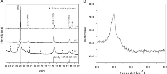
Fig. 1. Structural characterization: (A) RXD patterns of CuInS2prepared at 300 1C (a) 400 1C (b) and 500 1C (c). (B) Raman spectrum of CuInS2prepared at 400 1C.
2. Experimental
CuInS2 was prepared from the following precursors: InCl3
(Aldrich) and CuCl2% 2H2O (Sigma). KSCN (Prolabo) was used both
as solvent and sulfurizating agent. The equimolar mixture of chlorides was added to KSCN in the molar ratio SCN/Cu¼15. The thermal treatment was performed under nitrogen flow in a vertical furnace at temperatures comprised between 300 and 500 1C for 24 h. The heating and the cooling rates were stated at 2 1C/min. The reaction yield reached 70%.
After cooling and solidification of the molten medium, the sulfides were extracted from the excess of salt by washing with water and drying. The black powders obtained were characterized
by XRD (Brucker AXS D4,
λ
CuKα
¼ 1.5418 nm), SEM (JEOL JSM6400), TEM (JEOL 2010), specific surface area measurement (BET) (Micrometrics Flowsorb II 2300), Raman (Jobin Yvon Labram HR 800) and UV–visible (UV-1601) spectroscopies.
3. Results and discussion
Structural characterization: For the powder prepared at 300 1C,
the XRD pattern (Fig. 1Aa) identifies a main phase chalcopyrite
CuInS2 (JCPDS 047-1372) besides minor phases which could be
metallic sulfides (In2S3, CuSx). The peaks of the minor phases are
no longer present in the patterns of the sulfides prepared at 400 (Fig. 1Ab) and 500 1C (Fig. 1Ac). The decrease of the full width at half maximum of the XRD peaks of the chalcogenide phase, as the synthesis temperature was raised from 300 to 500 1C, is attributed to the increase of primary crystallite sizes.
Raman investigation was performed to fully characterize the
samples. The spectrum of the powder prepared at 400 1C (Fig. 1B)
exhibits a main peak close to 295 cm 1 and a shoulder close
to 314–315 cm 1. These signals are consistent with the vibration
involving the motion of sulfur atoms of ternary chalcogenides,
principal mode A1 and secondary mode B2/E observed in the
chalcopyrite phase[27–30].
Mechanism of formation: The formation of CuInS2 occurs in
three steps[21,22,31]: first the thermal decomposition of KSCN
starting at 275 1C with S and S2 formation via reactions (4) and
(5), then the reduction of Cu2 þby SCN involving the formation of
a complex of transition via reaction (6) and lastly the formation of the chalcopyrite phase via reaction (7):
SCN ¼ CN þ S; ð4Þ 2CN þ S ¼ S2 þ ðCNÞ2; ð5Þ Cu2 þþ 2SCN ¼ Cu SCN ð Þ2n ¼ Cuþþ12ðCNÞ2þ SCN þ S ð6Þ Cuþþ In3 þþ 2S2 ¼ CuInS 2: ð7Þ
Morphological characterization: SEM observation of the samples
synthesized at 400 and 500 1C (Fig. 2a and b) shows largely
agglomerated particles with a poly-disperse size distribution. The size of agglomerates increases with increasing temperature
synthesis. The agglomerates (Fig. 2c and d) are constituted of
nano-sized primary crystallites with more or less elongated shape.
It is noticed (Table 1) that the mean sizes of particles calculated
from the specific surface area values, assuming mono-disperse spherical particles, are higher than the sizes observed on TEM micrographs. This difference is attributed to the agglomeration of particles.
Measurement of the band gap Eg: The energetic value of the band gap of a semiconductor determines the part of the solar spectrum that could be theoretically absorbed by the material. From the UV–visible absorption spectrum of the sulfide powder
prepared at 400 1C (Fig. 3), the band gap Eg of the semiconductor
with a direct transition is determined using the following equation [32]:
ð
α
hν
Þ ¼ Aðhν
EgÞ1=2 ð8ÞWhere
α
is the absorption coefficient (cm 1), hν
the energy of theincident photons (eV) and A a constant. The Eg value of 1.51 eV is determined by the intersection of the linear part of the curve
(
α
hν
)2versus hν
(insetFig. 3). This value is in agreement with theones of the literature, 1.55 eV for single crystals[33]and 1.44 eV
for CuInS2films deposited by CVD[34]or 1.50–1.52 eV for samples
prepared by pulverization of indium and copper followed by a
sulfuration step[35].
4. Conclusion
The chalcopyrite phase CuInS2was prepared by the reaction in
a molten salt. The powder obtained in KSCN medium at 400 1C for 24 h with the ratio KSCN/Cu ¼15 is constituted of crystallites with sizes in the range 70–100 nm and exhibits a specific surface area
close to 6 m2/g and a gap Eg close to 1.5 eV suitable for application
in the photovoltaic conversion of solar energy.
Acknowledgments
This work was supported by two French-Moroccan projects: Volubilis Partenariat Hubert Curien (PHC no. MA 09 205) and Projet de Recherches Convention Internationale du CNRS (CNRS-CNRST no. w22572).
Table 1
Morphological characteristics. (The mean size of particles is calculated from the specific surface area according to the formula D¼6/dS, D is the mean diameter, d the density and S the specific surface area.).
Temperature (1C)
Specific surface area (m2/g)
Grain size (MET) (nm)
Mean grain size (nm) 400 5.9 70–100 200 500 3.5 130–150 340 400 600 800 1000 1200 1400 2.50 2.25 2.00 1.75 1.50 1.25 ( α h ν ) 2 (a . u ) hν (eV) Eg =1.51eV 1.00 1.0 0.8 0.6 0.4 Absorbance (a.u) wave length (nm) 0.2
References
[1]Nadenau V, Hariskos D, Schock HW, Kreijci M, Haug F, Tiwari A, et al. Appl Phys 1999;85:534–42.
[2]Aggour M, Störkel U, Murrell C, Campbell SA, Jungblut H, Hoffmann, et al. Thin Solid Films 2002;403–404:57–61.
[3]Hironori K. Thin Solid Films 2005;480–481(1):426–32.
[4]Hironori K, Kotoe S, Tsukasa W. Sol Energ Mater Sol Cells 2001;65(1–4):141–7. [5]Benchikhi M, Zaberca O, El Ouatib R, Durand B, Oftinger F, Balocchi A, et al.
Mater Lett 2012;68:340–3.
[6]Scragg JJ, Dale PJ, Peter LM. Thin Solid Films 2009;517:2481–4. [7]Arici E, Sariciftci NS, Meissner D. Adv Funct Mater 2003;13:165–71. [8]Pathan HM, Lokhande CD. Appl Surf Sci 2004;11:239–54.
[9]Katagiri H, Sasaguchi N, Hando S, Hoshino S, Ohashi J, Yokota T. Sol Energy Mater Sol Cells 1997;49:407–14.
[10]Shuaibov AK, Churchman MP, Dashchenko AI. Tech Phys Lett 2003;29:408–10. [11]Jaffe JE, Zunger A. Phys Rev B 1983;28:5822–47.
[12]Seol JS, Lee SY, Lee JC, Nam HD, Kim KH. Sol Energy Mater Sol Cells 2003;75:155–62.
[13]Kazmerski LL, Sanborn GA. J Appl Phys 1977;48:3178–80.
[14]Scheer R, Walter T, Schock HW, Fearheiley ML, Lewerenz HJ. Appl Phys Lett 1993;63:3294–6.
[15]Tanaka T, Kawasaki D, Nishio M, Guo Q, Ogawa H. Phys Status Solidi C 2006;3:2844–7.
[16]Herrero J, Ortoga J. Sol Energy Mater 1990;20:53–65. [17]Hodes G, Cahen D. Sol Cells 1986;16:245–54.
[18]Nyari T, Barvinschi P, Baies R, Vlazan P, Barvinschi F, Dékany I. J Cryst Growth 2005;275:2383–7.
[19]Gardner JS, Shurdha E, Wang C, Lau LD, Rodriguez RG, Pak JJ. J Nanopart Res 2008;10:633–41.
[20] Charlot G, Tremillon B. les réactions dans les solvants et les sels fondus. Gauthier-Villars; Paris; 1963; 486 (Chapter XV).
[21]Eluard A, Tremillon B. J Electroanal Chem 1967;13:208–12. [22] Collado S, Laca A, Diaz M. J Hazard Mater 2010;177:183–9.
[23] Durand B. Ceramic Powders. In: Vincenzini P, editor. Amsterdam: Elsevier Science. Publishing. Co.; 1983. p. 413–20.
[24] Durand B, Roubin M. Mater Sci Forum 1991;73–75:663–8. [25] Kerridge DH, Walker SJ. Inorg Nucl Chem 1977;39:1579–85.
[26] Geantet C, Kerridge DH, Decamp T, Durand B, Breysse M. Mater Sci Forum 1991;73–75:693–8.
[27] Guha P, Das D, Maity A-B, Ganguli D, Chaudhuri S. Sol Energy Mater Sol Cells 2003;80:115–30.
[28] Kondo K, Nakamura S, Sato K. J Appl Phys 1998;37:5728–36.
[29] Das K, Panda S-K, Gorai S, Mishra P, Chaudhuri S. Mater Res Bull 2008;43:2742–50.
[30] Palm J, Jost S, Hock R, Probst V. Thin Solid Films 2007;515:5913–6. [31]Tian Y, He Y, Zhu Y-F. Chem. Let 2003;32:768–9.
[32] Gungor T, Tolunay HJ. Non-Cryst Solids 2001;282:197–202.
[33] Shay JL, Wernick JH. Ternary chalcopyrite semiconductors: growth, electronic properties and applications. Oxford New York: Pergamon Press; 1975. [34] Henderson DO, Mu R, Ueda A, Wu MH, Gordon EM, Tung YS, et al. Mater Des
2001;22:585–9.
[35] Klaer J, Bruns J, Henninger R, Siemer K, Klenk R, Ellmer K, et al. Semicond Sci Technol TI 1998;13:1456–8.