Science Arts & Métiers (SAM)
is an open access repository that collects the work of Arts et Métiers Institute of
Technology researchers and makes it freely available over the web where possible.
This is an author-deposited version published in: https://sam.ensam.eu Handle ID: .http://hdl.handle.net/10985/10565
To cite this version :
Emmanuel BROUSSEAU, Benoît ARNAL, Stéphane THIERY, Eric NYIRI, Olivier GIBARU - A simple and generic CAD/CAM approach for AFM probe-based machining - In: 11th International Conference and Exhibition on Laser Metrology, Machine Tool, CMM and Robotic Performance, LAMDAMAP 2015, Royaume-Uni, 2015-03-17 - 11th International Conference and Exhibition on Laser Metrology, Machine Tool, CMM and Robotic Performance, LAMDAMAP 2015 - 2015
Any correspondence concerning this service should be sent to the repository Administrator : [email protected]
Laser Metrology and Machine Performance XI
A simple and generic CAD/CAM approach for
AFM probe-based machining
E. Brousseau
1*, B. Arnal
2, S. Thiery
2, E. Nyiri
2, O. Gibaru
21
Cardiff School of Engineering, Cardiff University, Cardiff, UK
2
LSIS, Arts et Metiers ParisTech, Lille, France
*
Corresponding author: [email protected]
Abstract
Atomic Force Microscopy (AFM) probe-based machining allows surface structuring at the nano-scale via the mechanical modification of material. This results from the direct contact between the tip of an AFM probe and the surface of a sample.
Given that AFM instruments are primarily developed for obtaining high-resolution topography information of inspected specimen, raster scanning typically defines the trajectory followed by the tip of an AFM probe. Although most AFM manufacturers provide software modules to perform user-defined tip displacement operations, such additional solutions can be limited with respect to 1) the range of tip motions that can be designed, 2) the level of automation when defining tip displacement strategies and 3) the portability for easily transferring trajectories data between different AFM instruments. In this context, this research presents a feasibility study, which aims to demonstrate the applicability of a simple and generic CAD/CAM approach when implementing AFM probe-based nano-machining for producing two-dimensional (2D) features with a commercial AFM instrument.
1
Introduction
A few years after the invention of the Atomic Force Microscope (AFM) as a device for imaging the surface topography of specimens at the nano-scale [1], researchers also began to use AFM instruments as platforms for performing a variety of nano fabrication tasks [2-4]. One of this fabrication techniques, which
Laser Metrology and Machine Performance XI
started being investigated in the early nineties [5-7], focusses on implementing machining operations with the tip of an AFM probe. This process enables the structuring of surfaces at the nano-scale by relying on the mechanical modification of material caused by the direct contact between the AFM probe tip and the sample surface. The AFM probe-based mechanical machining process has a number of attractive characteristics such as being relatively simple, low-cost to implement, able to produce complex three dimensional (3D) features and applicable to machine a wide range of engineering materials such as metals, semiconductors and polymers [8].
When using a commercial AFM instrument, raster scan is the typical path generation strategy implemented to define the trajectory followed by the tip of the AFM probe. This is due to the fact that standard AFM devices are primarily developed for the purpose of imaging the surface topography of a specimen. Although software modules are also provided by most AFM manufacturers to perform user-defined tip displacement operations, such solutions are limited and only enables fairly basic operations when implementing the AFM probe-based machining process. In particular, it is difficult for users to design a wide range of tip cutting trajectories with a high level of automation and also to transfer easily such trajectories data between different AFM instruments. As a result, in order to conduct particular AFM probe-based nano fabrication operations for a given system, customised procedures and computer routines often have to be implemented to enable the realisation of a large variety of tip trajectories. In the last fifteen years, the development of such customised solutions has been presented in a number of studies, which include the work of Horkas et al. [9], Lekki et al. [10], Klehn and Kunze [11], Cruchon-Dupeyrat et al. [12] and Xu et al. [13].
However, a common drawback of these reported approaches is that they do not propose a solution where the generation of the tip cutting trajectories can be achieved in a fully automated manner while, at the same time, enabling the design and path planning steps to be conducted without purposely-built software programmes. Thus, in order to broaden the application areas of future AFM tip-based nano machining studies, it would be advantageous to develop automated, portable and flexible solutions that could enable 1) the path of AFM tips to be defined via widespread design software tools and 2) the implementation of such tip trajectories to be conducted on a broad range of AFM instruments. The most promising approach for enabling such an increased flexibility and automation of the design and AFM-based fabrication tasks is that reported by Johannes et al., although, in the case of these authors, it was implemented for AFM probe-based anodisation operations [14, 15]. In particular, Johannes and co-workers developed a nano-scale design environment that incorporated conventional CAD and CAM software solutions. The interesting aspect of this work is that the G-code file format was utilised to communicate the tip trajectories to an AFM controller. G-code is a widely used computer numerical control (CNC) programming language and thus, it is implemented by commonly found CAM software.
Laser Metrology and Machine Performance XI
Thus, for the purpose of automating AFM probe-based nano machining tasks, it appears natural to reuse such an approach. This is due to the maturity of existing CAD/CAM solutions which, for conventional cutting processes, enable the seamless integration of the 3D modelling and the tool path planning steps. Therefore, the purpose of the research presented in this paper is to follow the method put forward by Johannes and co-workers in the context of nano machining operations rather than anodisation lithography. In particular, the objective of this study is to demonstrate the applicability of a simple and generic CAD/CAM approach when implementing AFM probe-based nano-machining for producing two-dimensional (2D) features with a commercial AFM instrument.
2
CAD/CAM approach utilised
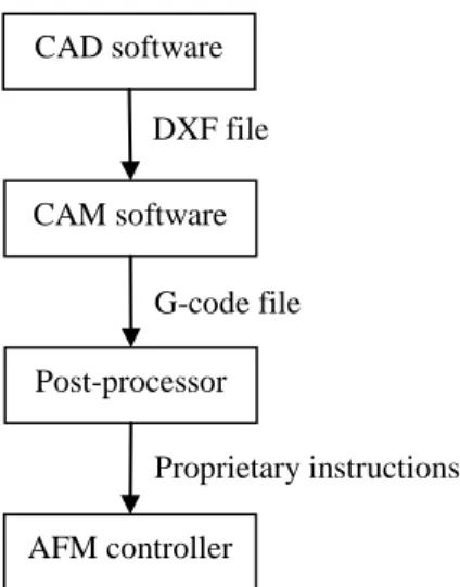
Fig. 1 illustrates the CAD/CAM approach followed in this study. Two different freely available software were used to implement the CAD and CAM stages of the process. These were “LibreCAD” and “DXF2GCODE”, respectively. A post-processor was developed to translate G-code data into instructions understandable by the AFM controller. This was achieved using C++ libraries provided by the AFM manufacturer. For this feasibility study, the post-processor was implemented to interpret four different type of G-code instructions only. These were “G0” for tip displacements without machining, “G1” for machining linear interpolations and “G2” and “G3” for machining circular interpolations clockwise and anti-clockwise, respectively.
Figure 1: CAD/CAM approach adopted
CAD software CAM software Post-processor G-code file DXF file AFM controller Proprietary instructionsLaser Metrology and Machine Performance XI
3
CAD/CAM demonstration
The AFM instrument utilised in this feasibility study was the XE-100 model from Park Systems. The probe employed to perform the machining experiments was a DNISP model from Bruker. This probe had a nominal normal spring constant of 221 N/m with a nominal tip radius of 40 nm as specified by the manufacturer. The workpiece processed was a single crystal copper sample 12 mm in diameter and 8 mm in thickness. Prior to the experiments, the copper sample was polished using a procedure tailored for soft materials. The surface roughness achieved after polishing was Ra 4 nm as measured with the AFM instrument employed.
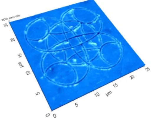
In order to illustrate the validity of the adopted CAD/CAM approach for AFM machining, a pattern already reported by Johannes et al. in [14] was designed as shown in Figure 2. In addition, the particular G-code that was fed to the developed post-processor is given in Table 1. It should be noted that the controller of the AFM instrument used in this study could only generate the lateral displacements of the AFM stage along four axes, namely in the directions perpendicular, parallel and at ± 45° angle with respect to the orientation of the long axis of the cantilever. Thus, to execute G-code instructions between points as accurately as possible, curves or lines representing planned tip trajectories have to be discretised into smaller segments oriented along one of these four constrained directions. In this study, such a discretisation step was achieved with the Bresenham’s line algorithm, which is commonly used in computer graphic applications. Finally, based on preliminary trial experiments, it was decided to process the designed pattern with a normal applied force set at 12 μN and with a Bresenham discretisation step of 100 nm. Figure 3 shows an AFM image of the obtained result.
Laser Metrology and Machine Performance XI
Table 1. G-code utilised G-code instructions G0 X-4.800 Y-4.800 G2 X4.800 Y4.800 I4.800 J4.800 G2 X-4.800 Y-4.800 I-4.800 J-4.800 G0 X4.800 Y-4.800 G3 X-4.800 Y-4.800 I-4.800 J-7.200 G3 X-4.800 Y4.800 I-7.200 J4.800 G3 X4.800 Y4.800 I4.800 J7.200 G3 X4.800 Y-4.800 I7.200 J-4.800 G0 X-10.124 Y5.476 G3 X-5.476 Y10.124 I2.924 J1.724 G0 X5.476 Y10.124 G3 X10.124 Y5.476 I1.724 J-2.924 G0 X10.124 Y-5.476 G3 X5.476 Y-10.124 I-2.924 J-1.724 G0 X-5.476 Y-10.124 G3 X-10.124 Y-5.476 I-1.724 J2.924 G0 X0.186 Y6.786 G2 X0.186 Y-6.786 I-19.386 J-6.786 G2 X-6.786 Y0.186 I-4.986 J1.986 G2 X6.786 Y0.186 I6.786 J-19.386 G2 X-0.186 Y-6.786 I-1.986 J-4.986 G2 X-0.186 Y6.786 I19.386 J6.786 G2 X6.786 Y-0.186 I4.986 J-1.986 G2 X-6.786 Y-0.186 I-6.786 J19.386 G2 X0.186 Y6.786 I1.986 J4.986 G0 X0.000 Y0.000
4
Conclusions
The aim of this study was to demonstrate the feasibility of applying a simple and generic CAD/CAM approach when implementing AFM probe-based nano-machining for producing 2D features with a commercial AFM instrument. This was realised using freely available CAD/CAM solutions during the design and tip trajectory planning stages of the process. This study suggests that through the utilisation of CAD/CAM software tools and commonly used file formats for software communication, it is possible to provide a high level of automation and flexibility for designing 2D nano-scale patterns and subsequently planning the corresponding AFM machining tasks.
However, it is anticipated that, when deploying this approach with any AFM instrument, it is still necessary to develop initially a post-processor that can translate the G-code format into instructions that can be understood by the AFM controller. This is due to the fact that conventional AFM systems are not developed with the primary purpose of conducting nano machining operations
Laser Metrology and Machine Performance XI
and understandably, they do not have built-in capabilities to read G-code input. In this research, this necessary link was established via the development of a C++ based post-processor for the AFM equipment controller in order interpret the G-code representation of tip path trajectories generated using the CAM software employed.
5
References
[1] Binnig G, Quate C and Gerber C 1986 Atomic force microscope Physical Review Letters 56(9) 930-934
[2] Tseng A, Notargiacomo A and Chen T 2005 Nanofabrication by scanning probe microscope lithography: a review J. Vac. Sci. Technol. B 23(3) 877-894
[3] Xie X, Chung H, Sow C and Wee A 2006 Nanoscale materials patterning and engineering by atomic force microscopy nanolithography Materials Science and Engineering R54 1-48
[4] Tseng A 2011 Removing material using atomic force microscopy with single- and multiple-tip sources Small 7(24) 3409-3427
[5] Jung T, Moser A, Hug H, Brodbeck D, Hofer R, Hidber H and Schwarz U 1992 The atomic force microscope used as a powerful tool for machining surfaces Ultramicroscopy 42 1446-1451
[6] Jin X and Unertl W 1992 Submicrometer modification of polymer surfaces with a surface force microscope Applied Physics Letters 61(6) 657-659 [7] Kim Y and Lieber C 1992 Machining oxide thin films with an atomic force
microscope: pattern and object formation on the nanometer scale Science
257(5068) 375-377
[8] Brousseau E, Krohs F, Caillaud E, Dimov S, Gibaru O and Fatikow S 2010 Development of a novel process chain based on atomic force microscopy scratching for small and medium series production of polymer nano structured components ASME Trans. Int. J. Mfg. Sci. 132(3) 030901 [9] Horcas I, Fernández R, Gómez-Rodríguez J, Colchero J, Gómez-Herrero J
and Baro A 2007 WSXM: a software for scanning probe microscopy and a tool for nanotechnology Review of Scientific Instruments 78 013705 [10] Lekki J, Kumar S, Parihar S, Grange S, Baur C, Foschia R and Kulik A
2004 Data coding tools for color-coded vector lithography Review of Scientific Instruments 75(11) 4646-4650
[11] Klehn B and Kunze U 1999 Nanolithography with an atomic force microscope by means of vector-scan controlled dynamic plowing J. Appl. Phys. 85(7) 3897-3903
[12] Cruchon-Dupeyrat S, Porthun S and Liu G 2001 Nanofabrication using computer-assisted design and automated vector-scanning probe lithography Applied Surface Science 175-176 636-642
[13] Xu K, Yang S and Qian X 2013 Integrating computer-aided design and nano-indentation for complex lithograph ASME Transactions, Journal of Micro and Nano-Manufacturing 1 011002
Laser Metrology and Machine Performance XI
[14] Johannes M, Kuniholm J, Cole D and Clark R 2006 Automated CAD/CAM-based nanolithography using a custom atomic force microscope IEEE Trans. Automation Sci. and Eng. 3(3) 236-239
[15] Johannes M, Cole D and Clark R 2007 Three-dimensional design and replication of silicon oxide nanostructures using an atomic force microscope Nanotechnology 18(34) 345304