To link to this article: DOI: 10.1016/j.ssi.2011.05.012
URL :
http://dx.doi.org/10.1016/j.ssi.2011.05.012
This is an author-deposited version published in:
http://oatao.univ-toulouse.fr/
Eprints ID: 5691
To cite this version:
Li, Rong and Zhen, Quiang and Drache, Michel and Rubbens, Annick and
Estournès, Claude and Vannier, Rose-Noëlle Synthesis and ion
conductivity of (Bi2O3)0.75(Dy2O3)0.25 ceramics with grain sizes from
the nano to the micro scale. (2011) Solid State Ionics, vol. 198 (n°1). pp.
6-15. ISSN 0167-2738
O
pen
A
rchive
T
oulouse
A
rchive
O
uverte (
OATAO
)
OATAO is an open access repository that collects the work of Toulouse researchers
and makes it freely available over the web where possible.
Any correspondence concerning this service should be sent to the repository
administrator:
[email protected]
Synthesis and ion conductivity of (Bi
2
O
3
)
0.75
(Dy
2
O
3
)
0.25
ceramics with grain sizes
from the nano to the micro scale
Rong Li
a,b, Qiang Zhen
a,⁎
, Michel Drache
b, Annick Rubbens
b, Claude Estournes
c, Rose-Noëlle Vannier
b,⁎⁎
a
Nano-science and Nano-technology Research Center, School of Materials Science and Engineering, Shanghai University, Shanghai 200444, PR China
bUniv. Lille Nord de France, CNRS UMR 8181, Unité de Catalyse et de Chimie du solide, Ecole Nationale Supérieure de Chimie de Lille, 59652 Villeneuve d'Ascq Cedex, France cPlateforme de Frittage Flash, PNF2, CIRIMAT, 118, route de Narbonne, 31062 Toulouse, France
a b s t r a c t
Keywords: Bi2O3–Dy2O3 Nano-crystalline ceramic SPS Pressureless sintering Oxide ion conductivityUsing (Bi2O3)0.75(Dy2O3)0.25nano-powder synthesized by reverse titration co-precipitation method as raw
material, dense ceramics were sintered by both Spark Plasma Sintering (SPS) and pressureless sintering. According to the predominance area diagram of Bi–O binary system, the sintering conditions under SPS were optimized. (Bi2O3)0.75(Dy2O3)0.25ceramics with relative density higher than 95% and an average grain size of
20 nm were sintered in only 10 min up to 500 °C. During the pressureless sintering process, the grain growth behavior of (Bi2O3)0.75(Dy2O3)0.25followed a parabolic trend, expressed as D2−D02= Kt, and the apparent
activation energy of grain growth was found to be 284 kJ mol−1. Dense (Bi
2O3)0.75(Dy2O3)0.25ceramics with
different grain sizes were obtained, and the effect of grain size on ion conductivity was investigated by impedance spectroscopy. It was shown that the total ion conductivity was not affected by the grain size down to 100 nm, however lower conductivity was measured for the sample with the smallest grain size (20 nm). But, although only the δ phase was evidenced by X-ray diffraction for this sample, a closer inspection by Raman spectroscopy revealed traces of α-Bi2O3.
1. Introduction
Bi2O3based materials are considered as potential solid electrolyte
materials at intermediate temperatures for use in catalytic membrane reactors, oxygen pumps and electrochemical sensors, since they exhibit higher oxygen ion conductivity than YSZ[1–3]. Indeed, with a value of 1 S cm−1at 800 °C, the ion conductivity of δ-Bi
2O3is likely
the highest one that can expect in an oxygen ion conductor [4]. However, this δ phase is only stable in a narrow temperature range (730 °C to 830 °C), limited by a dramatic phase transition and its melting point [5]. To stabilize this δ-form at lower temperature, numerous metal oxides were selected for substitution. Among these, Ln2O3 (Ln = Y, Ho, Er, etc.) were effective additives. According to
Nakayama[6], (Bi2O3)0.75(Dy2O3)0.25exhibits the best ion
conductiv-ity when compared to Y, Ho, Er and Yb doped compounds. It belongs to a (Bi2O3)1 − x(Dy2O3)xsolid solution with x between 0.222 and
0.292. However, as claimed by Watanabe[7], these stabilized δ forms are often metastable, due to an ordering of oxygen vacancies at
temperatures lower than 500 °C, which may lead to the formation of a rhombohedral phase to which corresponds the stoichiometric Bi7Ln2O13.5(x = 0.222) composition [8–10]. However, as shown by
several studies, one can expect to slow down the kinetics of phase transformation by decreasing the grain size of ceramics. A typical example is the tetragonal-monoclinic phase transition in zirconia-based ceramics[11–13]. It was shown that the tetragonal form of zirconia, which is stable above 1200 °C, could be stabilized at room temperature by decreasing the grain size below 30 nm. This was explained by excess surface energy, owing to the fact that the high temperature form adds a reduced surface energy with respect to the low temperature structure. With larger grain sizes, Fonseca et al.[14]
reported that the high temperature form of Bi26Mo10O69 was
stabilized in a larger temperature domain for ceramic with grain size of 1 μm compared to ceramics with larger grain size. The same conclusion was derived for the rhombohedral Bi–Sr–O type phase in the Bi2O3–La2O3system [15]. For Bi4La2O9, the kinetics of
transfor-mation of the β2phase to a monoclinic phase (ε) was shown to be
slowed down for ceramics prepared from attrition-milled powder in respect to ceramics prepared from coarse powder.
Nanocrystalline materials have attracted much attention, because of their specific properties in optical, electronic, magnetic and mechanical applications[16–18]. Reduction of grain size to the nano-scale leads to improvements by increasing the number of atoms in the grain ⁎ Corresponding author. Tel.: +86 21 66133800; fax: +86 21 66135215.
⁎⁎ Corresponding author. Tel.: +33 3 20436814; fax: +33 3 20436583.
E-mail addresses:[email protected](Q. Zhen),[email protected]
(R.-N. Vannier).
boundary. The effect of grain size on ion conductivity of polycrystalline material was also widely studied. Some results showed that the ion conductivity decreased with the decrease of grain size, while, according to some authors, a beneficial grain size effect could be observed when grain size was below 100 nm. At 300 °C, Ramamoorthy et al. measured, for 12 mol% Y2O3stabilized ZrO2nanocrystalline ceramic, 103 times
higher ion conductivity than for the microcrystalline ceramic[19]. The same phenomenon was observed for CeO2with grain size of 10 nm[20],
it was explained by an enhancement of the electronic conductivity when the grain size decreased below 100 nm. For Gd-doped CeO2,
an increase of the ion conductivity was noticed as the grain size decreased[21]. Based on the Brick layer model, assuming that all the grains are cubic with equal size, the grain size (dg) is much bigger than
the grain boundary thickness (δgb), and that the contribution of the
conductivity parallel to the grain boundary is negligible, the specific grain boundary conductivity can be estimated by the following equation [22]:
σspgb= σgb
δgb
dg:
Based on this relationship, in their report on tetragonal zirconia, Guo et al. showed that the specific grain boundary conductivity increased when the grain size decreased[23].
However, more recently, De Souza et al. on YSZ ceramics with grain size of 50 nm, found no evidence of fast diffusion along grain boundaries[24].
For δ-Bi2O3–Ln2O3 materials, which have the same fluorite
structure as YSZ with better ion conductivity, the effect of grain size on its electrical properties has not been reported yet.
To fabricate nanocrystalline ceramic, sintering process is an important step. When using rapid sintering technique such as Spark Plasma Sintering (SPS), one can expect to maintain the nano size of the grains in dense ceramics[25–27].
In this work, with the aim to study the effect of grain size on ion conductivity and stability, dense (Bi2O3)0.75(Dy2O3)0.25ceramics with
different grain sizes were prepared by SPS and pressureless sintering from nanopowders obtained as described in [28]. Moreover, the experimental conditions under SPS were optimized, and the densi-fication and grain growth behavior during the pressureless sintering process were studied. Finally, after a study on the stability of the
ceramics, the effect of grain size on oxygen ion conductivity was investigated by impedance spectroscopy.
2. Experimental 2.1. Sample preparation
(Bi2O3)0.75(Dy2O3)0.25 nanopowders were synthesized by a
reverse titration co-precipitation method as described in[28]. After annealing at 500 °C for 3 h, the powders exhibited the β-phase and one could not discard the possibility of δ-phase in the mixture. As shown in XRD patterns and TEM[28], the powder was composed of single crystal grains with an average size of 17 nm.
In order to obtain nanocrystalline (Bi2O3)0.75(Dy2O3)0.25ceramics,
the nanopowders were sintered by SPS (Dr. Sinter 2080 instrument, Syntex Inc. Japan) at the Plateforme Nationale de Frittage Flash du CNRS (PNF2) in Toulouse. About 0.8 g nanopowder was poured into a graphite die with an inner diameter of 8 mm. To avoid contamination, the die walls were protected with graphite foils. The SPS apparatus was run under temperature control. The heating process was controlled by a K type thermocouple put in a hole on the side of the graphite die. Experiments were carried out under pulsed DC current with a 12–2 sequence, 12 pulses of 3.3 ms spaced with 2 dead pulses. The period was therefore of 14 × 3.3 ms. During the experiment the current intensity reached 240 A at maximum.
(Bi2O3)0.75(Dy2O3)0.25 ceramics with larger grain size were
obtained by pressureless sintering. Green bodies with a relative density around 60% were prepared by uniaxial pressing at very low
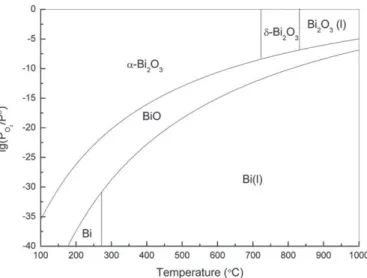
Fig. 2. Evidence of bismuth balls after the first Spark Plasma Sintering trial.
Fig. 3. Predominance diagram for Bi–O binary system. Fig. 1. Axial displacement of (Bi2O3)0.75(Dy2O3)0.25under 50 MPa with a heating rate of
100 °C/min under a 2–3 Pa Ar pressure (oxygen partial pressure 10−11bar) during
pressure followed by cold isostatic pressing at 170 MPa for 10 min. With a heating rate of 5 °C/min, the green bodies were sintered at 700 °C, 750 °C and 800 °C with various dwelling time to study the grain growth behavior and densification.
In order to compare ion conductivity, micro-crystalline (Bi2O3)0.75
(Dy2O3)0.25 powder was prepared by solid route at 800 °C, using
analytical pure Bi2O3, Dy2O3 as raw materials. By conventional
sintering (900 °C for 2 h), a dense ceramic with relative density of 94.21% was obtained.
2.2. Materials characterization
Phases of sintered samples were characterized by X-ray diffraction (D8 Advance AXS Bruker diffractometer equipped with a Vantec1de-tector (λCuKα= 1.5406 Å)). Data were collected in the 20° ≤2θ ≤ 80°
domain, with a 0.0148° step size and a counting time of 0.5 s per step. A LaB6standard was used to derive the instrument resolution. The
crystallite size was calculated using the Scherrer Equation D = 0.89λ/ (βcosθ) where β is the full width at half maximum of Bragg peaks.
The final density of pellets after sintering was measured by the Archimede method. Micrographs of sintered samples were observed by high resolution scanning electron microscopy (JSM-6700 F).
Ion conductivity of (Bi2O3)0.75(Dy2O3)0.25ceramics were
investi-gated by AC impedance spectroscopy, the measurements were carried out using a computer-controlled Solartron 1260 impedance analyzer with a 200 mV amplitude signal in the 1–106Hz frequency range from
200 °C to 500 °C at 25 °C intervals. A gold paste was used for electrodes. It was painted on both faces of the disk-shape samples, and annealed at 400 °C for 30 min. The annealing temperature of 400 °C was chosen after a thermogravimetric analysis of the gold paste, which shows that no weight loss was observed at temperature higher than 400 °C. In the measurements, pellets were placed between two gold electrodes using a homemade set-up. A thermocouple was positioned close to the samples to monitor the temperature. Then, the impedance spectra were analyzed using the Equivcrt software[29].
Fig. 5. XRD patterns of (Bi2O3)0.75(Dy2O3)0.25sample sintered by SPS (* peak caused by
the sample holder).
Fig. 6. Variation of crystallite size of (Bi2O3)0.75(Dy2O3)0.25samples at 700 °C, 750 °C and
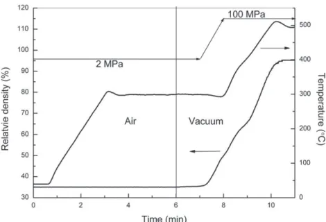
800 °C in function of sintering time (R values attest for the linear regression reliability). Fig. 4. Optimized sintering program and relative density of (Bi2O3)0.75(Dy2O3)0.25versus time under SPS.
3. Result and discussion 3.1. Spark plasma sintering
One of the main difficulties with Bi2O3-based materials is their
sensitivity towards reduction. As a rapid sintering technique, SPS was selected to avoid the grain growth. However, SPS is usually performed under vacuum, while under this condition, Bi2O3may easily reduce to
Bi metal, which is liquid at temperatures higher than 271 °C.
Fig. 1shows the corresponding linear shrinkage curves of (Bi2O3)0.75
(Dy2O3)0.25under a load of 50 MPa, with a heating rate of 100 °C/min
and a 2–3 Pa Ar pressure (oxygen partial pressure 10−11bar). The
displacement of 0.37 mm observed from room temperature to 200 °C was due to the compaction of the powder caused by the applied load, while the displacement observed from 400 °C to 550 °C was caused by the densification process. At about 700 °C, an accident in the shrinkage curve was evidenced, fumes were also noticed, therefore the experi-ment was stopped at 900 °C urgently, and then the sample was allowed cooling down. After the experiment, small balls of bismuth metal (seen inFig. 2) were found at the edge of the graphite die, and confirmed the reduction of bismuth.
The reduction of Bi2O3was verified by thermodynamic analysis.
Fig. 3gives the predominance diagram of Bi–O binary system. From
Fig. 3, when oxygen partial pressure lowered to 10−11bars, with
temperature increase, Bi2O3reduces to BiO around 530 °C, then BiO
further reduces to Bi at about 730 °C. This temperature is in good agreement with the experimental results.
According to the results above and considering that the release of CO2 from the powder, which may be carbonated, may disrupt the
sintering, it was decided to program a 5 min plateau at 300 °C. Details of the designed sintering program is shown inFig. 4: The temperature was first increased to 300 °C with a rate of 100 °C/min and maintained at 300 °C for 5 min; then the temperature was increased to 500 °C in 2 min and maintained for 1 additional minute. The experiment was carried out under air during the 5 first minutes before pumping out. A load of 2 MPa was applied during the 7 first minutes of experiment, then increased to 100 MPa in 1 min and maintained. The relative density of sample as a function of time is also given inFig. 4. The shrinkage after 7 min was due to the increase of the applied pressure, the densification started at the 8th minute and ended after the 10th minute. At the end of the sintering, the relative density of the sample reached 95%.
Fig. 5 shows the XRD patterns of (Bi2O3)0.75(Dy2O3)0.25 sample
sintered by SPS, it exhibits δ phase whereas β phase was observed for the powder. Using the Scherrer equation, an average crystallite size of 20 nm was derived, in good agreement with SEM, which revealed a dense ceramic with grains in the range of 20 nm, indicating that the grains were likely single crystals.
3.2. Pressureless sintering 3.2.1. Grain growth behavior
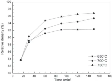
Since previous dilatometry study in[28]had shown that, for this powder, shrinkage under air started around 525 °C, with a maximum shrinkage rate at 700 °C, it was decided to follow the grain growth behavior of this ceramic at 650 °C, 700 °C and 750 °C. The variations of crystallite size of (Bi2O3)0.75(Dy2O3)0.25 samples as a function of
dwelling time at 650 °C, 700 °C and 750 °C are presented inFig. 6. At 650 °C, small traces of the rhombohedral β2phase were found, in good
agreement with high temperature X-ray diffraction data carried out on powder in[28]. However, the main phase was the δ phase, so its crystallite size was still included in this study. FromFig. 6, it can be seen that the variation of grain size with dwelling time at each sintering temperature follows a parabolic trend and the rate of grain growth increases with temperature from a low value at 650 °C to an extremely high value at 750 °C.
The variation of crystallite size in a sintering process can be expressed by:
Dn−D
n
o= kt ð2Þ
where k is a rate constant of grain growth; D is the average crystallite size after sintering; D0 is the average initial crystallite size; t is the
sintering time. Here, the value of D0was 17 nm, which corresponded to
the average crystallite size of the nanopowder calcined at 500 °C for 3 h
[28]. The exponent, n, characterizes the rate controlling process: for Fig. 7. Variation of lnK as a function of 1000/T for (Bi2O3)0.75(Dy2O3)0.25samples (R value
attests for the linear regression reliability).
Fig. 8. Relative density of (Bi2O3)0.75(Dy2O3)0.25samples as a function of dwelling time
at 650 °C, 700 °C and 750 °C.
Table 1
Grain size and relative density of (Bi2O3)0.75(Dy2O3)0.25samples for different sintering
conditions.
Sample Grain size (nm) Relative density (%)
SPS 500 °C 1 min 20 95.3
700 °C 2 h 101 94.4
Pressureless sintering 750 °C 1 h 178 94.7
800 °C 1 h 400 95.5
n =2, grain growth is controlled by grain boundary diffusion, for n = 3 grain growth is controlled by volume diffusion or diffusion through liquid, and for n=4 grain growth is controlled by surface diffusion.
Using the grain size data inFig. 6, and Eq. (2), the best linear regression was found for n = 2 at each temperature (with R = 0.988 at 650 °C, R = 0.999 at 700 °C, R = 0.997 at 750 °C). This means that the grain growth of (Bi2O3)0.75(Dy2O3)0.25sample was controlled by mass
transport through the grain boundary.
The calculation led to the following equations representing the grain growth of (Bi2O3)0.75(Dy2O3)0.25at the three different sintering
temperatures. 650 BC: D2−D20= 19:42t ð3Þ 700 BC: D2−D20= 87:64t ð4Þ 750 BC: D2−D 2 0= 734:51t: ð5Þ
From the above equations, the rate constants of grain growth were 19.42, 87.64 and 734.51 nm2/min at 650 °C, 700 °C, and 750 °C,
respectively. According to the Arrhenius equation, the rate constant can be expressed as a function of the reciprocal of the absolute temperature according to the expression:
k = k0exp −ΔE RT
ð6Þ where k is the rate constant of grain growth, k0is a pre-exponential
constant, ΔE is the apparent activation energy, R is the universal gas constant and T is the absolute temperature.
Rearranging the above equation gives, lnk = ln k0+ −
ΔE RT
: ð7Þ
According to Eq.(7), the relationship between ln(k) and1000/T is expected to be linear. The evolution of ln(k) versus 1000/T is given in
Fig. 7, which corresponds to the following equation: lnk = 39:87−34:181000
T : ð8Þ
Eq.(8) yields the apparent activation energy (ΔE) for the grain growth of (Bi2O3)0.75(Dy2O3)0.25to be equal to 284 kJ/mol. Activation
energies in the same order of magnitude were obtained by Tekeil et al. for undoped c-ZrO2(298 kJ/mol)[30]and 8YSCZ (289 kJ/mol)[31]
whose grain growths were also controlled by mass transport through the grain boundary.
3.2.2. Density variation
The relative density of (Bi2O3)0.75(Dy2O3)0.25 samples after
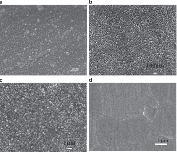
pressureless sintering as a function of dwelling time at 650 °C, 700 °C and 750 °C is given inFig. 8. The change rate of the relative density was extremely rapid in the early stage, and slowed down after 1 h. With same dwelling time, the relative density increased with sintering temperature obviously, indicating that sintering tempera-ture was a critical factor which influenced the relative density. The relative density of sample sintered at 650 °C was lower and did not satisfy the requirement for oxide ion conductivity measurements. Fig. 9. Microstructure of (Bi2O3)0.75(Dy2O3)0.25sintered samples (a) SPS, 500 °C/1 min, (b) 700 °C/2 h, (c) 800 °C/1 h, (d) 900 °C/2 h.
According to this study, powders were sintered at 700 °C for 2 h, 750 °C for 1 h and 800 °C for 1 h, in order to prepare dense ceramics with different grain sizes. The crystallite sizes of all pellets were calculated using the Scherrer equation. They are given inTable 1with the corresponding relative density of samples. The characteristics of the sample sintered from microcrystalline powder are also given. δ-phases were evidenced for all samples. Crystallite sizes ranged from 20 nm to the micron scale for the microscrystalline sample. Relative densities higher than 94% were obtained for all samples. The high density of samples was confirmed by SEM (Fig. 9).
3.3. Stability of ceramics
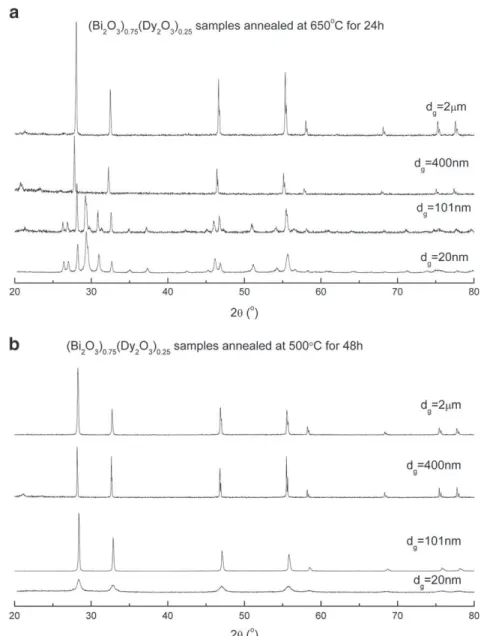
Prior to conductivity measurements, the stability of the dense ceramics was characterized. In a first step, samples with crystallite sizes of 20 nm, 101 nm, 400 nm and at the micron scale were annealed at 650 °C for 24 h. This temperature was chosen since it was shown that, on powder, the β phase transforms into a mixture of δ-type phase and rhombohedral β2-type phase between 620 °C and
720 °C[28]. The X-ray patterns of the ceramics with different grain size after annealing are given inFig. 10a. Although a better stability of
the ceramic could have been expected for ceramics with small grain size, here samples with the smaller grain sizes appeared to be less stable, with the appearance of β2phase after only 24 h of annealing. In
a second step, the stability of samples at 500 °C was also investigated. After 48 h at 500 °C, no evolution was observed and the microstruc-ture of samples was maintained (Fig. 10b). Therefore, it was decided to limit the impedance spectroscopy study to 500 °C.
3.4. Oxygen ion conductivity
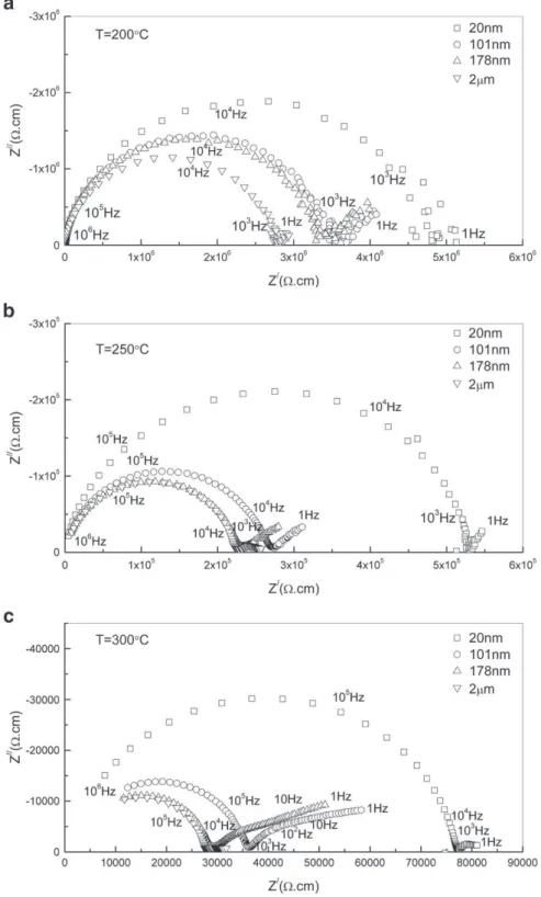
The impedance spectra of all samples at different temperatures are shown inFig. 11. Instead of three arcs as typical response of most ceramics, only two arcs were observed with capacitances of 10−11F and 10−6F for the high frequency arc and low frequency
arc, respectively, characteristic of the bulk response and the electrode response, respectively. Despite of the decrease of grain size and the concomitant increase of the grain boundaries, polarization effects of the grains and the grain boundaries could not be separated. Similar behaviors were also reported for Er2O3,
Y2O3 and MoO3 doped Bi2O3 materials [32–34]. At temperature
higher than 450 °C, only the electrode response was evidenced. Fig. 10. XRD patterns of (Bi2O3)0.75(Dy2O3)0.25samples after annealing (a) at 650 °C for 24 h and (b) at 500 °C for 48 h.
The diagrams were fitted with a resistance in parallel with a constant phase element. Characteristic parameters fitted at 300 °C for ceramics with different grain sizes are given inTable 2. A small increase of the resistance was observed when the grain size decreases with ideal capacitances (Y0) in the same order of
magnitude. From these data, the relaxation frequency (f0) and the
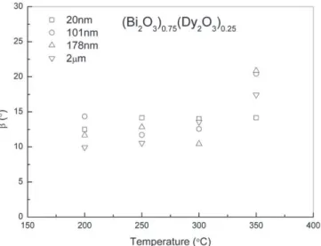
depression angle (β) were derived.Fig. 12shows the depression angle (β) value for (Bi2O3)0.75(Dy2O3)0.25samples as a function of
temperature. If β exceed 30°, one semicircle mode cannot be used to resolve the impedance diagrams. Here, for the temperatures below 300 °C, β was almost constant in the whole temperature
domain with a value lower than 15°, indicating that one circle model could be used for the analysis. For the temperatures higher than 350 °C, only the electrode response remained. The evolution of the relaxation frequency with temperature is given inFig. 13. This parameter is an intrinsic characteristic of the material, which could be used to describe phase transition. In this case, a linear evolution was observed and no phase transition was noticed during the experiment process.
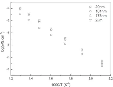
The Arrhenius plot of the conductivity is given inFig. 14 for all samples. Close activation energies were obtained with values of 1.08, 1.06, 1.08 and 1.02 eV from large grains to small grains. Despite close
conductivities were obtained for samples with grain size larger than 100 nm, the conductivity of the sample with the smallest grain size (20 nm) was clearly lower. At 500 °C, the total ion conductivity reached 10−2S cm−1for the samples with grain size higher than 100 nm and
3.1×10⁻³S cm−1 for the sample with grain size of 20 nm. This
decrease in ion conductivity could be due to an increase in the volume of the grain boundary with the reduction of grain size, which may become the limiting factor below 100 nm. The same effect was also observed in yttria doped zirconia ceramics, which exhibits the same
fluorite structure as δ-Bi2O3[35]. According to Peters et al., space charge
effect will be pronounced only in materials with low concentrations of mobile point defects[36]. For high ion conductors as bismuth based oxides, space charge effect is likely negligible and grain boundary resistance dominates when grain size decreases. However at that stage, one could not neglect the possibility of impurity. As mentioned above, X-rays revealed only a pure δ phase, but Bragg peaks were wide because of small grain size. Thus, to complete the study, Raman spectroscopy was carried out on the samples with grain size of 20 nm, 101 nm and Fig. 11 (continued).
400 nm, and compared to characteristic spectra of α-, β- and δ-Bi2O3
forms (Fig. 15). Despite pure δ phase was confirmed for samples with larger grain size, traces of α-Bi2O3were evidenced in the sample with
grain size of 20 nm. Therefore, one cannot exclude that this impurity could be the reason for the decrease in ion conductivity.
4. Conclusions
Combining SPS and pressureless sintering, dense samples with grain size varying from 20 nm to a few microns were prepared with close relative densities of about 95%. For pressureless sintering, the study of grain growth with dwelling time revealed that the grain growth of (Bi2O3)0.75(Dy2O3)0.25samples was controlled by mass transport through
the grain boundary. In contrast with what was expected from some literature data, the decrease of the grain size of the ceramic did not lead to a better stability of samples, since at 650 °C metastability was confirmed for samples with the smaller grain sizes (20, 101 nm). Although similar conductivities were obtained for samples with grain size larger than 100 nm, a decrease in ion conductivity was observed for the sample with grain size of 20 nm. As explained by Peters et al., space charge effect is likely negligible for such good oxygen ion conductor[36]. However, a closer inspection of this sample by Raman spectroscopy revealed traces of α-Bi2O3as impurity, which may be the reason of a lower conductivity.
Further experiments are in progress to optimize the sintering process and prepare pure δ ceramics with grain size lower than 100 nm.
Fig. 11 (continued).
Table 2
The equivalent circuit and parameter values for (Bi2O3)0.75(Dy2O3)0.25ceramics with different grain sizes.
Sample e/S (cm−1) Equivalent circuit Values of R (Ω), Y
0(F) and n (Bi2O3)0.75(Dy2O3)0.25at 300 °C dg= 20 nm 0.6257 (RQ) R = 4.85 × 10⁴, Y0= 1.22 × 10⁻¹¹, n = 0.9673 dg= 101 nm 0.3053 (RQ) R = 1.29 × 10⁴, Y0= 2.15 × 10⁻¹¹, n = 0.8604 dg= 178 nm 0.4233 (RQ) R = 1.13 × 10⁴, Y0= 1.33 × 10⁻¹¹, n = 0.8413 dg= 2 μm 0.3096 (RQ) R = 8.65 × 10³, Y0= 2.53 × 10⁻¹¹, n = 0.9466
Fig. 12. Evolution of the depression angle (β) with temperature for (Bi2O3)0.75
(Dy2O3)0.25samples with different grain size.
Fig. 13. Relaxation frequency determined from the impedance diagrams of (Bi2O3)0.75
Acknowledgments
Authors are grateful to the French Embassy in China for funding R. Li grant as a co-tutorial PhD between Shanghai University and the University of Lille.
The authors also thanks the Instrument Analysis Research Center of Shanghai University for their help in the characterization of materials (SEM, TEM, XRF) and the Plateforme Nationale de Frittage Flash du CNRS (PNF2) in Toulouse for SPS sintering.
The authors acknowledge the supports of National Nature Science foundation of China (no. 20101006, 51072112); Project of Shanghai
Municipal Education Committee; Magnolia Science and Technology Talent Fund (no. 2010B034), Science and Technology Commission of Shanghai Municipality; and Key Subject of Shanghai Municipal Education Commission (no. J50102).
References
[1] T.J. Huang, J.F. Li, J. Power Sources 181 (2008) 62–68. [2] Y. Li, C.Z. Wang, J. Rare Earth 26 (2008) 337–340.
[3] A.K. Rivai, T. Kumagai, M. Takahashi, Progr. Nucl. Energ. 50 (2008) 57–581. [4] M. Drache, P. Roussel, J.P. Wignacourt, Chem. Rev. 107 (2007) 80–96. [5] H.A. Harwig, A.G. Gerards, Thermochim. Acta 28 (1979) 121–131. [6] S. Nakayama, Ceram. Int. 28 (2002) 907–910.
[7] A. Watanabe, J. Solid State Chem. 40–41 (1990) 889. [8] M.J. Verkerk, A.J. Burggraaf, J Electrochem. 128 (1981) 75.
[9] H. Kruidhof, H.J.M. Bouwmeester, K.J. De Vries, P.J. Gellings, A.J. Burggraaf, Solid State Ionic 50 (1992) 181.
[10] K. Kruidhof, K.J. De Vries, A.J. Burggraaf, Solid State Ionic 37 (1990) 213. [11] E.C. Subbarao, A.H. Heuer, L.W. Hobbs, Advances in Ceramics v. 3: Science and
Technology of Zirconia I, The American Ceramic Society, Columbus, OH, 1981, pp. 1–24.
[12] R.C. Garvie, J. Phys. Chem. Solids 69 (1965) 1238–1241. [13] R.C. Garvie, J. Phys. Chem. 82 (1978) 218–224.
[14] F.C. Fonseca, M.C. Steil, R.N. Vannier, G. Mairesse, R. Muccillo, Solid State Ionics 140 (2001) 161–171.
[15] M. Drache, N. Djelal, M.C. Steil, P. Roussel, P. Conflant, Mater. Res. Bull. 40 (2005) 1599–1608.
[16] Y.J. Kang, H.J. Park, G.M. Choi, Solid State Ionics 179 (2008) 1602–1605. [17] T.M. Kamel, G. de With, J. Eur. Ceram. Soc. 28 (2008) 851–861. [18] K.T. Liu, J.G. Duh, J. Electroanal. Chem. 618 (2008) 45–52.
[19] R. Ramamoorthy, R.N. Viswanath, S. Ramasamy, Nanostruct. Mater. 6 (1995) 337–340.
[20] E.B. Lavik, Y.M. Chiang, Mater. Res. Soc. Symp. Proc. 457 (1997) 63–68. [21] T. Suzuki, I. Kosacki, H.U. Anderson, Solid State Ionics 151 (2002) 111–121. [22] M. Aoki, Y.M. Chiang, I. Kosacki, L.J.R. Lee, H. Tuller, Y. Liu, J. Am. Ceram. Soc. 79
(1996) 1169–1180.
[23] X. Guo, Z. Zhang, Acta Mater. 51 (2003) 2539.
[24] R.A. De Souza, M.J. Pietrowski, U. Anselmi-Tamburni, S. Kim, A.A. Munir, M. Martin, Phys. Chem. Chem. Phys. 10 (2008) 2067–2072.
[25] G.S. Kim, H.G. Kim, D.G. Kim, S.T. Oh, M.J. Suk, Y.D. Kim, J. Alloys Compd. 469 (2009) 401–405.
[26] J.T. Wang, D.L. Yin, J.Q. Liu, J. Tao, Y.L. Su, X. Zhao, Scr. Mater. 59 (2008) 63–66. [27] R. Chaim, M. Levin, A. Shlayer, C. Estournès, Adv. Appl. Ceram. 107 (2008) 159–169. [28] R. Li, Q. Zhen, M. Drache, A. Rubbens, R.N. Vannier, J. Alloys Compd. 494 (2010)
446–450.
[29] B.A. Boukamp, Solid State Ionics 20 (1986) 31–44.
[30] S. Tekeil, M. Erdogan, B. Aktas, Ceram. Int. 30 (2004) 2203–2209. [31] S. Tekeil, U. Demir, Ceram. Int. 31 (2005) 973–980.
[32] J.R. Macdonald, Impedance Spectroscopy, Wiley, New York, 1987.
[33] P. Duran, J.R. Jurado, C. Moure, N. Valverde, B.C.H. Steele, Mater. Chem. Phys. 18 (1987) 287–294.
[34] L.S. Wang, S.A. Barnett, J. Electrochem. Soc. 139 (1992) 2567–2572. [35] S. Boulfrad, E. Djurado, L. Dessemond, Fuel Cells 5 (2008) 313–321.
[36] A. Peters, C. Korte, D. Hesse, N. Zakharov, J. Janek, Solid State Ionics 178 (2007) 67–76. Fig.14. Temperature dependence of total ion conductivity of (Bi2O3)0.75(Dy2O3)0.25
samples with different grain size.
Fig. 15. Bi0.75Dy0.25O1.5Raman spectra of samples sintered by SPS (dg= 20 nm) and by
pressureless sintering at 700 °C (dg= 101 nm) and 800 °C (dg= 400 nm) compared to