Pépite | Propriétés électroniques de transistors à nanotubes de carbone couplés à des nanocristaux de semiconducteurs
110
0
0
Texte intégral
(2) Thèse de Ewa Zbydniewska, Lille 1, 2016. © 2016 Tous droits réservés.. doc.univ-lille1.fr.
(3) Thèse de Ewa Zbydniewska, Lille 1, 2016. WARSAW UNIVERSITY OF TECHNOLOGY Faculty of Physics. Ph.D. THESIS Ewa Zbydniewska, M.Sc., Eng. Electronic Properties of Coupled Semiconductor Nanocrystals and Carbon Nanotubes. Supervisors Mariusz Zdrojek, PhD, DSc (WUT) Thierry Mélin, PhD, DSc (IEMN). Warsaw, 2015. © 2016 Tous droits réservés.. doc.univ-lille1.fr.
(4) Thèse de Ewa Zbydniewska, Lille 1, 2016. © 2016 Tous droits réservés.. doc.univ-lille1.fr.
(5) Thèse de Ewa Zbydniewska, Lille 1, 2016. To my mother. © 2016 Tous droits réservés.. doc.univ-lille1.fr.
(6) Thèse de Ewa Zbydniewska, Lille 1, 2016. © 2016 Tous droits réservés.. doc.univ-lille1.fr.
(7) Thèse de Ewa Zbydniewska, Lille 1, 2016. Acknowledgements Firstly, I would like to express my sincere gratitude to my advisors, Dr Thierry Mélin and Dr Mariusz Zdrojek for the continuous support of my PhD study, for their patience, motivation, and tremendous knowledge. Their guidance helped me in all the time of research and writing of this thesis. I could not have imagined having better advisors and mentors for my PhD study. Special thanks to Thierry for believing in me and welcoming me in his group so it felt like home. I would like to acknowledge all persons who helped me during my PhD: I would like to thank to Djamila Hourlier for helping in sample preparation and for performing the TGA and Raman analysis; François Vaurette for his assistance with EBL and for guiding me in the clean-room; Dominique Deresmes, Stéphane Lenfant, Jarek Judek and Charlène Brillard for technical support; Ania Dużyńska and David Brunel for growing beautiful tubes; Michka Popoff for conducting the fluorescence experiments at the BioImaging Center Lille (BICeL) (Université Lille Nord de France); Florence Senez for taking good care of me and Moussa Biaye. Also, I would like to thank the team of engineers in the clean-room who trained me, helped me, and shared their knowledge of the different machines and technological processes so I was able to obtain these results. I am very grateful for all the help. I thank my fellow labmates and friends for the stimulating discussions, for the help and for all the fun we have had in the last years. I thank to: PAF and Ophélie, Di and Wei, Maciek and Kasia, Franek, Marek and Alice, Kim, Hind and Nadine, Abbas, Philipp and Anke, Fabio and Jenya, Ania Ł. I would like to thank my family: my parents and brother, especially to my mother – I wouldn't be where I am today if it wasn't for her. And last but not the least, to my husband Mathieu, for his optimism, patience and support, merci mon coeur.. VII © 2016 Tous droits réservés.. doc.univ-lille1.fr.
(8) Thèse de Ewa Zbydniewska, Lille 1, 2016. VIII © 2016 Tous droits réservés.. doc.univ-lille1.fr.
(9) Thèse de Ewa Zbydniewska, Lille 1, 2016. Abstract We study the electronic properties of coupled semiconductor nanocrystals and carbon nanotubes. We report measurements of single electron transfers between single CdSe colloidal nanocrystal coupled to a carbon nanotube field effect transistor at room temperature in ambient conditions. The measurements consist of nanotube current level monitoring as a function of time for fixed gate voltage. We observe a sequence of high - low currents (random telegraph signal) on time scales up to several seconds with ms sampling time. We attribute the two level current fluctuations to the transfer of single electron onto the nanocrystal. The probability of the occupation time τ at the high or low current state follows a power law of the form P(τ)~τ-α where exponent α lies between 1.5 and 4 (typically close to 2.8). The observation suggests that the two-level current switching is similar to the fluorescence intermittency (optical blinking) observed in individual quantum dots. The spectroscopic analysis of the devices based on coupled semiconductor nanocrystals and carbon nanotubes is consistent with the charging of nanocrystal defect states with a charging energy of Ec ~ 200 meV. The approach developed here enables to probe the trap state dynamics in quantum dots in ambient air and room temperature from a purely electrical approach, and therefore to better understand the physics at hand in (opto)electronic devices based on quantum dots.. IX © 2016 Tous droits réservés.. doc.univ-lille1.fr.
(10) Thèse de Ewa Zbydniewska, Lille 1, 2016. X © 2016 Tous droits réservés.. doc.univ-lille1.fr.
(11) Thèse de Ewa Zbydniewska, Lille 1, 2016. Résumé Ce travail de thèse décrit les propriétés électroniques de nanodispositifs couplés entre transistors à nanotubes de carbone (CNTFETs) et nanocristaux semiconducteurs colloïdaux CdSe/ZnS individuels en régime de détection de charge unique à température ambiante. Les transferts de charges élémentaires entre nanotubes et nanocristaux sont mis en évidence par les fluctuations temporelles du courant des transistors à tension de grille fixée, et font apparaître un signal à deux niveaux (bruit télégraphique ou RTS), observé sur des échelles de temps entre 1s et 0.1 ms. Les temps d’occupation τ des niveaux de courant suivent une loi de puissance P(τ)~τ-α où l’exposant α varie entre 1.5 et 4 (typiquement proche de 2.8). Cette observation suggère que les fluctuations de charges observées sont à la base des phénomènes de "clignotement optique" des nanocristaux colloïdaux étudiés. L’analyse spectroscopique des dispositifs permet d’attribuer ce clignotement à des pièges dans la bande interdite des nanocristaux, avec une énergie de chargement Ec de l’ordre de 200 meV. L’approche présentée dans ce travail peut être étendue à des mesures électro-optiques, et donc permettre une meilleure compréhension des phénomènes physiques contrôlant les propriétés optoélectroniques de nanodispositifs à base de nanocristaux semiconducteurs.. XI © 2016 Tous droits réservés.. doc.univ-lille1.fr.
(12) Thèse de Ewa Zbydniewska, Lille 1, 2016. XII © 2016 Tous droits réservés.. doc.univ-lille1.fr.
(13) Thèse de Ewa Zbydniewska, Lille 1, 2016. Introduction This Ph.D. thesis was completed under the joint doctorate according to cotutelle agreement between Université des Sciences et Technologies de Lille (USTL) and Faculty of Physics, Warsaw University of Technology in Poland (WUT).. The aim of this work was to make use of the unique carbon nanotubes (CNTs) properties in single electron detection performed during the measurements of electronic properties of single quantum dots (QDs). The aim of the work was divided between two Universities. First part was realized at the USTL in the Institute d'Electronique, de Microélectronique et de Nanotechnologie, where the nanodevices based on carbon nanotubes and quantum dots were fabricated. The second part was realized at WUT, where the devices were characterized. Both aims were achieved successfully and further studies on single electron transfer between single quantum dots and carbon nanotube based transistor was realized. This manuscript contains four chapters. The first chapter provides a general introduction to the theory of carbon nanotube field effect transistors (CNTFETs), with the description of fundamental properties of CNTs, analysis of the switching mechanism and characteristics of single-CNTFETs and efforts towards device integration. The second chapter is an introduction to the theory of semiconductor QDs. Its first part is enclosed with a short bibliography on quantum confinement in semiconductors, the QD synthesis, and description of core-shell QDs. Its second part reports about the confocal luminescence experiments and the electrical measurements revealing optical blinking of semiconductor QDs, a two-state system intermittency, in which the light emission from a QD is switched on and off by the fluctuation of the charge occupation of a single electronic state. Section 2.3 provides a short state of art on the electronic properties of devices coupling QDs and CNTs. A methodology of device preparation and characterization is introduced in Chapter 3. Essentially, a nanodevice is composed of a single CNT coupled to a QD under investigation. Such a hybrid structure allows to manipulate single electrons in a nanoparticle in a controllable way. Finally, Chapter 4 contains a description of the experiments made during this PhD, followed by discussion and conclusions.. XIII © 2016 Tous droits réservés.. doc.univ-lille1.fr.
(14) Thèse de Ewa Zbydniewska, Lille 1, 2016. XIV © 2016 Tous droits réservés.. doc.univ-lille1.fr.
(15) Thèse de Ewa Zbydniewska, Lille 1, 2016. Contents Acknowledgements .............................................................................................................. VII Abstract .................................................................................................................................. IX Résumé ................................................................................................................................... XI Introduction ........................................................................................................................ XIII Chapter 1: Introduction to carbon nanotube field effect transistors ................................. 1 1.1 Carbon nanotubes ............................................................................................................. 3 1.1.1 Structural and electronic properties ............................................................................... 2 1.1.2 Carbon nanotube synthesis and dispersion ................................................................... 6 1.2 Transistors based on carbon nanotubes .......................................................................... 8 1.2.1 Electrical switching of CNTs......................................................................................... 9 1.2.2 Electronic transport ...................................................................................................... 11 1.2.3 Performance of CNTFETs ........................................................................................... 12 1.3 Nonvolatile memories based on carbon nanotubes ....................................................... 13 References .............................................................................................................................. 16 Chapter 2: Semiconductor nanocrystals ............................................................................. 21 2.1 Basics of semiconductor nanocrystals ........................................................................... 21 2.1.1 Quantum confinement in semiconductors .................................................................. 22 2.1.2 Quantum dot synthesis ................................................................................................ 23 2.1.3 Core-shell QDs ........................................................................................................... 24 2.2 Blinking of single QD ...................................................................................................... 26 2.2.1 Confocal luminescence experiments .......................................................................... 26 2.2.2 Electrical current switching in single QD ................................................................... 28 2.4 Electronic properties of coupled QDs and CNTs ......................................................... 30 References .............................................................................................................................. 36 Chapter 3: Fabrication of nanodevices based on CNTs and QDs .................................... 41 3.1 Fabrication of back-gated CNTFETs ............................................................................ 41 3.1.1 Markers fabrication ..................................................................................................... 42 3.1.2 CNTs deposition and growth ...................................................................................... 43 3.1.3 CNTs localization and contacts fabrication ............................................................... 47 XV © 2016 Tous droits réservés.. doc.univ-lille1.fr.
(16) Thèse de Ewa Zbydniewska, Lille 1, 2016. 3.2 Characterization of CNTFETs ....................................................................................... 48 3.2.1 Principle of electrical measurements .......................................................................... 48 3.2.2 Transport characterization .......................................................................................... 51 3.3 QDs deposition ................................................................................................................. 51 3.3.1 Fluorescence experiments ........................................................................................... 52 3.4 Issues in the nanofabrication of coupled QD-CNTFET devices ................................. 53 References .............................................................................................................................. 56 Chapter 4: Charge blinking of semiconductor nanocrystals probed by carbon nanotube field-effect transistors ............................................................................................................ 57 4.1 Coupled nanocrystal - nanotube field-effect transistor devices .................................. 57 4.2 Device characterization and random telegraph signal ................................................ 58 4.2 Device characterization and random telegraph signal ................................................ 58 4.3 NC-CNTFET spectroscopic analysis: trap-state charging energy ............................. 62 Discussion ............................................................................................................................... 74 References .............................................................................................................................. 76 Conclusions and perspectives ............................................................................................... 79 Annex A: Thermal analysis of nanotubes ........................................................................... 81 Annex B: Analysis of RTS in CNTFETs ............................................................................. 87 List of publications and communications ............................................................................ 93. XVI © 2016 Tous droits réservés.. doc.univ-lille1.fr.
(17) Thèse de Ewa Zbydniewska, Lille 1, 2016. Chapter 1. Introduction to carbon nanotube field effect transistors The field of the electronics has undergone in the last decades great progress with many benefits in the field of computing or communications, which affect every aspect of our modern lives. Advanced lithography instruments provide the ability to create incessantly smaller electronic devices. One of the finest examples of miniaturized devices is silicon-based field effect transistors (FETs), which have led to denser and faster integrated circuits.1 However, fundamental scientific and technological limitations will not enable to build better performing silicon devices below a certain size. Thus, researchers have taken considerable efforts to develop alternative device technologies based on low nanomaterials with low dimensionalities such as, for example, single-walled carbon nanotubes (SWCNTs) acting as one-dimensional semiconducting or metallic channels with adaptable electrical-transport properties. Carbon nanotube field effect transistors (CNTFETs) made from semiconducting SWCNTs have been demonstrated with nearly optimal and highly tunable properties. The next paragraphs of this introduction chapter contain a description of fundamental properties of carbon nanotubes (CNTs), the analysis of their switching mechanism, the characteristics of single-CNTFETs and the efforts made so far towards device integration. The following description is not exhaustive and it is only a guide to help to understand the final chapters of this work. For more detailed information the reader may refer to following authors: Tobias Dürkop form the University of Maryland in his review on carbon nanotubes high mobility2 and Phaedon Avouris from IBM Research Division in publications on nanotube-based electronics circuits.3,4,5. 1 © 2016 Tous droits réservés.. doc.univ-lille1.fr.
(18) Thèse de Ewa Zbydniewska, Lille 1, 2016. 1.1 Carbon nanotubes The first observation of CNTs is attributed to Sumio Iijima. In 1991, the Japanese scientist has published the first high resolution TEM images of “Helical microtubules of graphitic carbon”,6 and thus he introduced carbon nanotubes to the scientific world. Since then, carbon nanotubes have attracted great interest as they offer unique properties with a wide range of potential applications. 1.1.1 Structural and electronic properties Carbon nanotubes are members of the fullerene structural families of carbon (see Figure 1.1). They owe their name due to their long and hollow structure (a tube) formed from single layer(s) of hexagonally arranged carbon atoms (graphene). The structure of these nanomaterials is quasi-dimensional. The length-to-diameter ratio of CNTs could be very high, even up to 132 000 000:1,7 which is much larger than for any other known material.. Figure 1.1 Fullerene structural families. (a-f) Crystal structure of a few carbon allotropes: (a) Diamond, (b) Graphite, (c) Fullerene - C60, (d) Graphene, (e) SWCNT, (f) multi-walled CNT. Adapted from8,9. From a structural point of view, carbon nanotubes either correspond to single-walled nanotubes (SWCNTs) and multi-walled nanotubes (MWCNTs). The first one is, as described above, a tube with just one wall (layer). MWCNTs consist of multiple concentric tubes, as shown in Figure 1f. The distance between each concentric layer in MWCNTs is similar to the distance between each graphene layer in highly oriented pyrolitic graphite, which is around . Because of the complexity of their structure (mostly leading to a metallic 2 © 2016 Tous droits réservés.. doc.univ-lille1.fr.
(19) Thèse de Ewa Zbydniewska, Lille 1, 2016. behaviour) and the fact that MWCNTs often appear with structural defects, SWNTs have much better performance and are more suitable for transistor applications.10,11,12 Therefore, in this work only single-walled carbon nanotubes have been considered, and the abbreviation of CNTs will only refer to single walled carbon nanotubes throughout the rest of the manuscript. The best way to describe the structure of a CNT is to start with a single layer of graphene. Figure 1.2a presents the schematics of the hexagonal planar lattice with an indication of how to cut a narrow strip out from the graphene sheet in a given direction in order to roll it up to the form of a cylinder. One of the most striking property of CNTs is that the structure of CNTs (including their metallic or semiconducting character) depends on this chosen direction. The vector defining the CNT circumference is given by equation: , where numbers. and. and. are the unit vectors of the hexagonal planar lattice and the. are called the chirality indexes. Note that. and. describe the structure. For example, CNTs with indices. precisely determine and. are called armchair, those with. zigzag and other tubes are chiral (see Figure 1.2b). The chirality indexes can used to determine the diameter of a CNT from the following equation: , where. (1.1). is the nearest neighbor distance between carbon atoms.13. Figure 1.2 Structure of CNTs. (a) Hexagonal structure of graphene with its unit cell (gray rhombus) and base vectors. The. vector defines the circumference of the CNT and. represents its. chiral angle. The solid lines indicate the circumferences of a zigzag and an armchair CNT, and the dashed lines of a chiral CNT (vectors OT and OA). (b) Examples of the three types of CNTs. Adapted from14. 3 © 2016 Tous droits réservés.. doc.univ-lille1.fr.
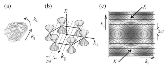
(20) Thèse de Ewa Zbydniewska, Lille 1, 2016. The electronic structure of carbon nanotubes can be obtained from the electronic structure of graphene. It turns out that by using a tight binding scheme, the variation of the energy as a function of the wave vector can be describe by the following formula: , where. (1.2). is the bond energy between carbon atoms. A positive sign in the equation 1.2. refers to the conduction band, while a negative sign refers to the valence band. The bands are in contact when. and the contact points are located at the vertices of the hexagons. forming the reciprocal lattice. The way to determine the band structure of a CNT is to use periodic boundary conditions along the nanotube edges, starting from the graphene band structure. The new wave vector has two components, a longitudinal one and perpendicular one (with respect to the circumference of the nanotube): .. (1.3). From the fact that the CNT length is much bigger than its diameter it can be assumed that the wave vector along the nanotube axis can take random real values. In contrary, in a perpendicular axis direction, the wave vector is quantized. Compared to the reciprocal graphene lattice, the allowed states lay on parallel lines along the value of. direction separated by. (see Figure 1.3).. Figure 1.3 Electronic properties of CNTs. (a) Diagram of a CNT with marked directions of and wave vectors. (b) Band structure of graphene determined by equation 1.2 in a conical representation. The wave vectors. are indicated by lines, separated by. Brillouin zone with allowed. . (c) The. conduction band mapped to the first. indicated by horizontal lines and marked K points. Adapted from. 8. 4 © 2016 Tous droits réservés.. doc.univ-lille1.fr.
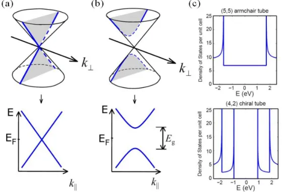
(21) Thèse de Ewa Zbydniewska, Lille 1, 2016. The CNT band structure is formed by the intersection of the If at least one allowed. line crosses the. or. values and the. surface.. points in the first Brillouin zone it indicates. that the nanotube is metallic (Figure 1.4a). In other cases an energy gap appears in the band structure and the carbon nanotube is semiconducting (Figure 1.4b). It can be proven that if the chirality indices meet the condition or. , where is the integer, the. line crosses the. , the CNT is semiconducting.15. point. In case when. Figure 1.4 Band structure of CNTs. Conical band structure with allowed wave vector of (a) metallic and (b) semiconducting CNT. (c) Density of states for a (5,5) metallic and a (4,2) semiconducting CNT. 8 Adapted from. The density of states (DOS) is another important feature affecting electronic properties of carbon nanotubes. Figure 1.4c presents an example of the density of states for metallic and. semiconducting CNT. One can observe the sharp peaks called van Hove. singularities which are characteristic of 1D systems.16 With the parabolic band approximation, the DOS function is. . For metallic nanotubes, the DOS near the Fermi level is. approximately constant and for semiconducting nanotubes, the DOS is equal to zero, forming a band gap. It should be noted that van Hove singularities exist for the energy for which the corresponding subband has the minimum. In the case of CNTs with similar diameters, chiral nanotubes have more peaks than the armchair. The local density of states can be determined experimentally by STM spectroscopy.17. 5 © 2016 Tous droits réservés.. doc.univ-lille1.fr.
(22) Thèse de Ewa Zbydniewska, Lille 1, 2016. 1.1.2 Carbon nanotube synthesis and dispersion The three main and most common methods used in the synthesis of CNTs are: arc discharge, laser ablation and chemical vapor deposition (CVD). The first MWNTs have been noticed in the material created after an arc discharge experiment.6 An electrical discharge can be induced by applying a high voltage between two graphite rods, which creates a plasma of carbon molecules. MWCNTs and SWNTs can be formed by this process if the rods contain metal catalyst such as nickel, iron or cobalt.18 In the laser ablation method a high energy pulsed laser is used to irradiate a carbon target containing Ni and Co instead of an electrical discharge to create the plasma for the CNT growth. 19 These two methods are often used to produce CNTs, however with the drawback that they form bundles of CNTs with mixed undesired structures formed by carbon or metal particles. Nowadays, the production of CNTs is mostly done using CVD methods. The main advantage of CVD, with respect to our work, is that it gives the possibility to grow CNTs directly at a specific position on a given substrate, which is very helpful in the fabrication of devices based on single CNTs. A disadvantage of CVD will be of course that this technique produces both semiconducting and (in our work, unwanted) metallic nanotubes, which need to be sorted out by electrical characterization. In practice, during the CVD process, a substrate is prepared from a layer of metal catalyst nanoparticles, generally Ni, Co,20 Fe, or a combination of these elements.21 The diameters of CNTs grown from such catalysts depend to the size of the original metal particles, which can be controlled e.g. when starting from patterned metallic layers. The substrate is preheated to around. , and the growth of nanotubes is done in a. reactor with a flow of two gases: a process gas like ammonia, nitrogen or hydrogen and a gas containing the carbon element like acetylene, ethylene or methane. The nanotubes grow from the sites of metal catalysts, where the carbon-containing gas is dissociated. The metal catalyst particles are located after growth either at the apex of the grown CNTs, or at the CNT bottom.22 In our work we used CNTs from a growth process via a catalytic CVD technique using pure methane (CH4) as the carbon source.23 The procedure of catalyst growth is described in chapter 3 (see 3.1.2 CNTs deposition and growth section). Unfortunately, a complete control of the nanotube growth process is not possible using the above mentioned synthesis methods. Consequently, the growth of CNTs is more or less non-selective with respect to chirality and diameter distribution.24 This is a major issue, as the use of nanotubes in various advanced electronic applications requires carbon nanotubes with specific diameters and chirality, and, in particular, in our case, to use only semiconducting 6 © 2016 Tous droits réservés.. doc.univ-lille1.fr.
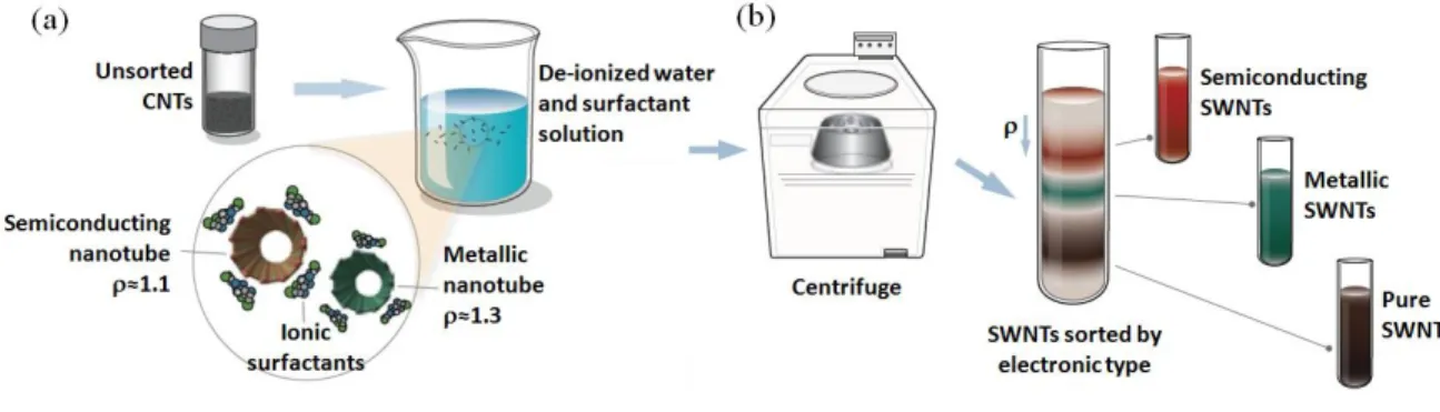
(23) Thèse de Ewa Zbydniewska, Lille 1, 2016. rather than metallic nanotubes. A lot of efforts have been spent on the development of more selective methods for CNTs synthesis and also on the development of dispersion and sorting techniques. The Hersam Research Group at Northwestern University has developed a technology known as density gradient ultracentrifugation (DGU)25 for separating carbon nanotubes by their optical and electronic properties. A company (NanoIntegris) was established to commercialize this technology.26 The DGU process can be described as follows: the unsorted CNT material is placed in an aqueous solution containing a combination of surfactants (surface active reagents). Surfactants adhere selectively to CNTs of different species. This process helps to enhance the effective density difference between them (Figure 1.5a). The obtained solution is then centrifuged under a high centrifugal field. The CNTs covered with surfactants migrate during the spinning process to their isopycnic (same density) point in the density gradient. Once semiconducting CNTs are spatially separated from the metallic ones, they can be isolated using established fractionation techniques (Figure 1.5b). The collected semiconducting CNTs can then be ‘dried’ in the form of a powder, which can be later be used in the same way as the nanotube powder obtained from arc-discharge and laser ablation methods, by a further dispersion into organic solvents.. Figure 1.5 Scheme of processing flow for the NanoIntegris technology for separating CNTs by their optical and electronic properties. (a) CNTs dispersed in aqueous solution using a combination of surfactants. (b) 26 Separated CNTs after centrifugation process. Adapted from. To do this, the most commonly used method to disperse CNTs is ultrasonication in an organic solvent.27,28 Bahr et al.29 described the solubility of small diameter SWNTs in organic solvents including 1,2-Dichlorobenzene. It was suggested that impurities (amorphous carbon and metal catalysts) take part in the dispersion of SWNTs. The nanotube purification process may in a reversed way modify their solubility properties. Koshio et al.30 reported that the ultrasonication of SWNTs in a monochlorobenzene solution of poly(methyl methacrylate) followed by a filtration step is an effective way to purify SWNTs. It was also found that SWNTs react chemically with the organic liquids during ultrasonication. Niyogi et al. studied 7 © 2016 Tous droits réservés.. doc.univ-lille1.fr.
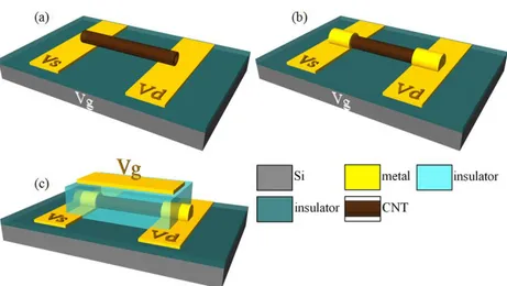
(24) Thèse de Ewa Zbydniewska, Lille 1, 2016. the nature of SWNT-organic solvent interaction that is responsible for the stabilization of ultrasonicated dispersions.27. 1.2 Transistors based on carbon nanotubes Since the first observation of carbon nanotubes in 1991, scientists have taken a lot of effort to use this unique material in electronics. This mission is particularly important, because further scaling of classical silicon based field effect transistors will be ultimately limited by top-down fabrication technology and silicon intrinsic electronic performances. Using CNTs with diameters of ~1 nm instead of silicon-based field effect devices would reduce the dimensions of transistors and thus increase the packing of integrated circuits. One of the first field effect transistors with a single semiconducting CNT channel (CNTFET) was introduced in 1998 by Tans et al. at Delft University of Technology. 31 The nanotube was placed on top of an oxidized silicon substrate with predefined platinum contacts. In such a device geometry, the current flow through the nanotube, and the bottom side of the sample works as an electrostatic gate that can be used for current modulation. The performance of the first CNTFETs was far from ideal, with a large contact resistance, low drain current and low conductance. Many techniques were introduced in order to improve their electrical characteristics. For example: the use of low work-function metal contact as compared to CNTs work function;32 the annealing of contacts in order to alter the nanotube– metal bond; the reduction of the thickness of the dielectric layer; the use of new transistor geometries. Figure 1.6 shows schematically three different CNTFET geometries: back gate geometries with CNT deposited on top of the metal contacts (a), 33 CNT covered with metal contacts (b)34 and a top gated CNTFET (c).35. 8 © 2016 Tous droits réservés.. doc.univ-lille1.fr.
(25) Thèse de Ewa Zbydniewska, Lille 1, 2016. Figure 1.6 Different geometries of CNTFETs. Back gate geometries with (a) CNT deposited on top of the metal contacts and (b) CNT covered with metal contacts; (c) FET geometry with a CNT covered with metal 33,34,35 contacts together with a top gate modulation. Adapted from. 1.2.1 Electrical switching of carbon nanotube field effect transistors Nowadays, field effect transistors (FETs) are based on silicon, and operate by switching between. and. states. Semiconducting CNTs can also be switched. and. and are hence suitable materials for FET applications.4 Two models were developed to explain the operation of CNTFETs: a classical MOSFET model and a Schottky barrier field effect transistor model.36 In the first model for the p-type CNTFET, the inversion layer is induced by applying negative gate potential ( ), and the potential difference between the source (S) and drain (D) electrodes causes the current flow – the transistor is switched The. .. adjustment influences the carrier (holes) concentration and thereby the transistor. resistance. The transistor is switched of an appropriate. when the depletion layer is formed upon application. . In the case of a CNTFET with Schottky barriers, the transistor operation. is based on the modulation of the potential barriers at the metal-nanotube junction. Since the CNT is connected from one side to the source electrode and at the other side to the drain, one have to consider two Schottky barriers. The Schottky barrier height depends on the CNT and connecting metal work functions respectively, on the CNT band-gap, and on chemical bonds which can be formed at the tube-metal interface. The transistor current flow is blocked when the barrier at the junction is high. In the case of a p-type CNTFET, by applying a negative. ,. the barrier width is reduced and carriers (holes) can tunnel through it, or if they have sufficient energy - greater than the height of the barrier - they can flow from metal to the 9 © 2016 Tous droits réservés.. doc.univ-lille1.fr.
(26) Thèse de Ewa Zbydniewska, Lille 1, 2016. nanotube. Figure 1.7 presents the case of an ambipolar transistor, for which Schottky barriers becomes thin enough to allow the injection of either electrons or holes (depending on the sign of the back-gate bias), or of both carriers at the same time.37,38,39 The insets of Figure 1.7 show the influence of. on the character of carriers.. Figure 1.7 Transport characteristics of an ambipolar CNTFET. Left inset: schematics of the band structure of a p-type CNTFET . Right inset: schematic of the band structure of a n-type CNTFET . 4 Adapted from. The CNTFET characteristics, for both the. and. states, depends on Schottky. barriers.4 The inverse sub-threshold slope defined as. , and is a key. parameter to understand this regime. For traditional silicon based MOSFETs with ohmic contacts, at room temperature conditions, the slope is limited by thermionic emission and equals. , i.e. around. barriers, with oxide thickness less than –. per decade. In case of transistor with Schottky , the transport dominates and. per decade. The ratio between the. and. parameter for transistors since in logic applications the . Unipolar CNTFETs can exhibit. ratios between. is much higher,. currents is also an important ratio should be greater than .. 10 © 2016 Tous droits réservés.. doc.univ-lille1.fr.
(27) Thèse de Ewa Zbydniewska, Lille 1, 2016. 1.2.2 Electronic transport in carbon nanotube field effect transistors Scattering on structural defects and lattice vibrations strongly affects the electronic transport in CNTs.4 In a one dimensional (1D) object, only forward and backward carrier motion is allowed. Also what needs to be considered is the interaction between three dimensional (3D) metal electrodes and the CNT.40,41 The electron confinement in the CNT leads to a discrete contact resistance. . For instance, in the case of metallic CNT one finds. , where the factor 2 in the denominator corresponds to the degeneracy of the (two) bands that carry the current through the nanotube. The contact resistance can also stem from the resistance due to the presence of Schottky barriers at metal–CNT junction (see previous paragraph), and to parasitic resistance effects due to non-ideal contacts. If the transport in the CNT is ballistic, by definition no carrier scattering and energy dissipation takes place in the CNT, which leads, ultimately to a minimum resistance value equal to. . The parameters which determine if a CNT is a. ballistic conductor are the nanotube length (. ), the lack of structural defects, the. temperature and the amplitude of the CNT channel electrical bias. The CNT intrinsic (quantum) capacitance. is related to its density of states. If the. nanotube is part of a transistor, it also exhibits electrostatic capacitances which arise from its coupling to surrounding conductors and depend on the device geometry and dielectric structure. In a planar MOSFET, the capacitance gate scales as. , where. due to the electrostatic coupling with the. is the thickness of the gate insulator. In the case of a. FET based on a single CNT, the device geometry (cylinder-plane capacitance) leads to a weaker dependency of. with respect to the thickness of the gate insulator. The series capacitance (. ) between. and. .. can then be derived from equation:. , and therefore the smaller capacitance dominates (usually. ).. The transport properties of CNTs are determined by inelastic scattering since elastic scattering in CNTs is weak. For semiconducting CNTs, only low-energy acoustic phonons can efficiently scatter the electrons at low excitation (i.e. temperature and bias), and therefore the temperature dependence of the carrier mobility is inversed at low temperature.42,43 Due to the one-dimensional band-structure, only a fraction of phonons can participate in the scattering close to the zone center and zone boundaries. Therefore, even at room temperature, in CNTs the low-field mobility is very high.44 The electron–acoustic–phonon coupling in. 11 © 2016 Tous droits réservés.. doc.univ-lille1.fr.
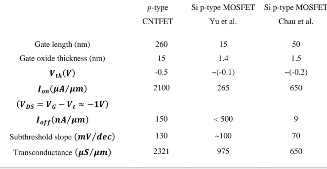
(28) Thèse de Ewa Zbydniewska, Lille 1, 2016. CNTs is very weak and the optical phonon energy is large (. ), that is why the. carrier mobility of nanotubes is high. 45 The carrier scattering by the radial breathing mode (RBM) is important in the low bias regime. The energy of RBM phonons is inversely proportional to the nanotube diameter46 and comparable to the thermal energy of electrons in CNTs with diameters. –. .. Electrons can be accelerated up to the RBM energy thermally and/or by applying source-drain bias of a few. .. The van Hove singularities in the CNTs density of states are finally also responsible for the non-monotonic dependence of the mobility with respect to band filling.42,44,47 By applying the gate potential the band gets filled so the mobility increases because of the reduction of available final (scattered) states. The mobility is then again lowered down when an additional scattering channel opens once the Fermi level reaches a higher-energy 1D subband. The carrier mobility in CNT depends on the diameter quadratically because of the inverse diameter dependence of the effective mass and of the amplitude of the electron– phonon coupling.42 In a CNT, the optical phonons contract and elongate the C–C bond length and lead to a strong modulation of the electronic structure which explains why the optical phonon scattering is very strong in this material. The energy of electrons must be larger than the optical phonon energy to emit an optical phonon. These scattering processes were observed first in metallic nanotubes48,49,50 and later in semiconducting nanotubes.51 In metallic CNTs, the observed current was saturating at about free path, of the order of. –. because of the short optical phonon mean-. , whereas in semiconducting CNTs, a velocity saturation. was observed51 in agreement with earlier theoretical predictions. 51,52. 1.2.3 Performance of carbon nanotube field effect transistors Here, a short discussion about the performance of CNTFETs is given by raising a question whether CNTFETs can replace silicon MOSFETs with respect to the ITRS (International Technology Roadmap for Semiconductors) roadmap.53 In 2002, Wind et al.54 proposed a comparison between top gated CNTFETs and two state-of-the-art silicon MOSFETs. The first type is a 15 nm gate length MOSFET built on bulk Si reported by Yu et al.,55 and the second - a 50 nm gate length device reported by Chau et al.,56 built using siliconon-insulator (SOI) technology. The table 1.1 presents the comparison of transistor performances. 12 © 2016 Tous droits réservés.. doc.univ-lille1.fr.
(29) Thèse de Ewa Zbydniewska, Lille 1, 2016. p-type. Si p-type MOSFET. Si p-type MOSFET. CNTFET. Yu et al.. Chau et al.. Gate length (nm). 260. 15. 50. Gate oxide thickness (nm). 15. 1.4. 1.5. -0.5. ~(-0.1). ~(-0.2). 2100. 265. 650. 150. < 500. 9. Subthreshold slope. 130. ~100. 70. Transconductance. 2321. 975. 650. Table 1.1 Performance comparison of field effect transistors: a 260 nm long top gate p-type CNTFET, a 15 nm bulk Si p-type MOSFET (Yu et al.), and a 50 nm SOI p-type MOSFET (Chau et al.). Adapted from54. The top gate CNTFET prepared by Wind et al. proved to be capable of approximately three to four times higher drive current per unit (. ) width than the Si p-type. MOSFETs at a gate overdrive around 1 V, with approximately two to four times higher transconductance (. ). The comparison is especially impressive since both. the channel length and gate oxide thicknesses are significantly larger for the CNFET than for the silicon devices. Wind et al. assumed further progress can be made in CNTFET device performance via reductions in gate dielectric thickness and/or higher dielectric constant materials, along with reductions in gate length. In addition, a high the cutoff frequency ( of the order of. 57. ). The predicted values of while for MOSFETs it is around. value directly increases for CNTFETs are. .58 Regarding the state of the. art, in 2007, Louarn et al.59 presented direct measured. cutoff frequency for a. nanotube transistor and in year 2008, Zhong et al.60 present a terahertz detection in the time domain using a CNTFET.. 1.3 Nonvolatile memories based on carbon nanotubes The current flowing through a CNT can be gated by single electrons, which is the starting point in making transistors with ultra-low power consumption. Also the perspective is to use individual electrons spin degree of freedom to make quantum bits for use in quantum computers. Further, one of the many CNT applications related with charge sensing and 13 © 2016 Tous droits réservés.. doc.univ-lille1.fr.
(30) Thèse de Ewa Zbydniewska, Lille 1, 2016. controlling the CNT device environment is memory device. The aims at developing nonvolatile memories would be their low power character, as well as a high-frequency operation. At this point in the development of CNT-based applications, this paragraph is devoted to memories based on electrical properties of CNTs. Flash memory (developed from EEPROM - Electrically Erasable Programmable Read Only Memory) is a type of nonvolatile memory that can be electrically erased and reprogrammed. The information in flash memory devices is stored using a network of transistors called cells. Each cell consists of a control gate and a floating gate separated by a thin layer of an insulating oxide. When a voltage is applied to the cell, electrons build up as negative electric charge in the floating gate enabling to hold one bit of information. The pioneering work on logic circuits composed of single-nanotube field-effect transistors was done by A. Bachtold et al.61 The group was studying the nonconventional screening of charge along the one-dimensional nanotubes.. Figure 1.8 (a) AFM image of CNTFET, scale bar is 1 μm. (b) Transfer characteristic of the device measured at room temperature. The arrows are indicating the gate voltage sweep direction and a pronounced hysteresis is observed. (c) Four read/write cycles of the CNT memory. The memory state was read at -1 V, and written with pulses of ±8 V. Adapted from62. M. S. Fuhrer et al.62 presented a non-volatile memory based on semiconductor SWNT with diameter ~ 2.7 nm and length ~ 4.8 μm (Figure 1.8). In this cell, charges are stored by application of a few volts across the silicon oxide between the nanotube and the silicon substrate back-gate. The charge is then detected by threshold shift of the CNTFET. Discrete configurations of charges corresponding to rearrangement of a single or few electrons are then detected, as a result of the high mobility of the nanotube transistor.. 14 © 2016 Tous droits réservés.. doc.univ-lille1.fr.
(31) Thèse de Ewa Zbydniewska, Lille 1, 2016. Figure 1.9 (a) Scheme of the HfAlO/CNTs/HfAlO/Si MOS memory device. (b) High resolution TEM image of CNTs embedded in HfAlO control and tunneling layers. (c) Transfer characteristics of the CNT-based MOS memory devices and the control sample. Adapted from63. Lu et al.63 created HfAlO/CNTs/HfAlO/Si flash memory device using a CNT as the floating gate. The charge-retention characteristics of the device were determined by measuring its capacitance as a function of the gate voltage (Figure 1.9). The memory effect of the structure was mainly attributed to holes, since negative charge (electrons) writing into the CNTs proved more difficult. A long charge retention time (>104 s) was observed. Ganguly et al.64 introduced a nonvolatile memory structure using metal nanocrystals (NCs) as the floating gate of a CNTFET. The gate electrode was used to regulate the charging and discharging of the metal NCs from the channel. Each charged NC imposes an extra local potential on the CNT channel, and hence alters its electrical conduction, with sensitivity down to the detection of single electron levels (Figure 1.10).. Figure 1.10 (a) Cross section illustration of memory device based on CNT. (b-e) Transfer characteristics (b) without NC at T=300 K and (c) with NC at T=300 K, (d) without NC and (e) with NC at T=10 K. Adapted from64. 15 © 2016 Tous droits réservés.. doc.univ-lille1.fr.
(32) Thèse de Ewa Zbydniewska, Lille 1, 2016. References 1. Millman,. J.,. Halkias.,. C.,. C.. Electronic. Devices. &. Circuits.. At. https://archive.org/details/ElectronicDevicesCircuits 2. Dürkop, T. B. M. K. Properties and applications of high-mobility semiconducting. nanotubes. Journal of Physics: Condensed Matter 16, R553 (2004). 3. Avouris, P., Chen, Z. & Perebeinos, V. Carbon-based electronics. Nat Nanotechnol 2, 605–. 615 (2007). 4. Avouris, P. Carbon nanotube electronics. Chemical Physics 281, 429–445 (2002).. 5. Dresselhaus, M. S., Dresselhaus, G., Avouris, P. (Eds.), Carbon Nanotubes. Synthesis,. Structure, Properties, and Applications. Topics in Applied Physics 80, 119-148 (2001) 6. Iijima, S. Helical microtubules of graphitic carbon. Nature 354, 56–58 (1991).. 7. Wang, X. et al. Fabrication of Ultralong and Electrically Uniform Single-Walled Carbon. Nanotubes on Clean Substrates. Nano Lett. 9, 3137–3141 (2009). 8. Svensson, J. Carbon nanotube transistors:nanotube growth, contact properties and novel. devices. PhD thesis, University of Gothenburg, Sweden (2010). 9. Kreupl, F. et al. Carbon nanotubes in interconnect applications. Microelectronic. Engineering 64, 399–408 (2002). 10. Tans, S. J., Verschueren, A. R. M. and Dekker, C. Room-temperature transistor based on a. single carbon nanotube. Nature 393, 49–52 (1998). 11. Appenzeller, J. et al. Field-Modulated Carrier Transport in Carbon Nanotube Transistors.. Phys. Rev. Lett. 89, 126801 (2002). 12. Volder, M. F. L. D., Tawfick, S. H., Baughman, R. H. & Hart, A. J. Carbon Nanotubes:. Present and Future Commercial Applications. Science 339, 535–539 (2013). 13. Dresselhaus, M. S. et al. Carbon Nanotubes: Synthesis, Structure, Properties and. Applications. Springer-Verlag, volume 80 (2001). 14. Zhou, X. Carbon nanotube transistors, sensors, and beyond. PhD thesis, Cornell University. (2008). 15. Charlier, J-Ch., Blase, X., Roche S. Electronic and transport properties of nanotubes.. Reviews of Modern Physics 79, 677 (2007). 16. Van Hove, L. The Occurrence of Singularities in the Elastic Frequency Distribution of a. Crystal. Phys. Rev. 89, 1189. Rev.al. o.. 16 © 2016 Tous droits réservés.. doc.univ-lille1.fr.
(33) Thèse de Ewa Zbydniewska, Lille 1, 2016. 17. Wildoer, J. W. G., Venema, L. C.,. Rinzler, A. G., Smalley, R. E. and Dekker, C.. Electronic structure of atomically resolved carbon nanotubes. Nature 391, 59-62 (1998). 18. Iijima, S., Ichihashi, T. Single-shell carbon nanotubes of 1-nm diameter. Nature,. 363(6430):603 (1993). 19. Thess, A., Lee, R., Nikolaev, P., Dai, H., Petit, P., Robert, J., Xu, C., Lee, Y. H., Kim, S.. G., Rinzler, A. G., Colbert, D. T., Scuseria, G. E., Tombnek, D., Fischer, J. E. and Smalley, R. E. Crystalline ropes of metallic carbon nanotubes. Science, 273(5274):483-7 (1996). 20. Inami N., Mohamed M. A., Shikoh E. and Fujiwara A. Synthesis-condition dependence of. carbon nanotube growth by alcohol catalytic chemical vapor deposition method. Sci. Technol. Adv. Mater. 8, 292 (2007). 21. Ishigami, N. et al. Crystal plane dependent growth of aligned single-walled carbon. nanotubes on sapphire. J. Am. Chem. Soc. 130, 9918–9924 (2008). 22. Banerjee, S., Naha, S. and Puri, I. K. Molecular simulation of the carbon nanotube growth. mode during catalytic synthesis. Applied Physics Letters 92, 233121–233121–3 (2008). 23. Zdrojek, M., Sobieski, J., Duzynska, A., Zbydniewska, E., Strupinski, W., Judek, J.. Synthesis of carbon nanotubes from propane. Chemical Vapor Deposition 21, 94–98 (2015). 24. Baughman, R. H., Zakhidov, A. A. and de Heer, W. A. Carbon nanotubes - the route toward. applications. Science 297, 787–792 (2002). 25. Arnold, M. S., Green, A. A., Hulvat, J. F., Stupp, S. I. and Hersam, M. C. Sorting carbon. nanotubes by electronic structure using density differentiation. Nat. Nanotechol., 1(1):60-65 (2006). 26. http://www.nanointegris.com. 27. Niyogi, S., M. A. Hamon, D. E. Perea, C. B. Kang, B. Zhao, S. K. Pal, A. E. Wyant, M. E.. Itkis, and R. C. Haddon, Ultrasonic Dispersions of Single-Walled Carbon Nanotubes. Journal of Physical Chemistry B 107, 34-8799 (2003). 28. Moore, V. C., Strano, M.S., Haroz, E.H., Hauge R.H., Smalley, R.E., Individually. Suspended Single-Walled Carbon Nanotubes in Various Surfactants. Nano Letters 3, 10 (2003). 29. Bahr, J. L., Mickelson, E. T., Bronikowski, M. J., Smalley, R. E. & Tour, J. M. Dissolution. of small diameter single-wall carbon nanotubes in organic solvents? Chem. Commun. 193– 194 (2001).. 17 © 2016 Tous droits réservés.. doc.univ-lille1.fr.
(34) Thèse de Ewa Zbydniewska, Lille 1, 2016. 30. Koshio, A., Yudasaka, M., Zhang, M. & Iijima, S. A Simple Way to Chemically React. Single-Wall Carbon Nanotubes with Organic Materials Using Ultrasonication. Nano Lett. 1, 361–363 (2001). 31. Tans, S., Vershueren, A., Dekker, C. Room temperature transistor based on a single carbon. nanotube. Nature 393, 49-52 (1998). 32. Chen, Z., Appenzeller, J. Knoch, J., Lin, Y-M & Avouris, P. The role of metal-nanotube. contact in the performance of carbon nanotube field-effect transistors. Nano Lett. 5, 1497– 1502 (2005). 33. Martel, R., Schmidt, T., Shea, H. R., Hertel, T. and Avouris, Ph. Single- and multi-wall. carbon nanotube field-effect transistors. Appl. Phys. Lett. 73, 2447 (1998). 34. Avouris, Ph., Hertel, T., Martel, R., Schmidt, T., Shea, H. R., Walkup, R. E. Carbon. nanotubes: nanomechanics, manipulation, and electronic devices. Appl. Surf. Sci. 141, 201 (1999). 35. Wind, S. J., Appenzeller, J., Martel, R., Derycke, V. and Avouris, Ph. Vertical scaling of. carbon nanotube field-effect transistors using top gate electrodes. Appl. Phys. Lett. 80, 3817 (2002). 36. Keller, D. Nano Field Effect Transistors as basic building blocks for sensing. PhD thesis,. University of Basel, Germany (2007). 37. Martel, R. et al. Ambipolar electrical transport in semiconducting single-wall carbon. nanotubes. Phys. Rev. Lett. 87, 256805 (2001). 38. Heinze, S. et al. Carbon nanotubes as Schottky barrier transistors. Phys. Rev. Lett. 89,. 106801 (2002). 39. Radosavljevic, M., Heinze, S., Tersoff, J. & Avouris, P. Drain voltage scaling in carbon. nanotube transistors. Appl. Phys. Lett. 83, 2435–2437 (2003). 40. Landauer, R. Spatial variation of currents and fields due to localized scatterers in metallic. conduction. IBM J. Res. Dev. 32, 306 (1988). 41 42. Buttiker, M. Symmetry of electrical conduction. IBM J. Res. Dev. 32, 317 (1988). Perebeinos, V., Tersoff, J. & Avouris, P. Electron-phonon interaction and transport in. semiconducting carbon nanotubes. Phys. Rev. Lett. 94, 086802 (2005). 43. Zhou, X., Park, J-Y, Huang, S., Liu, J. & McEuen, P. L. Band structure, phonon scattering,. and the performance limit of single-walled carbon nanotube transistors. Phys. Rev. Lett. 95, 146805 (2005).. 18 © 2016 Tous droits réservés.. doc.univ-lille1.fr.
(35) Thèse de Ewa Zbydniewska, Lille 1, 2016. 44. Durkop, T., Getty, S. A., Cobas, E., & Fuhrer, M. S. Extraordinary mobility in. semiconducting carbon nanotubes. Nano Lett. 4, 35–39 (2004). 45. Wiley: Graphene and Carbon Nanotubes: Ultrafast Optics and Relaxation Dynamics -. Ermin Malic, Andreas Knorr. at <http://eu.wiley.com/WileyCDA/WileyTitle/productCd3527411615.html> 46. Saito, R., Dresselhaus, G., & Dresselhaus, M. S. (eds.) Physical properties of carbon. nanotubes. (Imperial College Press, London, 1998). 47. Perebeinos, V., Tersoff, J. & Avouris, P. Mobility in semiconducting carbon nanotubes at. finite carrier density. Nano Lett. 6, 205–208 (2006). 48. Yao, Z., Kane, C. L. & Dekker, C. High-field electrical transport in single-wall carbon. nanotubes. Phys. Rev. Lett. 84, 2941–2944 (2000). 49. Javey, A. et al. High-field quasiballistic transport in short carbon nanotubes. Phys. Rev.. Lett. 92, 106804 (2004). 50. Park, J. Y. et al. Electron-phonon scattering in metallic single-walled carbon nanotubes.. Nano Lett. 4, 517–520 (2004). 51. Chen, Y.-F. & Fuhrer, M. S. Electric-field-dependent charge-carrier velocity in. semiconducting carbon nanotubes. Phys. Rev. Lett. 95, 236803 (2005). 52. Pennington, G. & Goldsman, N. Semiclassical transport and phonon scattering of electrons. in semiconducting carbon nanotubes. Phys. Rev. B 68, 045426 (2003). 53. The International Technology Roadmap for Semiconductors is a set of documents produced. by a group of semiconductor industry experts. These experts are representative of the sponsoring organisations which include the Semiconductor Industry Associations of the United States, Europe, Japan, South Korea and Taiwan. http://www.itrs.net/home.html 54. Wind, S. J., Appenzeller, J., Martel, R., Derycke, V. & Avouris, P. Vertical scaling of. carbon nanotube field-effect transistors using top gate electrodes. Applied Physics Letters 80, 3817–3819 (2002). 55. B. Yu, Proceedings IEDM 2001, p. 937.. 56. R. Chau, Proceedings IEDM 2001, p. 621.. 57. Burke, P. J. AC performance of nanoelectronics: towards a ballistic THz nanotube. transistor. Solid-State Electronics 48, 1981–1986 (2004). 58. “Low Temperature Implementation of Dopant-Segregated Band-edge Metallic S/D. junctions in Thin-Body SOI p-MOSFETs”, G. Larrieu, E. Dubois, R. Valentin, N. Breil, F.. 19 © 2016 Tous droits réservés.. doc.univ-lille1.fr.
(36) Thèse de Ewa Zbydniewska, Lille 1, 2016. Danneville, G. Dambrine, J.P. Raskin, J.C. Pesant, 2007 IEEE International Electron Devices Meeting, doi: 10.1109/IEDM.2007.4418886 59. Le Louarn A., Kapche F., Bethoux J. M., Happy H., Dambrine G., Derycke V., Chenevier. P., Izard N., Goffman M. F., and Bourgoin J.P. Intrinsic current gain cutoff frequency of 30 GHz with carbon nanotube transistors. Applied Physics Letters, 90(23), 233108 (2007). 60. Zhong Z., Gabor N.M., Sharping J.E., Gaeta A.L., and McEuen P.L.. Terahertz time-. domain measurements of ballistic electron resonance in a single-walled carbon nanotube. Nature Nanotechnology, 3, 201-205 (2008). 61. Bachtold, A. et al., Logic Circuits with Carbon Nanotube Transistors. Science 294, 1317. (2001). 62. Fuhrer, M. S., Kim, B. M., Dürkop, T. & Brintlinger, T. High-Mobility Nanotube. Transistor Memory. Nano Lett. 2, 755–759 (2002). 63. Lu, X. B. & Dai, J. Y. Memory effects of carbon nanotubes as charge storage nodes for. floating gate memory applications. Applied Physics Letters 88, 113104 (2006). 64. Ganguly, U., Kan, E. C. & Zhang, Y. Carbon nanotube-based nonvolatile memory with. charge storage in metal nanocrystals. Applied Physics Letters 87, 043108 (2005).. 20 © 2016 Tous droits réservés.. doc.univ-lille1.fr.
(37) Thèse de Ewa Zbydniewska, Lille 1, 2016. Chapter 2. Semiconductor nanocrystals The history of low-dimensional semiconductor structures began in 1974, when almost simultaneously, IBM1 and Bell Laboratories2 presented the first semiconductor quantum wells. The number of spatial dimensions of the structure is effectively reduced to two as a result of reduced spatial carrier motion in the direction perpendicular to the plane of the quantum well. Further developments in semiconductor nanofabrication technologies allowed producing quantum wires,3 in which the degree of freedom of charge carrier motions has been reduced to one. The total carrier confinement in all three spatial dimensions was obtained in quantum dots (QDs). The first person to use the term quantum dot, related to zerodimensional semiconductor nanocrystal, was Mark Reed4 from Texas Instruments. Initially, QDs have been produced from the quantum wells. The electron confinement in directions parallel to the plane of the quantum well was achieved by applying appropriate voltages to the electrodes disposed in the near vicinity of quantum well.5 In 1981, Alexey Ekimov discovered QDs in a glass matrix6 and then in 1985 NCs were fabricated in the form of colloidal solutions by Louis E. Brus.7 The smallest diameters of first fabricated dots were about. .. QDs attract much attention because they can link the gap between the bulk and molecular levels and lead to broad range of applications e.g. in electronics and optoelectronics. There is also a considerable cognitive aspect associated with the possibility of discovering the meanders of quantum mechanics on a new physical object - an artificial atom.. 2.1 Basics of semiconductor nanocrystals The following paragraph provides a general introduction to the theory of QDs, a short description of quantum confinement in semiconductors, QDs synthesis, and a description of a core-shell QDs. Hereafter the term semiconductor nanocrystals (NCs) and quantum dots will be used interchangeably.. 21 © 2016 Tous droits réservés.. doc.univ-lille1.fr.
(38) Thèse de Ewa Zbydniewska, Lille 1, 2016. 2.1.1 Quantum confinement in semiconductors Three-directional (3D) semiconductors can be classified by their compositiondependent band gap energy (. ), where. is the minimum energy required to excite an. electron from the ground state of the valence band into the vacant conduction band (Figure 2.1a)8, for instance under optical excitation. So, if the energy of an absorbed photon is greater than. , this process leaves a hole in the valence band. The lowest energy state of the created. interacting electron-hole pair, is known as an exciton. The exciton can be annihilated if the electron relaxes back to the valence band and a photon may be emitted in this process, which is called radiative recombination. The exciton has a size defined by its Bohr radius ( which can vary from. ),. to more than. depending on the semiconductor material. If. the size of a nanocrystal is smaller than. , the exciton energy increases, which defines the. transition between the bulk crystal properties and the quantum confinement regime. This leads to absorption and fluorescence spectra which is size-dependent. Figure 2.1b illustrates this effect for quasi-spherical cadmium selenide (CdSe) nanocrystals, showing that the fluorescence and absorption of NCs can be tuned by the size of the nanocrystal. CdSe NCs can be tuned to emit fluorescent light in the full visible spectrum range.. Figure 2.1 Quantum confinement in semiconductors. (a) Schematics of the electronic energy states in a semiconductor showing the transition from nanocrystals and 3D crystals. (b) Absorption and fluorescence spectra of CdSe nanocrystals (AU - arbitrary units). (c) DOS scheme for one band of a semiconductor ,9 structure of 3, 2, 1, and 0 dimensions. Adapted from8. 22 © 2016 Tous droits réservés.. doc.univ-lille1.fr.
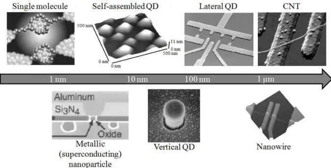
(39) Thèse de Ewa Zbydniewska, Lille 1, 2016. There are several possibilities to confine electronic levels in semiconductors, and various types of NCs exist. Figure 2.2 shows examples of objects from which zerodimensional quantum confinement properties can be observed: single molecules,10 metallic nanoparticles,11 semiconductor self-assembled quantum dots or nanocrystals,12 lateral or vertical dots in semiconductor heterostructures,13 semiconducting nanowires14 and carbon nanotubes.15. Figure 2.2 Examples of different systems with a variety of sizes and aspect ratios behaving as quantum 15 dots. Adapted from. 2.1.2 Quantum dot synthesis The great interest around quantum dots began in 1983, following Louis Brus observation. He was investigating organic redox reactions taking place on the surfaces of photoexcited semiconductors. To do this, he used colloidal semiconductors (in aqueous solution) to obtain higher surface area for the reactions.16 He observed that the band gap was experimentally varying as a function of the particle size. Through this discovery, researchers began to understand that nanocrystals can be highly important for micro and optoelectronics. Nowadays nanocrystals are commonly fabricated as colloids or as epitaxial structures grown on solid crystalline substrates. Epitaxial nanocrystals can be prepared with a wide range of shapes and sizes in regular patterns. The advantage of this method is that nanocrystals can by directly integrated in devices. However, solution phase techniques. 23 © 2016 Tous droits réservés.. doc.univ-lille1.fr.
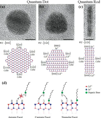
(40) Thèse de Ewa Zbydniewska, Lille 1, 2016. provide exceptional control over size, monodispersity and shape; their low price, in comparison with the epitaxial method, is also one of their advantages. In this work, we used colloidal nanocrystals synthesized from metal organic precursors17 and solvents, as illustrated in Figure 2.3. The metal organic precursors decompose upon heating, and form monomers which allow nucleating the nanocrystals. The synthesis temperature must be high enough to allow for rearrangement and annealing of atoms, but low enough to favor crystal growth. Another critical parameter is the concentration of monomers, leading to two different growth regimes ("defocusing" and “focusing” regimes) from which the size distribution of the grown nanocrystals can be optimized. The great advantage of colloidal synthesis is that large quantities of different types of semiconductor NCs can be fabricated, which is promising for commercial applications.. Figure 2.3 Colloidal nanocrystal synthesis. (a) Schematics of synthesis process. The growth of nanocrystals occurs after the injection of metal and chalcogenide precursors into a hot solvent. (b) Illustration of the control of the nanocrystal size from the growth time. (c) Experimental effective 18 19 bandgap of CdSe nanocrystals as a function of their radius. Adapted from ,. 2.1.3 Core-shell QDs Due to the small particle size, the surface to volume ratio of NCs is relatively high. The atoms on the nanocrystal surface are not bonded completely with the crystal lattice. This way crystalline periodicity is distorted and can form one or more "dangling orbital" sticking out from each atom of the NC surface. Interactions between the NC surface atoms and the surrounding molecules can also significantly affect their optical properties.8 Nanocrystals exhibit in general facets (see Figure 2.4a-c for illustration), each of the facets containing unpassivated orbitals corresponding to surface states.20,21 If the energy level 24 © 2016 Tous droits réservés.. doc.univ-lille1.fr.
(41) Thèse de Ewa Zbydniewska, Lille 1, 2016. of surface states fall within the semiconductor band gap, they can lead to charge carrier trapping at the quantum dot surface. This trapping reduces the overlap between electrons and holes, and favors the probability of nonradiative with respect to radiative relaxation events.. Figure 2.4 An example of surface properties of CdSe nanocrystals. (a), (b) and (c) TEM images of NCs 22 with different shapes (scale bars are 5 nm) together with atomic models. (d) the terminal dangling orbitals on each type of facet. Adapted from8. To enhance the fluorescence of NCs and reduce the influence of surface states, semiconductor nanocrystals can be coated with an insulating inorganic shell. This process passivates the surface bonds, and adds a material acting as an energy barrier around the nanocrystal. The electronic wave-functions of the nanocrystal charge carriers therefore become concentrated at the nanocrystal core, and do not overlap with its surface,23, 24 thus reducing the influence of surface defects onto the fluorescence efficiency. In this work, we used CdSe/ZnS nanocrystals commercially acquired from MKNano, which still exhibit blinking properties (see hereafter).. 25 © 2016 Tous droits réservés.. doc.univ-lille1.fr.
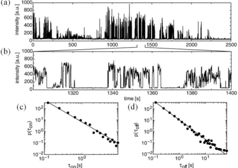
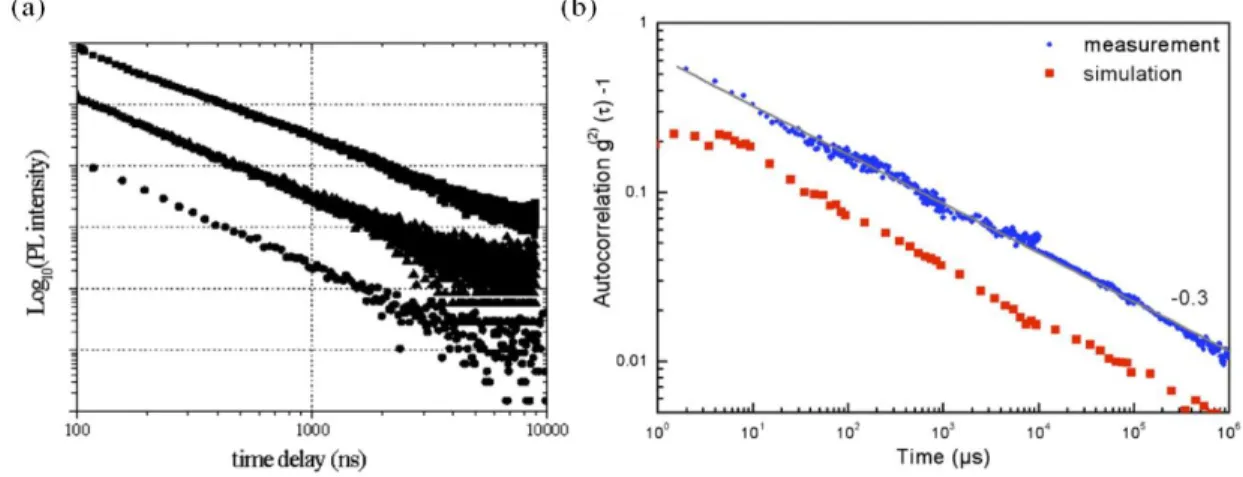
(42) Thèse de Ewa Zbydniewska, Lille 1, 2016. 2.2 Blinking of single QD The phenomenon known as “optical blinking” is a two-level intermittency in which the fluorescence of a quantum dot is observed to be switched on and off as a function of time. Early approaches have attributed optical blinking to the fluctuation of the charge occupation of the NC, in which fluorescence of an electrically neutral quantum dot is switched off in the case of a charged NC.25 This phenomenon is on the one hand extremely puzzling, and on the other hand technologically important while using NCs as light sources. It has therefore become a very active research topic, and has been mostly investigated from optical measurements26,. 27. . In addition, electrical behaviors with on/off states attributed to optical. blinking were experimentally observed.28 We present here below a short overview of the optical and electronic blinking properties colloidal NCs. 2.2.1 Confocal luminescence experiments Time-dependent blinking or luminescence intermittency is illustrated in Figure 2.5. It has been observed on time scales ranging from microseconds to minutes, which fall much above the time scales corresponding from the quantum dynamics of excitons (in the range of picoseconds to nanoseconds).29 Interestingly, blinking effect has been observed on a large variety of nanocrystals, ranging from II–VI (CdSe, CdTe) materials, silicon nanocrystals, selfassembled semiconductor InP quantum dots, and even for color centers in nanodiamonds. 29,30. Figure 2.5 Time resolved luminescence experiments. (a) Luminescence intermittency of a single CdSe/ZnS in polystyrene showing a clear random telegraph pattern. (b) Zoom in on the time trace presented in graph 29 (a). (c-d) Distributions of on- and off-times followed by power-laws Adapted from. 26 © 2016 Tous droits réservés.. doc.univ-lille1.fr.
(43) Thèse de Ewa Zbydniewska, Lille 1, 2016. Nirmal et al.31 have observed for the first time blinking of single CdSe colloids capped with a ZnS shell (and surfactant molecules such as trioctylphosphine oxide) which had been spin-coated onto silicon dioxide substrates. A sequence of active luminescence (on state) and inactive luminescence (off state, no optical emission) equivalent to random telegraph signals has been observed, with on and off state durations ranging from. to several. . The. observed on- and off-time probability distribution ( ) shows, in general, a power-law statistics: f( )∝. −. , with power-law exponents. in the range between 1.1. and 2.2 (the. exponents may vary upon the detection threshold and binning time of the experimental set-up due to the divergence of the power-law).32 The shortest binning times are in usual limited to due to CCD optical detectors (see the examples shown in Figure 2.5), but Verberk et al.33 used an autocorrelation techniques pointing towards blinking times down to the excited state lifetime of. . Figure 2.6 presents two examples of sub-millisecond power-law. dependencies.. Figure 2.6 Power law statistics (a) Time-correlated single-photon counting experiments of NCs ensembles with the detection time of . (b) Autocorrelation function of the luminescence intensity of an 33 29 individual CdS NC followed by power law from 1 s down to ~1μs. Adapted from. The blinking of semiconductor nanocrystals was assigned in early models34 to the photoejection (photoionization), most likely of an electron because of its more extended wave function, thus implying that the NC charged state would be associated with a positive charge. This has been observed experimentally for the first time in 1999 by Krauss and Brus 35 who performed electrostatic force microscopy to detect the electrostatic blinking of the charge state of CdSe nanocrystals at a low time scale (typically of the order of a few minutes) and its switching between a neutral and a positively charged (+e) state. The presence of a charge in the NC efficiently introduces non-radiative Auger processes29 which can predominate over the radiative optical process, and thus quench the NC fluorescence. According to trap models, the 27 © 2016 Tous droits réservés.. doc.univ-lille1.fr.
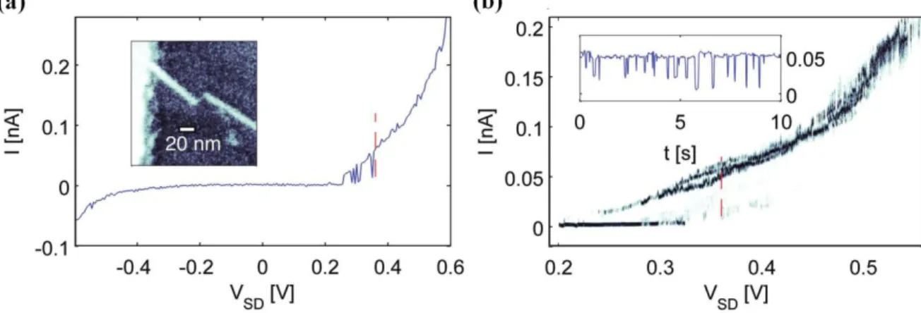
(44) Thèse de Ewa Zbydniewska, Lille 1, 2016. ejected charge tunnels back and forth between the nanocrystal and trap sites giving rise to the observed power-law behaviors. Figure 2.7a presents a schematics of this ‘conventional’ blinking mechanism, more recently referred to as A-type blinking by Galland et al.36 The on and off times correspond to a neutral and a charged nanocrystal, respectively. The on state fluorescence is associated with the radiative recombination of the neutral exciton, characterized by a mono-exponential decay (. –. (see Figure 2.7) with a dynamics in CdSe nanocrystals).37,38,39 The off. state is dominated by a faster and non-radiative process involving a charged exciton. . This. model agrees with the fluorescence behaviors observed in experiments,37,38,40 corresponding either to actual blinking (Figure 2.7c) in which the fluorescence signal is analogous to random telegraph signal, or to flickering, if the two states are averaged during the data acquisition bin times.. Figure 2.7 Blinking behavior of individual NCs. A-type blinking and flickering models. (a) The conventional blinking model, in which and states correspond to a neutral nanocrystal ( ) and a charged nanocrystal ( ), respectively. (b) Scheme of the and photoluminescence decays in a logarithmic representation. The time traces observed for blinking and flickering are shown in (c) and (d). 36 Adapted from. 2.2.2 Electrical intermittency of single QDs Random telegraph signal phenomena have been observed in electrical experiments on single quantum dots, in line with the above mentioned work by Krauss and Brus using electrostatic force microscopy on CdSe NCs. These effects are in general related to trap state 28 © 2016 Tous droits réservés.. doc.univ-lille1.fr.
(45) Thèse de Ewa Zbydniewska, Lille 1, 2016. effects. An electrical current intermittency could be, for instance, detected only in case of single NC (the effect was not observed in ensembles of NCs).41,42 The study of local charging dynamics on the surface of a colloidal nanorod (NR) was presented by Steinberg et al.28 Figure 2.8a shows a typical example of a multistable. curve, taken at temperature. .. During the experiment, current versus time traces were measured at the fixed gate voltage, in analogy with the luminescence experiments.43 An example of observed. trace measured at. is presented in the inset to Figure 2.8b, showing the current multistability.. Figure 2.8 Electrical current switching in single nanorods. (a) Transport characteristics showing the current fluctuations at T= 4.2 K. The dotted red vertical line marks the voltage where the data in the inset to (b) is taken. Inset: AFM image of the NR, connected to the tungsten electrodes. The bright region on the left is the Au electrode. (b) Normalized transport characteristic extracted at each voltage from a long time-domain signal with sampling resolution of . Inset: Time domain signal at 28 (marked by a vertical red dashed line), exhibiting current switching between several levels. Adapted from. Steinberg et al. explained the current fluctuations with charging and discharging dynamics of several surface traps. Such an explanation was quantitatively established in case of bistable current traces (see Figure 2.9a), where the probability for the time spent at the or current state followed an exponential dependence (Figure 2.9c-d). This behavior was then modeled by charging dynamics of a single surface trap.. 29 © 2016 Tous droits réservés.. doc.univ-lille1.fr.
(46) Thèse de Ewa Zbydniewska, Lille 1, 2016. Figure 2.9 Current statistics. (a) characteristics at and . The sampling time is . (b) Corresponding current histogram. (c-d) Probability densities of the high (H) and low (L) 28 current states. Adapted from. 2.3 Electronic properties of coupled QDs and CNTs In the field of electronics, noise is treated as a random fluctuation in an electrical signal, a characteristic of all electronic circuits.44 While noise is generally unwanted, it can be used as an important tool in nanoelectronics. In traditional MOSFETs, the current noise power spectrum at low frequency follows a. law (Figure 2.10a). Generally, the. noise is. understood as the superposition of random events of single-charge trapping and de-trapping from the oxide defects situated close to the semiconductor channel.45,46 In a submicrometer MOSFETs, only a few traps exist, and a discrete switching of the current between two (or more) levels under constant bias conditions can be observed.47 These fluctuations are known as a random telegraph signal (RTS) or random telegraph noise. They have been also observed in systems based on semiconductor nanocrystals28,48 and in CNTFETs.49,50 Such a noise gives rise to a Lorentzian distribution in the current noise power spectrum (Figure 2.10b).. 30 © 2016 Tous droits réservés.. doc.univ-lille1.fr.
Figure
+7
Documents relatifs
