HAL Id: hal-01061361
https://hal.archives-ouvertes.fr/hal-01061361
Submitted on 25 Nov 2016HAL is a multi-disciplinary open access archive for the deposit and dissemination of sci-entific research documents, whether they are pub-lished or not. The documents may come from teaching and research institutions in France or abroad, or from public or private research centers.
L’archive ouverte pluridisciplinaire HAL, est destinée au dépôt et à la diffusion de documents scientifiques de niveau recherche, publiés ou non, émanant des établissements d’enseignement et de recherche français ou étrangers, des laboratoires publics ou privés.
Carriers in Layered 2D Hybrid Perovskites
Jacky Even, Laurent Pedesseau, Claudine Katan
To cite this version:
Jacky Even, Laurent Pedesseau, Claudine Katan. Understanding Quantum Confinement of Charge Carriers in Layered 2D Hybrid Perovskites. ChemPhysChem, Wiley-VCH Verlag, 2014, 15 (17), pp.3733-3741. �10.1002/cphc.201402428�. �hal-01061361�
1 Article
Understanding Quantum Confinement of Charge Carriers in Layered 2D Hybrid Perovskites
Jacky Even,* Laurent Pedesseau and Claudine Katan,*
((Dedicated to Professor Abdou Boucekkine, Professor Slimane Loualiche and Professor Jean-Yves Saillard on the occasion of their retirement.))
Prof. J. Even, Dr. L. Pedesseau Université Européenne de Bretagne INSA FOTON UMR 6082
35708 Rennes, France
E-mail: jacky.even@insa-rennes.fr Dr. C. Katan
CNRS
Institut des Sciences Chimiques de Rennes UMR6226 35042 Rennes, France
E-mail: claudine.katan@univ-rennes1.fr
Keywords: 2D materials, density functional calculations, hybrid perovskites, quantum confinement, semiempirical calculations
Layered Hybrid Organic Perovskites (HOP) structures are a class of low-cost two-dimensional (2D) materials that exhibit outstanding optical properties, related to dielectric and quantum confinement effects. While modeling and understanding of quantum confinement are well developed for conventional semiconductors, such knowledge has still to be gained for 2D HOP. In this work, concepts of effective mass and quantum well are carefully investigated and their applicability to 2D HOP is discussed. For ultrathin layers, the effective mass model fails. Absence of superlattice coupling and importance of non-parabolicity effects prevents the use of simple empirical models based on effective masses and envelope function approximations. We suggest an alternative approach where 2D HOP are treated as composite materials and introduce a first principles approach to band offsets calculations. These findings may also be relevant for other classes of layered 2D functional materials.
2 1. Introduction
Nowadays, there is a growing interest in the development of new low-cost material architectures that could enable superior optical functions and greatly enhanced device performances, and at the same time bypass the current high-efficiency high-cost technologies. In fact, conventional semiconductors achieved great success thanks to well-developed but expensive technologies leading to integrated nanoscale electronics and optoelectronics.[1,2] Numerous optoelectronic applications such as lasers, saturable absorbers, solar cells, are based on complex semiconductor heterostructures, operating at room temperature with electrical or optical carrier injection.[3,4] Layered Hybrid Organic Perovskites (HOP) are a class of solution-processable two-dimensional (2D) materials (Figure 1a,b) that offer great potential for nanophotonics and nanoelectronics.[5-13] These materials exhibit extremely large exciton binding energies due to a large dielectric confinement between the inorganic and organic layers, as well as multiexciton resonances.[14,15] Room temperature excitonic emission leads to enhanced non-linear light emission in microcavities, ascribed to strong electro-optical couplings.[16] However, electrical carrier injection and manufacturing of optoelectronic devices, is still a challenging task. Moreover, the underlying mechanism behind electronic and optical processes remains poorly understood and neither dielectric nor quantum confinement has received the focus and attention it has deserved.
In fact, available theoretical studies either give a general description of the electronic band structure, mostly using density functional theory (DFT),[17,18] or focus on the excitonic coupling using effective mass parameters for the carrier dispersion and abrupt dielectric confinement schemes.[19-23] It happens that 2D HOP are very large and complex systems for typical ab-initio simulations, difficult to precisely handle due to the limitations of the available computational resources. For example, many 2D but also three-dimensional (3D) HOP are lead-based compounds for which the importance of spin-orbit coupling (SOC) on
3
both the band structure and optical properties has recently been evidenced.[18,24] Regarding empirical descriptions of excitonic properties in 2D HOP, all the available studies rely on approaches based on abrupt dielectric interfaces and reduced effective masses for the in-plane motion of the electron-hole pairs.[19-23] Contrarily to the layered perovskites, 3D HOP are easier to address and simulations of many-body effects on monoelectronic states and the electron-hole interaction at the ab-initio level (Bethe-Salpeter Equation) have already been reported.[24-26] It is noteworthy that, following pioneering works,[27–29] 3D HOP such as CH3NH3PbX3 (X = I, Br, Cl) (Figure 1c) have recently emerged as a novel class of low-cost materials for solid-state mesoscopic solar cells.[30,31]
For 2D HOP, resonance energies of Wannier-series excitons have been measured and empirically predicted up to the 4s state.[23] The 2D Wannier exciton model leads to a consistent picture where the exciton Bohr radius exceeds by far the thickness of the inorganic layer where it is confined. Now, given the efficient theoretical treatment of electron-hole pair states with a reduced effective mass, it may appear surprising that effective mass or multiband
k.p approaches, useful to calculate energies of monoelectronic states, have seldom been
implemented for 2D HOP.[22] For their 3D counterparts, it has been shown relevant, including the definition of bulk Bloch functions.[24,25,32] We may underline here that the giant SOC in the conduction bands (CB) of 2D and 3D HOP,[18,24] further leads to the reduction of the multiband k.p Hamiltonians to effective mass approaches. In fact, valence bands (VB) are non-degenerate both with and without SOC and an effective mass approach is well suited. Without SOC, CB is degenerate (triply in a cubic phase) requiring a multiband k.p model. SOC lifts CB’s degeneracy and the ground state split-off CB can be described within the effective mass approach. It is more than likely that effective mass models within a quantum well (QW) heterostructure view of the 2D HOP have been seldom used, because these approaches fail to reproduce correctly the continuous evolution of the electronic band gap from 3D HOP to 2D HOP.[22] Thus, little is known about quantum confinement and the
4
subtle interplay between the organic and inorganic layers in this class of materials, while they are at the heart of their attractive properties.
This work aims at putting in perspective the quantum confinement effect in 2D HOP, with special attention on effective mass models. In section 2.1, we introduce the concept of effective mass and highlight its relationship to envelope functions for heterostructures. Next, we discuss in sequence the intrinsic difficulties related to the applicability of the effective mass model to 2D HOP. We especially show that the concept of effective mass fails because relevant Bloch functions are too different from bulk Bloch functions of each part of the heterostructure. In section 2.6, we suggest an alternative approach where 2D HOP are treated as composite materials and introduce a first principles approach to compute band offsets. The last section is devoted to brief concluding remarks. We stress that our results may also be relevant for other classes of 2D layered functional materials.
2. Results and Discussion
2.1 Effective mass modeling of quantum confinement
The electronic band structure of conventional bulk semiconductors is classically described within the effective mass approximation, which is focusing on a simple parabolic fit of the band dispersion in a vinicity of a given point of the Brillouin zone. Multiband effects can be further investigated using the k.p method to include the coupling between bands and the spin-orbit effect.[1,2] The energy eigenfunctions in a bulk crystal are described as Bloch waves:
𝜓!,𝒌 𝒓 = 𝑒!𝒌.𝒓𝑢
!,𝒌(𝒓), (1)
where 𝑛 is the band index (for example, VB or CB), 𝒓 the position vector, 𝒌 the wavevector and 𝑢!,𝒌(𝒓) the periodic part of the eigenfunction.
The effective mass approximation is widely used for semiconductor microstructures and heterostructures. Quantum confinement effects can be predicted even for thin QW.[33] However, from a purely theoretical point of view, the extension of the mass approximation or
5
A/B between two bulk materials A and B (Figure S1), there is no clear theoretical indication how to connect the solutions on either side of the interface. Semiconductor heterostructures are usually described using the envelope function method.[34,35] The electronic eigenfunctions of the heterostructure are characterized by envelope functions that govern a superposition of a complete basis of periodic functions:
𝜓 𝒓 = !𝐹! 𝒓 𝑈!(𝒓), (2)
where 𝐹!(𝒓) are expected to be slowly varying functions and 𝑈!(𝒓) are periodic and rapidly oscillating functions. In order to further simplify the theoretical approach, the envelope function approximation (EFA) is usually implemented.[34,36] This approximation relies on the assumption that many conventional bulk semiconductors are similar in their chemical nature, that heterostructure’s interfaces are coherent, and that the Bloch functions of the bulk materials at high symmetry points of the Brillouin zone differ only slightly. For a simple heterostructure built from two bulk semiconductors, it is convenient to identify the periodic functions, 𝑈!(𝒓), of the heterostructure with the bulk Bloch functions related to the Brillouin zone center:
𝑈!(𝒓) ≈ 𝑈!,𝟎! (𝒓) ≈ 𝑈
!,𝟎! (𝒓) (3)
This approximation has two main advantages. First, the empirical effective mass or generalized k.p Hamiltonian for the whole heterostructure can be constructed easily by assuming constant parameters for each of the materials building the heterostructure, like the effective masses. Secondly, boundary conditions related to the heterostructure, namely wavefunctions matching and current conservation, are reduced to the envelope functions.[34,35,37] In other words, there is no need to have an explicit knowledge of 𝑈!(𝒓) which contain the atomistic information. For a simple effective mass model in a A/B 2D structure perpendicular to the 𝑧 axis having its interface at 𝑧 = 𝑧!:
6 ! !! !!!!(!) !" !!!! = ! !! !!!!(!) !" !!!! (5)
This model can be successfully applied to treat complex nanostructures such as buried quantum dots (QD) of zinc blende or würtzite type in the k.p approximation including multibands, SOC, inhomogeneous strain and many-body effects.[33,38]
Confinement potentials for the electron or holes have also a clear meaning in the EFA and can be combined to empirical or DFT computed material parameters to calculate the eigenvalues and eigenfunctions of the heterostructure.[39,40] The confinement potentials, 𝑉!"#$, can be derived from known experimental affinities or by simulating explicitely heterostructures to account for atomistic relaxations, charge effects and dielectric confinement related to interfaces. Figure S1 is a schematic representation of a first principles approach to compute the valence band-lineup between two semiconductors A and B.[41,42] The conduction and valence band calculations for the bulk materials are combined with a computation of the DFT potential drop at the A/B interface in a A/B heterostructure. For a complex stack, a many body treatment is beyond reach, but the DFT potential drop at the interface can be efficiently corrected by the self energy (GW) eigenvalues obtained for the bulk valence band states.[43-45] However in a number of situations, the EFA fails to reproduce the experimental results even for coherent interfaces. This may happen when a local symmetry breaking occurs at the interface or an interface-related mixing between bulk eigenstates located at different points of the Brillouin zone, drives the heterostructure electronic states.[35,46-48] Thus, it is necessary to explicitly take into account the periodic part of the bulk Bloch functions. The heterostructure periodic functions 𝑈!(𝒓) may be identified to the bulk Bloch functions of one of the semiconductors. The projection of the bulk Bloch functions of the other semiconductors onto the chosen ones lead to additional contributions to the confinement potentials and Hamiltonian.[35,47-49] However, the envelope function method loses the EFA conceptual simplicity and the computational efforts are comparable to that of empirical atomistic
7
approaches, e.g. tight binding (TB) methods.[49,50] In addition, current conservation expressions can not be easily recast within an effective mass approach.[35] The case of incoherent interfaces like in a relaxed buried semiconductor QD or a complex stack of metal oxide semiconductors can hardly be treated at the envelope function level.[44,51] DFT is a valuable tool in such cases. Effective mass or k.p approaches are still interesting to easily compute various bulk physical quantities like the density of states or the optical dielectric constants. Carrier transport across incoherent interfaces is driven by complex hopping mechanisms related to the specific atomic local structure, interfacial dipoles or dangling bonds. Confinement potentials for the electron or holes may be used to understand qualitatively the confinement effects but, from a purely theoretical point of view, predicting confinement effects on the heterostructure eigenstates by combining these potentials with bulk effective masses is not justified.
2.2. Failure of the empirical effective mass model for 2D HOP using a single inorganic QW
More then a decade ago, Mitzi and coworkers proposed a schematic representation for the 2D HOP, introducing the QW concept for these layered structures.[10] This qualitative picture has been widely used and is based on the assumption that 2D HOP are build from semiconducting inorganic sheets alternating with organic layers having much wider band gaps. This leads to type-I QW heterostructures. In fact, in many cases, the CB of the inorganic layers is expected to lie substantially below that of the organic layers, and the VB of the inorganic layers similarly above that of the organic layers. We may notice that this qualitative discussion was essentially proposed to distinguish between type-I and type-II heterostructures, but no quantitative evaluation of quantum confinement has been performed. If we stay within this picture, the inorganic sheets are described as QW for both electrons and holes with finite potential barriers.
8
Let’s start by considering infinite confinement barriers (infinite length and height) and show that this crude approximation does not work properly to deduce band gaps within the effective mass model. Within this approximation, the band gap energy 𝐸! reads
𝐸! = 𝐸!!!+ 𝐸
!"+ 𝐸!" = 𝐸!!! + ℏ
!!!
!! !!" !, (6)
where 𝐸!!! is the band gap of the bulk reference material, 𝐸
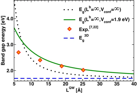
!" and 𝐸!" are the energy of the ground state CB and VB, respectively, calculated for infinite confinement, 𝐿!" is the QW thickness, 𝜇 is the QW reduced mass, 1 𝜇 = 1 𝑚!"!" + 1 𝑚!"!" . The dotted line of Figure 2 reveals the steep slope of band gap energies calculated from expression (6) for small QW thicknesses. When compared to the experimental band gaps reported for (C6H13NH3)2(CH3NH3)l-1PblI3l+1,[22] which has inorganic monolayers (𝑙 = 1), bilayers (𝑙 = 2), trilayers (𝑙 = 3) and tetralayers (𝑙 = 4), it clearly evidences that the increase with decreasing 𝐿!" is by far too sharp (dotted line Figure 2) for reasonable values of 𝐸
!!!and 𝜇, invalidating the infinite confinement barrier approximation. For the interpretation of these experimental results recorded at 5 K[22] (except for the tetralayer recorded at room temperature),[7] Tanaka and coworkers used the effective mass model with finite confinement barriers sketched Figure 3.[22] The reference 3D (l=∞) material (CH3NH3)PbI3 was used for 𝐸!!! with effective masses consistent with those used to evaluate the exciton binding energy, namely the same effective masses for both particles (hole/electron; 𝑚!" = 𝑚!") but different for the QW and barrier (𝑚!" ≠ 𝑚!; Figure 3).[22] However, as quoted by the authors, some arbitrariness remains for the choice of the barrier effective masses. Indeed systematic experimental studies are scarce.[5-13,52,53] This degree of freedom is important because introducing effective mass mismatch is equivalent to adding contributions to the confinement potentials.[34,35] Without any precise indication concerning the barrier material, the effective mass ratio between the QW and the barrier 𝑚!" 𝑚! can be considered as an adjustable parameter which also depends on the nature of the QW/barrier interface. There is no simple formula like (6) for the
9
QW eigenvalues, but the single particle (either electron or hole) ground state energies (𝐸!" and 𝐸!", respectively) can be obtained from the numerical resolution of the following equation given for the CB:[2,54]
𝜂 = tan !!!!" (7)
where 𝜂 = 𝛼𝑚!"!"
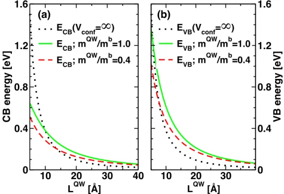
𝑘 𝑚!"! , 𝛼 = 2𝑚!"! 𝑉!"#$,!"− 𝐸!" ℏ!, 𝑘 = 2𝑚!"!"𝐸!" ℏ!. The equation for holes is obtained by replacing CB subscripts by VB. Figure 4 shows both for electron and holes that the energy variations as a function of QW thickness are much steeper for an infinite confinement potential than for a finite one for which the QW band gap is given by:
𝐸! = 𝐸!!!+ 𝐸
!"+ 𝐸!", (8)
where 𝐸!" and 𝐸!" are obtained from equation (7). Despite attempts to adjust the parameters, the model fails to reproduce the experimental band gap of the structure having the thinnest layers (𝑙 = 1). This leads Tanaka and coworkers to the conclusion that the effective mass approximation is not valid for (C6H13NH3)2PbI4.[22] Similar conclusions can be drawn from experimental data recorded at room temperaturethat also include related bromine-based 2D HOP.[7,13]
2.3. Influence of the organic barrier and overestimation of miniband effects in a 2D HOP superlattice
The failure of the model described in section 2.2 is somewhat disappointing because many interesting 2D HOP contain inorganic monolayers (𝑙 = 1). The definition of the quantum object chosen by Tanaka et al.[22] to describe 2D HOP deserves some comments. Most 2D hybrid materials are closer to 2D periodic superlattices rather than to single inorganic QW embedded into infinite organic barriers. It is well-known that electronic miniband formation is the signature of superlattice effects which depend on the barrier thickness 𝐿! and the
10
confinement potential 𝑉!"#$.[2] For a ground state miniband, the energy boundaries are calculated from:
cos 𝑘𝐿!" cosh 𝛼𝐿! +! ! 𝜂 −
!
! sin 𝑘𝐿!" sinh 𝛼𝐿! = ±1. (9) When the thickness 𝐿! of the organic barrier tends to infinity, the miniband effect is predicted to disappear and the case of a single QW (equation (7)) is recovered. Figure 5 shows electron hole ground state miniband energies as a function of barrier thickness for a QW thickness of 6.5 Å. From these results, we may conclude that miniband energies have a sizeable effect on the gap energy of 2D HOP with an organic barrier thickness of ca 10 Å. This corresponds to a superlattice period, 𝐿 = 𝐿!+ 𝐿!"
, of about 16 Å, which is typical for many 2D HOP compounds. For example, for (C5H11NH3)2PbI4 and (pFC6H5C2H4NH3)2PbI4,𝐿 =13 and 16.5 Å, respectively. However, for these hybrids, no energy dispersion parallel to the stacking axis is predicted from DFT calculations.[18] In contrast, for (C2H7IN)2PbI4, the DFT results reveals small dispersions of the band edge states and miniband effects along the direction corresponding to the stacking axis in real space.[55] For this hybrid perovskite, the crystal structure exhibits a slightly smaller stacking parameter (𝐿=12 Å), leading to a weak electronic coupling between the inorganic layers. Moreover, the miniband effect is of the same order of magnitude for VB and CB. This suggests that the balance between the CB and VB confinement potentials proposed in Ref. 22 (Figure 3) may not be the best choice for (C2H7IN)2PbI4. This prompts need for DFT evaluation for each specific hybrid perovskite (vide infra).
In summary, the empirical model with finite confinement potentials and bulk-like effective masses, works quite well for 𝑙 > 1, but fails for ultrathin inorganic QW (𝑙 = 1) and overestimates the miniband effect which is the signature of inorganic interlayer electronic coupling.
11
2.4. Validity of the envelope function formalism and importance of interface effects To understand the origin of this failure, let’s now inspect the validity of EFA and interface effects. In section 2.2, the reduced effective mass, used to predict quantum confinement effects based on equation (6), is derived from the mass of electron-hole correlated motion (excitonic pair states).[22] This assumption is not justified, especially for ultrathin QW. Indeed, quantum confinement and excitonic effects are related to out-of-plane (perpendicular to the stacking axis) and in-plane (within the layers) electronic dispersions and corresponding masses, respectively. Out-of-plane and in-plane dispersions may differ due to a huge interface effect in ultrathin QW. To better understand issues related to interface effects, we can draw a comparison between 2D HOP, conventional semiconductor monolayers embedded into a semiconductor barrier,[56] and ultrathin colloidal nanoplatelets.[57,58] This is sketched Figure 6 so as to highlight periodic bonding along the nearest-neighbor axis for (CH3NH3)PbI3 as well as InAs and CdSe zinc-blende crystals. One has to be careful about the definition of the repeated elementary units as they entail the concept of Bloch function. From the electronic structure point of view, each elementary unit does not simply correspond to a set of atoms, but should also grasp the local environment and bonding of these atoms.[59] Theoretical description of such heterogeneous local environment can hardly rely only on Bloch functions of the bulk material and bulk effective masses. A simple way to incorporate these specific features in an effective mass model is to use local parameters corresponding to an average between the material’s parameters of both bulk compounds. Such approach is closely related to the one used for impurity centers in a periodic crystal studied sixty years ago within the effective mass theory.[49] An effective mass equation can only be derived on the basis of the barrier Bloch functions provided that the impurity produces a “gentle” potential. More recently, atomistic approaches (TB and DFT) were employed to obtain a fine agreement with spectroscopy results and to account for VB degeneracy effects evidenced in colloidal nanoplatelets (NP).[56] NP grow in the zinc-blende phase, with a [001] axis, and are terminated
12
by Cd planes on both sides, which implies a significant non-stoichiometry: a n-monolayer NP consists of n planes of Se and n+1 planes of Cd.[57] This situation is sketched figure 6c. Elementary cells of the bulk zinc-blende structure (figure 6a) are found at the center of a NP with some Cd atoms connected to Se on one side and a ligand on the other side, playing the role of interfaces with the surrounding medium. The ultrathin NP shown figure 6b, with only one Cd atom at the center and nothing related to the bulk repeated unit, is not observed experimentally. However, in very thin NP the influence of interfaces is important and not easily incorporated into multiband k.p or effective mass models using bulk parameters. Moreover, non-parabolicity also manifests itself in the in-plane dispersion showing a strong increase of the CB effective mass with decreasing thicknesses, reaching up to three times the bulk band-edge mass.[58]
2.5. Non-parabolicity of the electronic dispersions in ultrathin 2D HOP
We are now in a position to understand why the case where 𝑙 = 1 in (C6H13NH3)2(CH3NH3)
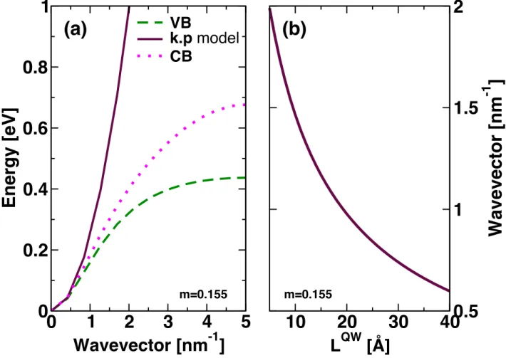
l-1PblI3l+1 should not be treated using parameters derived from (CH3NH3)PbI3, the bulk reference material. By considering a larger effective mass ratio (0.9) and similar confinement potentials (1.9 eV) for electron and hole, the miniband effect occurs for slightly smaller thicknesses than in Figure 5 (Figure S2). However, for monoelectronic states, the effective mass model is still not able to describe the continuous evolution of the electronic band gap from 3D to 2D HOP. This problem is related to another fundamental limitation of these approaches for ultrathin QW. Figure 7a shows the energy dispersion of the VB and CB in the low temperature phase of the 3D bulk reference material, (CH3NH3)PbI3, between the BZ center and the BZ edge.[24] Comparison of the parabolic dispersion deduced from a k.p model using an effective mass of 0.155 and the DFT dispersions evidences strong non-parabolicity for wavevectors larger than 0.5 nm-1. The curvature even changes from positive to negative for wavevectors larger than 1.5 nm-1. From the computed QW wavevector,
13
𝑘 = 2𝑚!"𝐸 ℏ!, for various QW thicknesses shown Figure 7b, one can qualitatively conclude that an effective mass model based on bulk parameters is well suited for tetralayers (𝑙 = 4). Strong non-parabolicity shows off already for trilayers (𝑙 = 3) and bilayers (𝑙 = 2). The specific case where 𝑙 = 1 (monolayers where 𝑘~2 nm-1) is far beyond the area of applicability of the effective mass model. This is consistent with the poor agreement between experimental data and results derived from the effective mass approach reported Figure 2. A rough way to achieve a better fit of the experimental data would be to consider larger effective masses for small QW thicknesses, i.e. effective mass changes with QW thickness as has been implemented for NP.[57,58] Alternatively, one could also increase the size of the Bloch function basis set,[46] use an empirical atomistic TB approach for heterostructures,[46,58] or consider the 2D hybrid crystal as a single composite material.[12,17,18] However, one may seek to keep the description as close as possible to the one that is widespread for conventional semiconductors and this will be addressed in the next section.
2.6. First principles approach to band offsets in 2D HOP
In a conventional semiconductor A/B heterostructure (Figure S1), the precise knowledge of the A and B bulk materials structures is the usual starting point. The difficulty often lies in having access to precise experimental indications on the A/B heterostructure or to build it using empirical or DFT simulation codes. One faces a different problem for describing 2D HOP. The equivalent A/B heterostructure (the 2D HOP) is well known, but the A and B bulk partners are not easily defined. At a first glance, A and B may be defined as the inorganic and organic layers, respectively. We already showed in sections 2.3-2.5 that material A cannot simply be approximated by the bulk (CH3NH3)PbI3 crystal. Moreover, it is not conceptually possible to identify the A and B bulk partners with the inorganic PbI4-2 layer and the sheet of organic cations, respectively, because the Coulomb interactions have a large impact on the
14
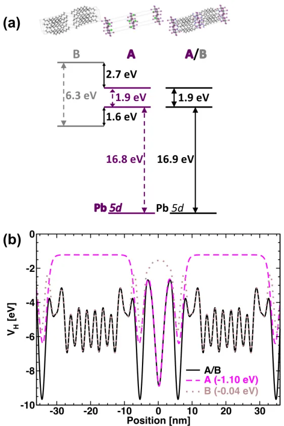
electronic structure of the hybrid material, especially for electronic states located close to the electronic band gap. Here we suggest describing the whole structure as a composite material in a slightly different way. Figure 8a is a schematic representation of the three chemical structures used for such composite approach to compute the valence band-lineup of (C10H21NH3)2PbI4. The A/B structure on the right corresponds to the complete crystallographic structure (orthorhombic phase) reported by Lemmerer and Billing.[63] Structure A corresponds to an inorganic PbI4-2 perovskite layer with additional Na cations (Figure 8a, middle). The latter are located at the position of the nitrogen atom of each C10H21NH3+, so asto mimic the strong Coulomb interactions close to the inorganic layer. We have already demonstrated that such a procedure leads to a good description of the electronic band diagrams of 2D and 3D HOP close to their electronic band gaps.[18,24] Structure B is made from organic neutral molecules, namely C10H21CH3, where nitrogen has been replaced by a carbon atom, thus ensuring electroneutrality and avoiding electron double counting (Figure 8a, left).[64] DFT slab calculations were performed for the A/B, A and B structures. Figure 8b compares the potential profiles of the whole (A/B) 2D HOP crystal to that calculated for each separate piece, structures A and B. By applying a downward energy shift of 1.1 eV to the potential calculated for A (inorganic layers + sodium atom), a perfect match is obtained for the two profiles in the inorganic region. This confirms that the electronic states mainly located in the inorganic layers and at energies close to the electronic band gap are well described by the simplified structure A. Similar potential profiles are also found for A/B and simplified structure B in the region where the organic molecules are located (Figure 8b). To match the two profiles, a small downward shift of 0.04 eV must be applied. This analysis shows that 2D HOP can be considered as composite materials with very weak interactions between the inorganic layers, otherwise such reconstruction of the whole profile by pieces would not have been possible. We may underline that such a procedure requires non-ionic
15
reference materials A and B and that while for A, effective masses match those of A/B, it is not reasonable to deduce effective masses for B on its own.
Besides, comparison of the potential profile of (C10H21NH3)2PbI4 with that calculated for (C5H11NH3)2PbI4 (Figure S3) reveals similar shapes in the inorganic region. This helps to understand why the energy gaps remain almost unchanged for 2D HOP having the same inorganic structure. Variations of the energy gaps are mainly associated to lattice distortions.[12,17,18] These distortions are related to the chemical structure of the organic cations. In this sense, the organic layer has an indirect influence on the energy gap. Moreover, the diagram shown Figure 8a obtained by considering the 2D hybrid as a composite material clearly evidences the type-I nature of the CB and VB band alignment.[60] As for the potential profile (Figure 8b), the CB and the VB of A match those of the real A/B crystal after a downward shift of 1.1 eV. Interestingly, alignment of the Pb 5d orbitals of both structures is obtained by applying the very same offset (Figure 8a). In fact, Pb 5d orbitals are low lying orbitals virtually unaffected by chemical substitution in such HOP and have already been suggested to offer an electronic marker to deduce absolute VB energies.[24] This further confirms the validity of the present approach. The next step is to align VB and CB of B with respect to those of the whole A/B structure (Figure 8a) by applying a 0.04 eV downshift, deduced from the alignment of their respective potential profiles (Figure 8b). This affords the complete band alignment of A and B “bulk like” materials with respect to each other (Figure 8a). It reveals that the confinement potential of holes is large (1.6 eV) as compared to that of conventional semiconductors, but significantly smaller than the one of electrons (2.7eV). This is in contrast with the currently used diagram shown Figure 3.[22]
3. Conclusion
We have thoroughly explored effects of quantum confinement within the context of 2D organic-inorganic hybrid perovskites. The concept of quantum well and approaches based on
16
effective masses and envelope functions have been carefully investigated as they are at the heart of standard models aiming to simulate quantum confinement in heterostructures having a type-I band alignment. It is shown that for such 2D materials, both experimental data and state of the art DFT calculations rule out the applicability of models based on an ultrathin quantum well with finite confinement barriers. In fact, such empirical models predict superlattice effects that are not observed. Moreover, energies of the confined charge carriers lie in a range where strong non-parabolicity occurs for the commonly used reference bulk material, namely (CH3NH3)PbI3 taken for the inorganic QW. In addition, relevant Bloch functions of the real material cannot be properly recovered from the bulk Bloch functions of each material constituting the heterostructure. This prevents the use of standard continuity equation for effective mass transport. We introduce a first principles approach to the calculation of band offsets, based on an alternative view of these 2D HOP in which the layered crystal is treated as a composite material. It allows deriving the proper band alignment, confirming the type-I character and reveals larger confinement potentials for electrons than for holes, in contrast with earlier assumptions. While this procedure remains correct even for ultrathin QW, i.e. 2D HOP with inorganic monolayers, we underline that this model should not be used to investigate effects of quantum confinement in this case. Further development will concern dielectric confinement as both quantum and dielectric confinements are at the origin of the attractive optoelectronic properties of these layered hybrid perovskites. Last, we hope that this work may also be useful and offer guidance for other classes of 2D functional materials.
Experimental Section
For 3D crystal structures, calculations were performed using the DFT implementation available in the ABINIT package,[66] with the GGA-PBE gradient correction for exchange-correlation[67] and relativistic, norm-conserving, separable, dual-space Gaussian- type
17
pseudopotentials of Goedecker, Teter, and Hutter for all atoms.[68] The SIESTA code was used for the simulation of the superlattices at the GGA-PBE level.[69] The electronic wave functions are expanded onto a plane-wave basis set with an energy cutoff of 950 eV. 4 × 4 × 4 and 4 × 4 × 1 Monkhorst−Pack grids were used for reciprocal space integration in 3D and 2D structures, respectively. Calculations were performed with and without SOC.
Acknowledgements
This work was performed using HPC resources from GENCI-CINES/IDRIS grant 2013-c2013096724. The work is supported by Agence Nationale pour la Recherche (PEROCAI project ANR-10-04).
Received: ((will be filled in by the editorial staff)) Revised: ((will be filled in by the editorial staff)) Published online: ((will be filled in by the editorial staff)) [1] E. Kane, Semiconductors and Semimetals, Vol 1, Academic Press, New-York, USA 1966, pp. 75-100.
[2] S. Chuang, Physics of Optoelectronic Devices (Eds: J. W. Goodman), Wiley, New York, USA 1995.
[3] S. Almosni, C. Robert, T. Nguyen Thanh, C. Cornet, A. Létoublon, T. Quinci, C. Levallois, M. Perrin, J. Kuyyalil, L. Pedesseau, A. Balocchi, P. Barate, J. Even, J.M. Jancu, N. Bertru, X. Marie, O. Durand, A. Le Corre, J. Appl. Phys. 2013, 113, 123509.
[4] C. Robert, A. Bondi, T. T. Nguyen, J. Even, C. Cornet, O. Durand, J.P. Burin, J.M. Jancu, W. Guo, A. Letoublon, H. Folliot, S. Boyer-Richard, M. Perrin, N. Chevalier, O. Dehaese, K. Tavernier, S.Loualiche, A. Le Corre, Appl. Phys. Lett. 2011, 98, 251110.
[5] G. C. Papavassiliou, A. P. Patsis, D. J. Lagouvardos, I. B. Koutselas, Synth. Met. 1993,
57, 3889.
[6] D. B. Mitzi, S. Wang, C. A. Field, C. A. Chess, and A. M. Guloy, Science 1995, 267, 1473.
18
[7] B. Koutselas, L .Ducasse, G. C. Papavassiliou, J. Phys.: Condens. Matter 1996, 8, 1217.
[8] G.C. Papavassiliou, Prog. Solid St. Chem., 1997, 25, 125.
[9] C. R. Kagan, D. B. Mitzi, C. D. Dimitrakopoulos, Science 1999, 286, 945. [10] D. B. Mitzi, K. Chondroudis, C.R. Kagan, IBM J. Res. & Dev. 2001, 45, 1. [11] D. B. Mitzi, J. Chem. Soc., Dalton Trans. 2001, 1, 12.
[12] J. L. Knutson, J. D. Martin, D. Mitzi, Inorg. Chem. 2005, 44, 4699.
[13] R. Parashkov, A. Brehier, A. Georgiev, S. Bouchoule, X. Lafosse, J.-S. Lauret, C. T. Nguyen, M. Leroux, E. Deleporte, in Advanced Materials: Research Trends (Eds: L. A. Basbanes), Nova Science Publishers 2007, Chap.12.
[14] X. Hong, T. Ishihara, A. U. Nurmikko, Phys. Rev. B 1992, 45, 6961.
[15] Y. Kato, D. Ichii, K. Ohashi, H. Kunugita, K. Ema, K. Tanaka, T. Takahashi, T. Kondo, Solid State Comm. 2003, 128, 15.
[16] G. Lanty, A. Bréhier, R. Parashkov, J. S. Lauret, E. Deleporte, New J. Phys. 2008, 10 065007.
[17] S. Sourisseau, N. Louvain, W. Bi, N. Mercier, D. Rondeau, F. Boucher, J.-Y. Buzare, C. Legein, Chem. Mater. 2007, 19, 600.
[18] J. Even, L. Pedesseau, M.-A. Dupertuis, J.-M. Jancu, C. Katan, Phys. Rev. B. 2012, 86, 205301.
[19] T. Ishihara, J. Takahashi, T. Goto, Phys. Rev., B, 1990 42, 11099.
[20] E. A. Muljarov, S. G. Tikhodeev, N. A. Gippius, T. Ishihara, Phys. Rev., B, 1995 51, 14370.
[21] K. Tanaka, F. Sano, T.Takahashi, T. Kondo, R. Ito, K. Ema, Solid State Commun., 2002 122, 249.
[22] K. Tanaka, T. Kondo, Sci. Technol. Adv. Mat., 2003 4, 599.
19
[24] J. Even, L. Pedesseau, J. M. Jancu, C. Katan, J. Phys. Chem. Lett. 2013, 4, 2999. [25] J. Even, L. Pedesseau, J. M. Jancu, C. Katan, Phys. Status Solidi RRL. 2014, 8, 31. [26] P. Umari, E. Mosconi, F. De Angelis, Sci. Rep. 2014, 4, 4467.
[27] A. Kojima, K. Teshima, Y. Shirai, T. Miyasaka, J. Am. Chem. Soc. 2009, 131, 6050. [28] M. M. Lee, J. Teuscher, T. Miyasaka, T. N. Murakami, H. J. Snaith, Science 2012, 338, 643.
[29] H.-S. Kim, C.-R. Lee, J.-H. Im, K.-B. Lee, T. Moehl, A. Marchioro, S.-J. Moon, R. Humphry-Baker, J.-H. Yum, J. E. Moser, M. Grätzel, N.-G. Park, Sci. Rep. 2012, 2, 591. [30] J. Burschka, N. Pellet, S. J. Moon, R. Humphry-Baker, P. Gao, M. K. Nazeeruddin, M. Grätzel, Nature 2013, 499, 316.
[31] M. Liu, M. B. Johnston, H. J. Snaith, Nature 2013, 501, 395.
[32] V. Giorgi, J.-I., Fujisawa, H. Segawa, K. Yamashita, J. Phys. Chem. Lett. 2013, 4, 4213.
[33] C. Cornet, A. Schliwa, J. Even, F. Dore, C. Celebi, A. Letoublon, E. Mace, C. Paranthoen, A. Simon, P. M. Koenraad, N. Bertru, D. Bimberg, S.Loualiche, Phys. Rev. B, 2006 74, 035312.
[34] G. Bastard, J.A. Brum, R. Ferreira, Solid State Physics 1991, 44, 229.
[36] EFA is at the basis of the use of the effective mass approximation in single quantum well heterostructures as well as superlattices. It is thus related to the well-known Kronig-Penney model and its extensions allowing different effective masses for the well and the barrier.
[35] M. G. Burt, J. Phys.: Condens. Matter 1992, 4, 6651. [37] D. J. BenDaniel, C. B. Duke, Phys. Rev. 1966, 152, 683. [38] J. Even, Appl. Phys. Lett., 2009 94, 102105.
20
[40] L. Pedesseau, J. Even, A. Bondi, W. Guo, S. Richard, H. Folliot, C. Labbe, C. Cornet, O. Dehaese, A. Le Corre, O. Durand, S. Loualiche, J. Phys. D 2008, 41, 165505.
[41] C. G. Van de Walle, R. M. Martin, Phys. Rev. 1987, 35, 8154. [42] C. G. Van de Walle, R. M. Martin, Phys. Rev. 1989, 39, 1871.
[43] R. Shaltaf, G. M. Rignanese, X. Gonze, F. Giustino, A. Pasquarello, Phys. Rev. Lett. 2008, 100, 186401.
[44] P-Y. Prodhomme, F. Fontaine-Vive, A. Van Der Geest, P. Blaise, J. Even, Appl. Phys.
Lett., 2011 99, 022101.
[45] C. Mitra, B. Lange, C. Freysoldt, J. Neugebauer, Phys. Rev. B, 2011, 84, 193304. [46] S. Boyer-Richard, F. Raouafi, A. Bondi, L. Pedesseau, C. Katan, J. M. Jancu, J. Even,
Appl. Phys. Lett., 2011 98, 251913.
[47] B. A. Foreman, Phys. Rev. B, 1993 48, 4964. [48] B. A. Foreman, Phys. Rev. Lett, 1999 81, 425. [49] J. M. Luttinger, W. Kohn, Phys. Rev., 1955 97, 869.
[50] C. Robert, C. Cornet, P. Turban, T. Nguyen Thanh, M.O. Nestoklon, J. Even, J. M. Jancu, M. Perrin, H. Folliot, T. Rohel, S. Tricot, A. Balocchi, D. Lagarde, X. Marie, N. Bertru, O. Durand and A. Le Corre, Phys. Rev., B, 2012 86, 205316.
[51] C. Bru-Chevallier, A. El Akra, D. Pelloux-Gervais, H. Dumont, B. Canut, N. Chauvin, P. Regreny, M. Gendry, G. Patriarche, J. M. Jancu, J. Even, P. Noe, V. Calvo, B. Salem, J. Nanosci. Nanotechno., 2011 11, 9153.
[52] D. B. Mitzi, C. A. Feild, W. T. A. Harrison, A. M. Guloy, Nature, 1994, 364, 16. [53] Y. Tabuchi, K. Asaia, M. Rikukawa, K. Sanui, K. Ishigure, J. Phys. Chem. Solids, 2000 61, 837.
[54] Formula (7) is derived using a simple well and the continuity equations (4) and (5) for the wave function and its derivative, respectively.
21
[55] L. Pedesseau, J. M. Jancu, A. Rolland, E. Deleporte, C. Katan, J. Even, Opt. Quant.
Electron. 2013, DOI: 10.1007/s11082-013-9823-9
[56] R. Samti, F. Raouafi, M. Chaouach, M. Maaref, A. Sakri, J. Even, J. M. Gerard, J. M. Jancu, Appl. Phys. Lett., 2012 101, 012105.
[57] S. Ithurria, M. D. Tessier, B. Mahler, R. P. S. M. Lobo, B. Dubertret, and A. L. Efros,
Nature Materials, 2011 10, 936.
[58] R. Benchamekh, N. A. Gippius, J. Even, M. O. Nestoklon, J. M. Jancu, S. Ithurria, B. Dubertret, A. L. Efros, P. Voisin, Phys. Rev., B, 2014, 89, 035307.
[59] In the case of InAs, an ultrathin layer containing a single In atom has no straightforward relationship with the bulk material’s elementary cell (Figure 6b). None of the As atom is bonded to two In atoms like in the InAs bulk crystal. The two As atoms bonded to the central In atom are bonded to a Ga on the other side. The local environment is somewhat intermediate between pure InAs and pure GaAs bulk materials. In the case of a larger InAs QW embedded in GaAs, As atoms bonded to In and Ga atoms may be considered as the interfaces between InAs and GaAs (Figure 6c).
[60] Band gaps given Figure 8a and used to align CB are calculated band gap at the DFT level without SOC. In fact, it has been shown that due to error cancellation between manybody and SOC effects, DFT band gaps agree with experiment for lead-based HOP.[24] For alkanes, it has been shown that the absorption onset reduces with increasing alkane carbon chain and the DFT value is in qualitative good agreement with the 7 eV recently reported for n-decane.[61]
[61] E. A. Costner, B. K. Long, C. Navar, S. Jockusch, X. Lei, P. Zimmerman, A. Campion, N. J. Turro, C. G. Willson, J. Phys. Chem. A 2009, 113, 9337.
[62] K. Kikuchi, Y. Takeoka, M. Rikukawa and K. Sanui, Current Appl. Phys. 4, 599 (2004)
22
[64] The potential profile of B bulk-like material remains comparable when removing H+ from the ammonium NH3+ group (Figure S4).
[65] T. Baikie, Y. N. Fang, J. M. Kadro, M. Schreyer, F. X. Wei, S. G. Mhaisalkar, M. Graetzel, T. J. White, J. Mater. Chem. A, 2013, 1, 5628.
[66] X. Gonze, B. Amadon, P. M. Anglade, J. M. Beuken, F. Bottin, P. Boulanger, F. Bruneval, D. Caliste, R. Caracas, M. Cote, et al. Comput. Phys. Commun. 2009, 180, 2582. [67] J. P. Perdew, K. Burke, Phys. Rev. Lett. 1996, 77, 3865.
[68] C. Hartwigsen, S. Goedecker, J. Hutter, Phys. Rev. B 1998, 58, 3641.
[69] J. M. Soler, E. Artacho, J. D.Gale, A. Garcia, J. Junquera, P. Ordejon, D. J. Sanchez-Portal, Phys.: Condens. Matter 2002, 14, 2745.
Figure 1. Overview of the 2D layered crystal structures of a) [pFC6H5C2H4NH3]2PbI4, monoclinic phase;[62] b) (C10H21NH3)2PbI4, orthorhombic phase;[63] and 3D crystal structure of c) CH3NH3PbI3 in its low temperature orthorhombic phase.[65]
23
Figure 2. Band gap energies computed for various QW thicknesses for infinite (dotted line, equation (6)) and finite (straight line, equations (7)-(8)) confinement potentials, using an effective mass of 0.155 and the same confinement potential for both particles (1.9 eV). Diamonds indicate experimental data reported for the 2D HOP (C6H13NH3)2(CH3NH3) l-1PblI3l+1, 𝑙 =1,2,3[22] and 4.[7]
Figure 3. Schematic representation of the effective mass Hamiltonian used to compute energy gaps of the 2D HOP (C6H13NH3)2(CH3NH3)l-1PblI3l+1, 𝑙 =1,2,3 and 4.[22]
5
10
15
20
25
30
35
40
LQW [Å]
2.0
3.0
4.0
Band gap energy [eV]
E
g(L
b=
,V
conf=
)
E
g(L
b=
,V
conf=1.9 eV)
Exp.
[7,22]24
Figure 4. Electron (a) and hole (b) ground state energies as a function of QW thickness for an infinite confinement potential (dotted line), a finite confinement potential, with a mass ratio of 1.0 (straight line) and 0.4 (dashed line). Other parameters are taken from ref. 22.
Figure 5. Electron (a) and hole (b) miniband energies as a function of barrier thickness for a QW thickness of 6.5 Å. Other parameters are taken from ref. 22. The energies for an infinite barrier with infinite (dotted line) and finite (dashed line) confinement potentials are shown for comparison.
10
20
30
40
LQW [Å]0
0.4
0.8
1.2
1.6
CB energy [eV]
ECB(Vconf= ) ECB; mQW/mb=1.0 ECB; mQW/mb=0.410
20
30
LQW [Å]0
0.4
0.8
1.2
1.6
VB energy [eV]
EVB(Vconf= ) EVB; mQW/mb=1.0 EVB; mQW/mb=0.4(a)
(b)
10
20
L
b[Å]
0.2
0.4
0.6
0.8
1
CB energy [eV]
10
20
L
b[Å]
0.7
0.8
0.9
1
VB energy [eV]
(a)
(b)
E
CB(L
b=
,V
conf=
)
E
VB(L
b=
,V
conf=
)
E
CB(L
b=
,V
conf=0.9eV)
E
VB(L
b=
,V
conf=2.9eV)
25
Figure 6. Schematic view of the periodic bonding along the nearest-neighbor axis for a) InAs and CdSe zinc-blende bulk crystals, and (CH3NH3)PbI3 bulk, b) ultrathin layers, c) thin QW with interface layers.
Figure 7. a) Energy dispersion of the VB (dashed line) and CB (dotted line) ground states for the low temperature phase of the 3D bulk reference material (CH3NH3)PbI3. The straight line is the parabolic dispersion obtained when considering an effective mass of 0.155. b) QW wavevector computed for various QW thicknesses using the same effective mass.
(a) (b) (c)
Bulk materials and various choices
of periodic cells 2D QW without a 3D unit cell 2D QW with a 3D unit cell
-In-As-In-As-In-As-In-As-In-As- -Cd-Se-Cd-Se-Cd-Se-Cd-Se-Cd-Se-
-Pb-I-Pb-I-Pb-I-Pb-I-Pb-I-
Ga-As-Ga-As- -As-Ga-As-Ga
Ligand-Cd- -Cd-Ligand
Cation I- -I Cation Cation I- -I- -I Cation Ligand-Cd- -Cd- -Cd-Ligand Ga-As-Ga-As- -As- -As-Ga-As-Ga
0
1
2
3
4
5
Wavevector [nm
-1]
0
0.2
0.4
0.6
0.8
1
Energy [eV]
VB
k.p model
CB
10
20
30
40
L
QW[Å]
0.5
1
1.5
2
Wavevector [nm
-1]
(a)
(b)
m=0.155 m=0.15526
Figure 8. a) Schematic representation of the CB and VB band alignment considering the (C10H21NH3)2PbI4 hybrid 2D HOP (A/B) as a composite structure made of A and B modeled by (Na)2PbI4 and C10H21CH3, respectively. b) Computed potential profiles for the real 2D material (A/B, straight line) and A (dashed line) and B (dotted line) bulk-like materials. Band alignment and match of potential profiles of A/B are obtained thanks to downward shifts of the data computed for A and B amounting to 1.1 and 0.04 eV, respectively. Alignment of Pb 5d orbitals between A/B and A also require a 1.1 eV shift.
(a)
6.3$eV$
1.9$eV$
1.6$eV$
2.7$eV$
16.8$eV$
1.9$eV$
16.9$eV$
Pb$5d#
/
B$
-30 -20 -10 0 10 20 30 Position [nm] -10 -8 -6 -4 -2 0 V H [eV] A/B A (-1.10 eV) B (-0.04 eV)(b)
27
Keyword: Hybrid perovskites, quantum well, quantum confinement, photovoltaic, 2D materials
Jacky Even,* Laurent Pedesseau and Claudine Katan,*
Quantum confinement of charge carriers in 2D hybrid perovskites is investigated, starting with the concepts of effective mass and quantum well. For ultrathin layers, the effective mass model fails. An alternative approach where these perovskites are treated as composite materials is suggested including band offsets calculations.
![Figure 1. Overview of the 2D layered crystal structures of a) [pFC 6 H 5 C 2 H 4 NH 3 ] 2 PbI 4 , monoclinic phase; [62] b) (C 10 H 21 NH 3 ) 2 PbI 4 , orthorhombic phase; [63] and 3D crystal structure of c) CH 3 NH 3 PbI 3 in its low temperature o](https://thumb-eu.123doks.com/thumbv2/123doknet/11621960.304559/23.892.282.613.558.975/figure-overview-layered-structures-monoclinic-orthorhombic-structure-temperature.webp)