HAL Id: hal-01110463
https://hal.archives-ouvertes.fr/hal-01110463
Submitted on 28 Jan 2015
HAL is a multi-disciplinary open access
archive for the deposit and dissemination of
sci-entific research documents, whether they are
pub-lished or not. The documents may come from
teaching and research institutions in France or
abroad, or from public or private research centers.
L’archive ouverte pluridisciplinaire HAL, est
destinée au dépôt et à la diffusion de documents
scientifiques de niveau recherche, publiés ou non,
émanant des établissements d’enseignement et de
recherche français ou étrangers, des laboratoires
publics ou privés.
Cryptographically secure shields
Jean-Michel Cioranesco, Jean-Luc Danger, Tarik Graba, Sylvain Guilley, Yves
Mathieu, David Naccache, Xuan Thuy Ngo
To cite this version:
Jean-Michel Cioranesco, Jean-Luc Danger, Tarik Graba, Sylvain Guilley, Yves Mathieu, et al..
Cryp-tographically secure shields. HOST 2014 - IEEE International Symposium on Hardware-Oriented
Security and Trust, May 2014, Washington, United States. pp.25 - 31, �10.1109/HST.2014.6855563�.
�hal-01110463�
Cryptographically Secure Shields
Jean-Michel CIORANESCO
1, Jean-Luc DANGER
2,3, Tarik GRABA
2, Sylvain GUILLEY
2,3,
Yves MATHIEU
2, David NACCACHE
1,4and Xuan Thuy NGO
2,†1Sorbonne Universit´es – Universit´e Paris II, 12 place du Panth´eon, 75 231, Paris Cedex 05, France.
2Institut MINES-TELECOM, TELECOM-ParisTech, CNRS LTCI (UMR 5141),
46 rue Barrault, 75 634 Paris Cedex 13, Franceand 37/39 rue Dareau, 75 014 Paris, France. {danger, graba, guilley, mathieu, xngo}@telecom-paristech.fr
3Secure-IC S.A.S., 37/39 rue Dareau, 75 014 Paris, Franceand 80 avenue des Buttes de Co¨esmes, 35 700 Rennes, France.
{jean-luc.danger, sylvain.guilley}@secure-ic.com
4Ecole normale sup´erieure, D´epartement d’informatique, 45 rue d’Ulm, 75 230, Paris Cedex 05, France.´
†Corresponding author.
Abstract—Probing attacks are serious threats on integrated circuits. Security products often include a protective layer called shield that acts like a digital fence. In this article, we demonstrate a new shield structure that is cryptographically secure. This shield is based on the newly proposed SIMON lightweight block cipher and independent mesh lines to ensure the security against probing attacks of the hardware located behind the shield. Such structure can be proven secure against state-of-the-art invasive attacks. For the first time in the open literature, we describe a chip designed with a digital shield, and give an extensive report of its cost, in terms of power, metal layer(s) to sacrifice and of logic (including the logic to connect it to the CPU). Also, we explain how “Through Silicon Vias” (TSV) technology can be used for the protection against both frontside and backside probing.
Index Terms—Cryptographically secure shield, SIMON block cipher, Focused Ion Beam (FIB), Through Silicon Vias (TSV).
I. INTRODUCTION
Nowadays, hardware trust and security play a important role because integrated circuits (IC) are present in many critical infrastructures for sensitive markets like finance, ID, health, military affairs, etc. Many cryptographic intellectual property blocks (IPs) are integrated to assure the security of ICs. But, these cryptographic IPs can themselves be the target of attacks. Using a probing station, attackers can read data within the circuit, and in particular extract cryptographic keys, hence breaking the IC security (Fig. 1). To thwart this attack, a metallic shield can be added. It is a mesh of metal lines on the top-most metal layer(s) of the IC, that prevents an adversary from reading (and writing) via a probing attack. However, with the progress in attack techniques, the shield protection can still be bypassed if improperly designed. For instance, with a tool called Focused Ion Beam (FIB), attackers can draw artificial pads that conduct directly into the inner parts of the circuit, hence allowing the attacker to spy sensitive signals or secret data (such as keys). Therefore, counter-measures for this kind of attack on the shield are needed.
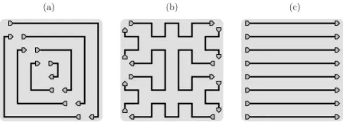
Actually, we can classify the shields in two categories: either passive or active. Passive shielding consists in an analogue integrity check of the mesh. For instance, in [15], P. Laackmann and H. Taddiken present an analog passive shield based on a analog transmitter, an analog receiver, a drive and an evaluation device. The shield is associated with a capacitive measurement method to evaluate it. However, some alterations of the mesh can be undetected, if they are small or surgically-accurate enough to keep the mesh capacitance within acceptable bounds. Hence, digital (active) shielding aims at mitigating this problem. It consists in injecting ran-dom sequences of bits in the mesh, and subsequently in checking whether they arrive unaltered after their journey. An illustration is given in Fig. 2. Such structures exist for the protection of both devices (e.g., FIPS-140 compliant security appliances [16]) and ICs. In this article, we focus on lines meshes suitable for ICs, that use only one metal layer, since they are really favored by the industry; using more than one metal layer is considered prohibitively expensive. For active shields, we can find some ideas of architectures in [2], [14], [13]. Let us call them shield #1, #2 and #3. Shield #1 consists in sending a “predetermined test data” into a small number of equipotentialsin the shield. Flylogic employees defeated this shield by identifying the equipotentials1 in the circuit [20]: they found four of them, which they shorted together in order to make an opening in the shield, thanks to a FIB. Shields #2 and #3 consist in lines that carry the successive values of a linear feedback shift register (see shield #3 in Fig. 2(a)). They are thus also easy to bypass: the value of all the lines can be guessed by solving a system of linear equations. So,
1Notice that the identification of equipotential lines in the circuit does
not require a systematic test-and-trial probing. A technique called “voltage contrast” [18] is able to represent lines of different potential with different shades of gray. So, equipotential lines are those lines that constantly (in time) share the same color.
Fig. 1. Line probing, the basics of a probing attack (courtesy of [23])
(a) (b) (c)
Fig. 2. Some mesh structures for n= 8 lines
in practice, these shields (and in general all the active shields of the state-of-the-art) manage to make probing attacks more difficult, but not impossible. Recently, a new active shield structure (based on a maze, called random active shield) has been proposed [5], [9], [4]. This method achieves intricate spaghetti routing of a dense mesh of wires hence making the geometry of the shield difficult to recognize. However, the large scale generation of such a structure is admittedly complex (see Fig. 2(b)). Moreover, the solution [5] can require several topmost metal layers for the creation of mesh wires: in a compact IC, this makes the routing of the legacy hardware to be protected (below the shield) very challenging. Last but not least, these articles do neither detail the nature of the random numbers, nor the actual cost (i.e., area, power) of the solution. In this article, we present a new shield structure that does not have the limitations of the state-of-the-art:
1) It resists rerouting attacks by FIB because there are no two identical lines: all the wires of the shield carry a different information;
2) The data sent over the shield lines are unpredictable, because they are the output of a block cipher operated in CBC mode;
3) The layout of the mesh is trivial: it simply consists in parallel lines, of minimal width and minimal spacing, as depicted in Fig. 2(c). The input/output ports of our mesh are positioned with a regular spacing on two faces (left and right), which eases their connexion. Notice that the term “mesh” is no longer suited for our shield, since the lines are not entangled. Nevertheless, we keep this term for consistency with previous structures.
4) Only the topmost metal layer is required.
Of course, we insist that passive and active shields do not protect against circuit reverse-engineering by delayering [21]. But they protect against dynamic attacks that consist in
recov-ering sensitive data that are used plain within the chip after its boot, such as keys that are stored decrypted in a non-volatile memory and used in clear during nominal execution.
This article is structured as follows. The cryptographically secure shield is presented in Sec. II. The test and performance of this shield is shown in Sec. III. A methodology for preventing backside attacks (3D circuits) is given in Sec. IV. We finish with some conclusions and future works in Sec. V.
II. CRYPTOGRAPHICALLYSECURESHIELD
A. Rationale
As observed above, the current active shields, presented in Sec. I, cannot assure the ICs security. Attackers can attack these shields thanks to the FIB technique. The principle of this attack is to open some lines, then short-circuit those which are equipotential, thereby creating unprotected areas on the circuit [5], with a shield connectivity unaltered. Alternatively, even if each line carries different data, an attack still exists: indeed, in the case where the value of one line at one clock cycle can be deduced from the value of other lines at the previous clock cycle(s), then a logic analyser can generate on-the-fly the missing signal even if the “targetted” line has been disconnected by FIB to allow for probing beneath it.
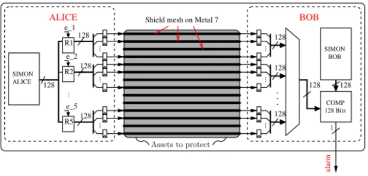
To mitigate these problems, our active shield uses a block cipher in Cipher Block Chaining (CBC) mode to generate random numbers to be sent in the independent shield mesh lines. A priori, any block cipher is suitable, as long as it is cryptographically secure. But, for the compactness of implementation, the best choice is a lightweight block cipher. We leverage on the newly proposed SIMON block cipher [1], that is shown to achieve better time/area tradeoff than other ex-isting lightweight block ciphers (such as TWINE, PRESENT, PICCOLO, KATAN, KLEIN, for instance). Figure 3 shows our shield’s structure (note that both Alice and Bob are located behind the shield mesh). It is composed of three parts:
• ALICE (transmitter), which embeds a SIMON block to
generate128 random bits.
• BOB (receiver), which also embeds a SIMON block and,
in addition, has a128 bits comparator.
• Shield mesh, which is composed of n lines on the
last metal layer. It is used as a communication channel between ALICE and BOB, and achieves the anti-tamper protection of the integrated circuit located below it. The rationale of our shield relies on a simple on-chip unidirectional encrypted communication through the mesh. The two SIMON blocks (belonging to Alice and Bob) share the same key, the same initialization vector (IV), and are operated at the same rate. Therefore they perform the same computation to generate 128 random bits after each cipher computation (128 bits of ciphertext). The shield mesh is made up of n > 128 lines; Thus, Alice sends to Bob its 128 bits through the first, second, etc. packet of 128 bit lines (called R1, R2, etc. in Fig. 3). Enable signals e 1, e 2, etc. allow for such dispatching. If the exchanged128 random bits match, we can deduce that the shield has probably not been altered. The
... ... ... ... ... ... . . . SIMON BOB SIMON ALICE
Shield mesh on Metal 7
128 alarm COMP 128 128 128 e_1 128 128 128 e_2 e_5 128 ALICE BOB 128 Bits R5 R2 R1 128 Assets to protect ... 1
Fig. 3. Unoptimized cryptographically secure shield
alarm signal (output of the comparator) is kept is to low value “0”. Indeed, an attacker can guess the value of each line with
1/2 probability. However, after m exchanges between ALICE
and BOB, the probability of an undetected attack is lowered to 1/2m, because the attacker has no a priori information: he
can at best make independent guesses at random. So, within a short time span, any shield opening or forging (i.e., rerouting) will be detected. Otherwise, when the two 128 random bits sequences differ, the alarm signal is asserted to “1”, to indicate that there is a problem with the shield lines.
In Fig. 3, two different instances of SIMON are used to separate properly ALICE (left) from BOB (right). This separation is meant to minimize the routing of the active shield logic on the circuit. It is routed using only with the topmost metal layer (M7 in our case). Thereby all metal layers between M1 to M6 are free for routing of the remaining parts of the circuit beneath the mesh. This facilitates the placement and routing of the final circuit, because the shield can be inserted once the place and route of all the other blocks is done.
This shield presents the following interesting properties:
• No deterministic sequence. The bit sequences exchanged
in the shield’s lines are the cipher results of SIMON so there is no reuse of the random bits because ciphertexts change after each encryption. To predict these bits, an at-tacker must first cryptanalyze SIMON in order to extract its cipher key k. Indeed, if the block cipher operated in CBC is considered ideal, the next ciphertext cannot be guessed from the previous ones [17, Chap. 7.2.2.]. For a more accurate discussion about security, please refer to Sec. II-B.
• Independant lines. Each line of the shield carries one bit of cipher message. So the attack by FIB cannot bypass more than one line. This greatly reduces, not to say disables, the scope of the attack.
• Low complexity. A lightweight cryptoprocessor (e.g.,
SI-MON) suffices. Besides, our method is very low cost in terms of entropy. The only needed randomness is the key and the IV.
B. Risk of Side-Channel Analysis, and Mitigation
Actually, let apart cryptanalysis, another way of extracting the cryptographic key of SIMON is via side-channel analysis.
S1 S8 S2 Right (R) Left (L) k 64 64 ∧
Fig. 4. Last round of SIMON, where L||R is the ciphertext
However, this attack usually requires the knowledge of either the plaintext or the the ciphertext. In the proposed mode of operation (See forthcoming Fig. 6), only the ciphertext is outputted. Of course, it is hardly feasible to record with a prober station the full 128 bits of the ciphertext, but only a few bits of it. However, a side-channel attack requires a few probes to test of a few bits of the key. One round of SIMON is depicted in Fig. 4. The ciphertext is the concatenation of the two registers L and R, the last round key is denoted k, S1, S8 and S2 are circular left shifts, and
∧ is a Boolean AND. In the Hamming distance leakage model, the leakage function that discloses the bit i∈J0, 63K of k is:
L[i]⊕ k[i] ⊕ R[i − 2] ⊕ (R[i − 8] ∧ R[i − 1])
| {z } initial value ⊕ R[i] |{z} final value .
So,5 probes are needed to extract 1 bit of the key.
Recall the attacker cannot probe directly the key bits (that are located below the shield mesh), but the ciphertext. Though difficult, such setup (probing a5 ciphertext lines for each bit of the key) would not deter a determined attacker. So, a protection of SIMON against side-channel attacks might be necessary. A low-cost countermeasure has been invented and presented by Bhasin et al. [3]. It is shown to increase the area of SIMON by a factor of 67%.
C. Trading SIMON for AES
The SIMON block cipher has been published recently on the IACR ePrint archive [1], a non-peer-reviewed repository of scientific articles. Therefore, it has been less scrutinized than other block ciphers, such as the AES. We discuss in this paragraph the impact of trading SIMON for AES. Obviously, AES-128 is sufficient: as recalled in Sec. II-B, the setup of a side-channel attack on the cryptographic block cipher that feeds the shield mesh is challenging, experimentally speaking. Now, as speed is neither is requirement, one can resort to low-area AES implementations. For instance, it is shown in [8] how to design an extremely compact AES. The cost is 222 CLBs (compound logic block) and 3 block RAMs, which is indeed more costly in terms of silicon area than SIMON. Still, as advocated in [10], AES is one of the most compact block cipher amongst the ones that were proposed before SIMON.
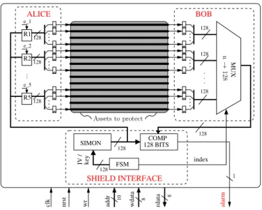
.. . .. . .. . ... .. . .. . MUX . . .
SIMON 128 BITSCOMP FSM
BOB
nrst
clk wr addr wdata rdata
8 8 10 ALICE alarm R1 R2 R5 128 128 128 128 128 128 index 128 e_1 e_2 e_5 128 SHIELD INTERFACE 128 key IV / n → 12 8 Assets to protect ... 1
Fig. 5. Optimized cryptographically secure shield
D. Structure
This section describes the logic path of the cryptographic shield. We actually describe an optimized structure which is functionally equivalent to the one presented in Fig. 3. Its function is presented in Fig. 52. It is composed of three blocks: • ALICE block: composed only of registers and buffers, to amplify the signals before they travel along the capacitive (since long) lines of the mesh.
• BOB block: composed of buffers and one n bit→ 128 bit multiplexer.
• SHIELD INTERFACE: composed of a 128 bit SIMON
block, one 128 bits comparator, and a Finite-State Ma-chine (FSM). The role of the FSM is to handle the connexion with the CPU: the “shield”, seen as an IP, is a slave on the system bus.
The operation of our shield is as follows. We assume that the SIMON block is already keyed, i.e., its cryptographic key k of 128 bits is programmed. Typically, the choice for the key has been done during an enrollment phase (thanks to a privileged “Set key” command). At every power-up, the system chooses a random IV, that is sent to the SIMON block using the “Set IV” command. This mitigates the risk of replay attacks. Then, the SIMON module is operated in CBC mode with the subsequent plaintexts being equal to “0”. As illustrated in Fig. 6, this generates a stream of ciphertexts3. The128-bit
ciphertexts are sent on the wires at position[index, index+127] of the mesh, where index∈ [0, dn/128e−1] is a cyclic counter generated by the FSM.
We recall that the active shield of Sec. II-A had three separated parts to minimize the use of routing resources on
2Figure 5 represents each component in a separated area, whereas in the
actual layout, all the logic (including that driving the shield) is located behind the shield mesh.
3In such a mode, where the IV is arbitrary but the plaintexts are all null,
CBC, CFB and OFB modes of operation generate the same ciphertexts.
“0” “0” “0” “0” 128 128 128 128 IV SIMON k stream[2] SIMON k stream[⌈n/128⌉ − 1] SIMON k stream[0] SIMON k stream[1]
Fig. 6. Mode of operation of the SIMON block (keyed with k), for the
generation of the random data stream flowing through the mesh lines TABLE I
APIOF OUR CRYPTOGRAPHIC ACTIVE SHIELD
Instructions Function description
Set key Write cryptographic key to SIMON block of the shield
Set IV Write the Initialization Vector to SIMON block
Enable/Disable Enable or disable shield block
Get status Read alarm register (5 bits) of the shield
Set freq Configure clock frequency Fclkof the shield
lower metal layers, so as to avoid routing problems for the final circuit. But we have experienced (See Sec. III) that the new “optimized” shield structure can be routed automatically without congestion problem.
E. Connexion to the System-on-Chip
We communicate and control our shield via a simple Ap-plication Programming Interface (API). Table I presents all the instructions it offers. It allows to write (or change) the cipher key k and the IV of SIMON. The shield can be enabled or disabled (when non-critical operations are carried out). Additionally, we can read the alarm register which contains the comparison values of each packet of 128 bits, hence identifying the location of the modifications on the shield (if any). For example, the shield mesh of our circuit has 640 lines which are divided into 5 packets of 128 lines; thus our alarm status register has 5 bit. There are pros and cons to the dedicated hardware alarm wire versus the “Get status” command. The alarm allows to raise a timely interruption to the CPU. However, it is very exposed, because if it is cut, the shield is physically disconnected from the CPU. On the contrary, the software status bits will be checked on coarser time intervals. But they are more resilient to hardware alteration because they are multiple (5 = 640/128 flip-flops in our case), which complicates their disconnection. Eventually, the shield clock frequency Fclkcan be configured via the API
to reduce the power consumption. This topic will be elaborated on in Sec. III-C.
III. TESTCHIP ANDPERFORMANCES A. Layout Level
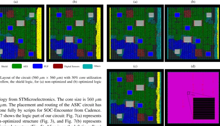
To evaluate the proposed shield, we created an ASIC which is composed of 8 IPs (one shield, plus one AES, one PUF, two digital sensors, etc.) using CMOS065, the CMOS65 nm
(a) (b)
Digital Sensors
Shield AES PUF Others
Fig. 7. Layout of the circuit (560 µm × 560 µm) with 30% core utilization rate. In yellow, the shield logic, for (a) non-optimized and (b) optimized logic
technology from STMicroelectronics. The core size is560 µm × 560 µm. The placement and routing of the ASIC circuit has been done fully by scripts for SOC-Encounter from Cadence. Figure 7 shows the logic part of our circuit: Fig. 7(a) represents the non-optimized structure (Fig. 3), and Fig. 7(b) represents the optimized structure (Fig. 5). Alice is on the left (in yellow) and Bob on the right (in yellow). In the optimized structure, the SHIELD INTERFACE is placed along with Bob. Overall, it can be seen that the optimized structure is smaller than the non-optimized one (as expected). The placement of Alice and Bob has been constrained by a createFence specification of Cadence SOC-Encounter, that allows to confine Verilog modules in a rectangle. We also notice that the shield logic takes a small area in the circuit for both layouts.
Figure 8(a,b,c) show the size of each shield part correspond-ing to the optimized structure (Fig. 7(b)). Alice (Fig. 8(a)) is the emitter, made up of128 registers with enable and 5× 128 buffers to drive the lines of the mesh. Bob (Fig. 8(b)) is the receiver, made up of 5× 128 buffers, a multiplexer to choose 128 bits amongst the 640 (5 → 1), and finally 128 registers. For both Alice and Bob, the buffers are placed at regular locations by a script. The shield interface block is in Fig. 8(c). Finally, the shield mesh lines are in Fig. 8(d) in violet (color of M7). The dense parallel lines cover the full circuit area to protect all IPs inside the circuit, including the shield logic.
Figure 9 shows the placement and routing of Alice buffers (on the left), Bob buffers (on the right), and the shield mesh creation. The buffers are placed vertically by packet of 3. Then parallel lines (shield mesh) on top-most layer (M7 in violet color) are drawn from Alice buffers to Bob buffers with almost minimal width (0.4 µm) and minimal spacing (0.4 µm). We notice that the smallest probe tips available on the market have a diameter of 0.2 µm [6], [7]. So, in theory, they could probe through our shield. However, their diameter leaves only 100 nm on each side of the shield, which makes the probing fairly chancy and a short-circuit highly probable. In the case it is expected that an attacker is likely to use such sophisticated probe tips, a two-layer shield (e.g., by instantiating another
(a) (b)
(c) (d)
zoom
Fig. 8. Shield logic part (detail of Fig. 7(b)) in yellow. (a) ALICE, (b) BOB, (c) SHIELD INTERFACE, (d) shield mesh lines in M7 (with zoom)
(a) (b)
Fig. 9. (a) Alice & (b) Bob buffers placement and routing independent shield, with a mesh rotated by90 degrees) might still increase the complexity of a probing attack. In addition, in our 65 nm process (said: 7m4x0y2z, meaning that the spacing for M1 to M5 is the same, smaller than that of M6 and M7), the spacing for M5 is only 0.1 µm. This is four times smaller than for M6 or M7. Thus, a shield in M5 would deny any attack. In any case, metal densities design rules are fulfilled. We emphasize that only Alice and Bob buffers are placed and routed by scripts. All others placement and routing are done by automatic SOC-Encounter tools.
B. Area
To create the shield, the top-most metal layer (M7 in our case study) must be sacrificed. However, this is the minimal cost for all shield structures. Table II gives an overview of the size and surface area occupied by some IPs in our ASIC circuit (namely the shield and the AES). The shield logic needs4001 cells. It is still small compared to other IPs in our circuit (for example, the AES needs10292 cells). The shield takes 6.18 %
of the final circuit (Figure 8). For a circuit of x µm× y µm, the cell area of the shield Sshield= SAlice+ SBob+ Sinterface can
be estimated as:
SAlice = 3941.6× y ÷ 560 µm2 ,
SBob = SAlice+ SMultiplexer≈ 4854.2 × y ÷ 560 µm2 ,
Sinterface = 10571.6 µm2 .
In these equations, we make the rough approximation that the size of the multiplexer grows (quasi)linearly with the number of inputs. So with a larger circuit, the percentage of area occupied by the shield decreases considerably.
TABLE II
SIZE AND AREA OCCUPIED BY SOMEIPS
Instance Cells Total Percentage
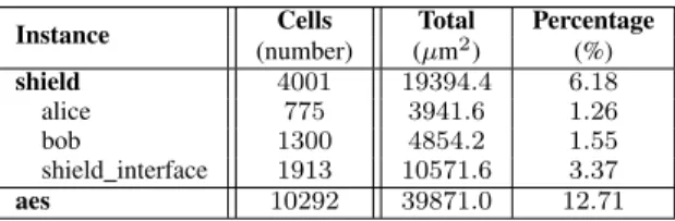
(number) (µm2) (%) shield 4001 19394.4 6.18 alice 775 3941.6 1.26 bob 1300 4854.2 1.55 shield interface 1913 10571.6 3.37 aes 10292 39871.0 12.71 C. Power
Table III gives an overview of the circuit power consumption reported by SOC-Encounter. This estimation is done by setting the frequency to 100 MHz and the core global activity to
1/2. The shield consumption is7.01 mW. It is composed of 2
parts: internal (gates) and switching (interconnection) power. By observing Table III, we notice that the switching power of Alice is the most important (4.04 mW) in the shield because of the capacitive mesh lines connected to Alice buffers. This formula shows the power computations of ICs:
PTotal = PInternal+PSwitching≈ pt· (EInternal+ESwitching)· Fclk .
The parameter ptis the probability of transition, which is close
to its maximal value (namely 1/2) for the ciphertext we use
as data in our shield. EInternalis the internal energy dissipated
by the IP: it depends on the number of standard cells used. ESwitching is the energy dissipated of the IPs connections which
is fixed when the core is placed and routed. For a circuit of x µm× y µm, the consumption of the shield can be estimated as PTotal≈ pt· (560y · (EInternal+560x · ESwitching))× Fclk .
As the dominant term is ESwitching from Alice (c.f. Tab. III),
the power consumption of the shield, quite naturally, grows proportionally to the circuit’s area x· y. The M7 lines have a capacitance of 150 fF and a resistance of 45 Ω. With a regular buffer (x2 drive), the propagation time is estimated by ELDO simulations to5 ns. A larger buffer (x18 drive, cell HS65_LS_BFX18) reduces the propagation time to0.3 ns.
In the PTotal formula, we see that the dissipated power is
proportional to the operating frequency Fclk, that we can
re-duced through the API instruction “Set freq” (recall Sec. II-E). This instruction thus allows to define a power management strategy at software level. It helps reduce significantly the shield consumption (a ratio of100 for a frequency of 1 MHz). In our prototype ASIC, we wished to study the coupling of
TABLE III
POWER CONSUMPTION OFIPS(IN MW),OPERATED AT100 MHZ
Instance Internal Power Switching Power Total
shield 1.54 5.47 7.01
alice 0.41 4.04 4.45
bob 0.30 0.80 1.10
shield interface 0.83 0.61 1.44
aes 2.16 3.87 6.03
the shield mesh activity on the underlying IPs (PUF, digital sensor, etc.). Therefore, we used fast buffers. However, in a commercial product, the shield would be operated at much lower frequencies. So, all shield standard cells can be replaced by low-power standard cells hence reduce EInternal. Another
possibility is to disable the shield all the time and activate it only during critical computations (for example cryptographic computations) via the API “Enable/Disable” instructions.
For this prototype ASIC, we did not make specific efforts to optimize the shield structure and synthesis. The shield clock tree was synthesized with the same constraints as the protected circuit (namely,100 MHz). With relaxed constraints, the clock tree would use less buffers. Besides, the comparator on Bob’s side is either on128 or on 5× 128 bits, but it can clearly be made smaller by trading silicon area for more time. So with these approaches and optimizations, the shield area and power consumption can be further reduced.
IV. PROTECTION AGAINSTBACKSIDEATTACKS
Despite reported hacks [20], conventional digital shielding provides a good level of protection against probing and FIB attacks but is actually inefficient regarding backside attacks. Backside attacks have been known for a long time and recent exploits [12] demonstrated the possibility of probing a device on the backside of the circuit (i.e., from the silicon substrate end) without altering it.
Backside access requires a special chip preparation. Once the circuit is thinned, the attacker can eavesdrop signal(s) and even modify the circuitry using advanced FIB techniques. Some recent works have shown that circuit edit is even possible on thick silicon devices [19], thus avoiding the ad-vanced thinning process normally needed in backside attacks. Figure 10 is presenting a piece of circuitry where an attacker has gained physical access to metal lines using backside FIB attack. After identifying the targeted line, the attacker digs a funnel using FIB to probe the inverter’s input. The attacker has successfully bypassed the top layer active shield and has gained physical access to a fully working circuit where he can read data and inject faults.
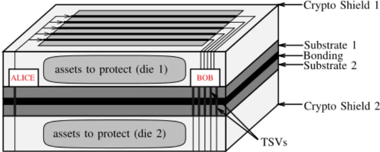
To address backside attacks, we can improve our crypto-graphically secure shield towards 3D integration [9]. Conven-tional active shields are inefficient regarding backside attacks, but by letting our meshes spread over several dies, we can protect a whole chip stack against all kinds of probing attacks. There are several trends in 3D technologies and depending on the one we are using, we can create different ways of
Top Layer Shield
N+
N+P+N+ P+ P+
Probed Line
Fig. 10. Side view of a thinned substrate probed on backside
Crypto Shield 2 Crypto Shield 1 Substrate 1 Substrate 2 Bonding BOB ALICE TSVs assets to protect (die 1)
assets to protect (die 2)
Fig. 11. Cryptographic shield spreading on two dies bonded back to back
shielding the chip stack. Figure 11 presents a back to back embodiment of two dies: the lowest die is oriented face-down while the top die is face-up. Logic signals are carried through TSVs across dies enabling the same logic to run both shields. In this configuration our cryptographic shield is forming a cage around the circuitry, preventing probing attacks from both side of the chip stack.
V. CONCLUSIONS ANDPERSPECTIVES
In this article, we have presented a new cryptographically-secure active shield architecture. This shield, based on a SI-MON lightweight block cipher, ensures the hardware security against probing and FIB attacks. We also demonstrated that the implementation of such shield is easy, through the tape-out of a 1 mm2 (core size: 560 µm× 560 µm) ASIC circuit. The extra cost in term of surface is less than 10 % and the extra cost in term of power consumption could be tuned by adjusting the mesh frequency. So, for some applications the implementation cost is acceptable. The larger the circuit, the smaller the overheads.
As a perspective, we intend to check the impact of this shield on side-channel attacks, such as electromagnetic (EM) leakage [11] and EM injection [22]. We expect EM leakage to be enhanced, since the sensitive information that is radiated by the IPs behind the shield (e.g., the AES) may be amplified by the mesh. On the contrary, we expect EM injections to be harder, since the EM pulses might be caught by the shield, thereby affecting less the power network.
ACKNOWLEDGEMENTS
The authors are grateful to Shivam Bhasin for the imple-mentation of the SIMON cipher, for communicating the attack methodology of SIMON using side-channel analysis, and for its low-cost protection method by a masking countermeasure.
REFERENCES
[1] Ray Beaulieu, Douglas Shors, Jason Smith, Stefan Treatman-Clark, Bryan Weeks, and Louis Wingers. The SIMON and SPECK Families
of Lightweight Block Ciphers. Cryptology ePrint Archive, Report
2013/404, 2013. http://eprint.iacr.org/2013/404.
[2] Andrea Beit-Grogger and Josef Riegebauer. Integrated circuit having an active shield, November 8 2005. United States Patent number 6,962,294. [3] Shivam Bhasin, Tarik Graba, Zakaria Najm, and Jean-Luc Danger. A Look into SIMON from a Side-Channel Perspective. In HOST, IEEE Computer Society, May 2014. Arlington, USA.
[4] S´ebastien Briais, St´ephane Caron, Jean-Michel Cioranesco, Jean-Luc Danger, Sylvain Guilley, Jacques-Henri Jourdan, Arthur Milchior, David
Naccache, and Thibault Porteboeuf. 3D Hardware Canaries. In
Emmanuel Prouff and Patrick Schaumont, editors, CHES, volume 7428 of LNCS, pages 1–22. Springer, 2012.
[5] S´ebastien Briais, Jean-Michel Cioranesco, Jean-Luc Danger, Sylvain
Guilley, David Naccache, and Thibault Porteboeuf. Random active
shield. In Guido Bertoni and Benedikt Gierlichs, editors, FDTC, pages 103–113. IEEE, 2012.
[6] Cat whisker tips. http://www.signatone.com/products/tips holders/. [7] Cat whisker tips. http://opspe.com/PS/cat whisker tips.html.
[8] Pawel Chodowiec and Kris Gaj. Very Compact FPGA Implementation of the AES Algorithm. In Colin D. Walter, C¸ etin Kaya Koc¸, and Christof Paar, editors, CHES, volume 2779 of Lecture Notes in Computer Science, pages 319–333. Springer, 2003.
[9] Jean-Michel Cioranesco and David Naccache. Protection of an integrated circuit against invasive attacks, August 7 2013. Patent EP 2624296 A1. [10] Thomas Eisenbarth, Zheng Gong, Tim G¨uneysu, Stefan Heyse, Sebas-tiaan Indesteege, St´ephanie Kerckhof, Franc¸ois Koeune, Tomislav Nad, Thomas Plos, Francesco Regazzoni, Franc¸ois-Xavier Standaert, and Lo¨ıc van Oldeneel tot Oldenzeel. Compact Implementation and Performance Evaluation of Block Ciphers in ATtiny Devices. In Aikaterini Mitrokotsa and Serge Vaudenay, editors, AFRICACRYPT, volume 7374 of Lecture Notes in Computer Science, pages 172–187. Springer, 2012.
[11] Karine Gandolfi, Christophe Mourtel, and Francis Olivier. Electromag-netic Analysis: Concrete Results. In CHES, volume 2162 of LNCS, pages 251–261. Springer, May 14-16 2001. Paris, France.
[12] Clemens Helfmeier, Dmitry Nedospasov, Christopher Tarnovsky, Jan Starbug Krissler, Christian Boit, and Jean-Pierre Seifert. Breaking and entering through the silicon. In Ahmad-Reza Sadeghi, Virgil D. Gligor, and Moti Yung, editors, ACM Conference on Computer and Communications Security, pages 733–744. ACM, 2013.
[13] INVIA. Active Shield IP (digital IP and analog IP that detects invasive attacks). http://invia.fr/detectors/active-shield.aspx.
[14] Marcus Janke and Korbinian Engl. Integrated circuit and method of protecting a circuit part to be protected of an integrated circuit, January 7 2010. US Patent App. 12/166,906.
[15] Peter Laackmann and Hans Taddiken. Apparatus for protecting an
integrated circuit formed in a substrate and method for protecting the circuit against reverse engineering, February 19 2003. United States Patent number 6,798,234.
[16] James Liddle. Robust hardware security devices made possible by
laser direct structuring, December 2012. ECN (Electronic Component News) Magazine; Online: http://www.ecnmag.com/articles/2012/04/ robust-hardware-security-devices-made-possible-laser-direct-structuring. [17] Alfred J. Menezes, Paul C. van Oorschot, and Scott A. Vanstone.
Handbook of Applied Cryptography. CRC Press, October 1996. [18] Andrew H. Olney. Characterization of Integrated Circuits by Qualitative
Voltage Contrast Imaging in the Scanning Electron Microscope. Boston University, 1988.
[19] Chad Rue, Steven B. Herschbein, and Carmelo F. Scrudato. Backside Circuit Edit on Full-thickness Silicon Devices. In Proc. 34th Int. Symp. Test and Failure Analysis (ISTFA), pages 141–150. ASM International, November 2008.
[20] Christopher Tarnovsky. Infineon / ST Mesh Comparison, February 14th 2010. http://blog.ioactive.com/2010/02/infineon-st-mesh-comparison. html.
[21] Randy Torrance and Dick James. The State-of-the-Art in IC Reverse Engineering. In CHES, volume 5747 of LNCS, pages 363–381. Springer, September 6-9 2009. Lausanne, Switzerland.
[22] Fabian Vargas, D. L. Cavalcante, E. Gatti, D´arcio Prestes, and D. Lupi.
IOLTS, pages 207–208. IEEE Computer Society, July 6-8 2005. Saint Rapha¨el, France.
[23] Richard Young and Peter Carleson. [Dual-beam FIB/SEM] A Tool for Advanced Failure Analysis, September 2004. EE online magazine, http: //www.evaluationengineering.com/.