Selective epitaxial growth of III-V semiconductor heterostructures on Si substrates for logic applications
N. D. Nguyena,b, G. Wanga, G. Brammertza, M. Leysa, N. Waldrona, G. Winderickxa, K. Lismonta, J. Dekostera, R. Looa, M. Meurisa, S. Degrootea, F. Buttitac, B. O'Neilc,
O. Féronc, J. Lindnerc, F. Schultec, B. Schinellerc, M. Heukenc and M. Caymaxa
a
imec, Kapeldreef 75, B-3001 Leuven, BELGIUM
b
Institute of Physics, University of Liège, B-4000 Liège, BELGIUM
c AIXTRON AG, Kaiserstrasse 98, D-52124 Herzogenrath, GERMANY
We have deposited III-V alloys on 200 mm Si miscut wafers with an oxide pattern. The selective epitaxial growth (SEG) of GaAs in large windows defined by SiO2 lines on a thick strained-relaxed Ge
buffer layer served as a test vehicle which allowed us to demonstrate the integration of a III-V material deposition process step in a Si manufacturing line using an industrial reactor. High quality GaAs layers with high wafer-scale thickness uniformity were achieved. In a subsequent step, SEG of InP was successfully performed on wafers with a 300 nm shallow trench isolation pattern. The seed layer morphology depended on the treatment of the Ge surface and on the growth temperature. The orientation of the trench with respect to the substrate miscut direction had an impact on the quality of the InP filling. Despite of the challenges, such an approach for the integration of III-V materials on Si substrates allowed us to obtain extended-defect-free epitaxial regions suitable for the fabrication of high-performance devices.
Introduction
Sub-22 nm high-performance digital circuits based on metal-oxide semiconductor (MOS) devices call for the introduction of non-Si channel materials such as Ge for pMOS and III-V compounds for nMOS. InP and other high-electron mobility materials such as InxGa1-xAs have been advantageously used for decades through band gap engineering in
various applications ranging from high-power, high-frequency electronics to optoelectronics, [1-2]. Although tremendous progress has been accomplished in the compound semiconductor industry, most devices in production nowadays are discrete due to the unavailability of cheap substrates. Therefore, the integration of arsenide and phosphide materials into a mainstream Si process line is considered as one of the most promising and cost-effective manufacturing options which would allow the industry to fully leverage the wafer size and state-of-the-art complementary MOS (CMOS) Si processing equipments [3].
The successful integration of these semiconductors on Si substrates relies on the deposition of thin layers without extended defects. A technical solution which gives encouraging results to the achievement of this task is provided by the selective epitaxial growth (SEG) of the required materials in shallow trench isolation (STI) structures. This
approach, based on the extended defect necking effect [4-6], alleviates the large lattice mismatch between the III-V semiconductors and the Si substrate and leads to defect-free regions in the filled STI structure, on which devices can be fabricated. However, additionally to the challenge of hetero-epitaxial growth of a polar semiconductor on a non-polar surface, other issues, related to the generation of undesired stacking faults or twin defects, have to be solved. Furthermore, in the perspective of application in a standard low-cost very-large-scale integration (VLSI) scheme, these high-mobility materials have to be fabricated on large-area Si substrates in order to meet the requirements of the CMOS industry.
In this work, we report results on the epitaxial growth of III-V alloys on 200 mm Si wafers by means of metal-organic chemical vapor deposition (MOCVD). The paper is organized as follows. The experimental procedure is first described. We then study the selective growth of GaAs on strain-relaxed Ge-on-Si (GOS) templates. This serves as a test vehicle and allowed us to identify and solve the hurdles associated to the implementation of a III-V deposition step in an industrial CMOS process flow. The generated know-how is then applied to tackle the challenge of selective growth of InP on wafers with STI pattern. Final remarks are given in the conclusion part.
Experimental details
Our processes were developed using a specially-designed Crius Close-Coupled Showerhead MOCVD system from AIXTRON AG [7]. The formation of anti-phase domain (APD) boundaries, which lead to strong detrimental effects on the electrical properties of the epilayer, was avoided by the use of oriented Si (100) wafers (6° off-orientation toward <111>).
For the growth of GaAs, a 1 µm thick Ge buffer was first deposited on the Si wafer in a separate CVD chamber. The details of the fabrication of this template, which also includes a chemical and mechanical planarization (CMP) step, are described elsewhere [8]. This epitaxial, strain-relaxed, Ge layer serves as an intermediate buffer between the substrate and the III-V material. The lattice mismatch between the substrate and the layer is nearly totally accommodated and, thus, no additional threading dislocation is introduced in the deposited III-V film. In contrast to Si surfaces, the Ge buffer also allows us to work with a reduced thermal budget for the in-situ pre-epi surface clean. An SiO2 grid pattern was processed on top of the Ge layer, defining 200 µm × 1200 µm
windows with an exposed active area ratio of about 97% of the total wafer surface. After a standard NH4OH/H2O2 clean, the wafers were loaded into the reactor and received an
in-situ bake at reduced pressure under tertiarybutylarsine (TBAs), H2 being used as
carrier gas. Trimethylgallium (TMGa) was used as the group-III precursor and TBAs as source for the group-V element.
Selective growth of InP was performed in 300 nm deep trenches made with SiO2 STI
patterning. The width of the trenches ranges from 0.1 to 100 µm. About 40% of the total Si wafer surface is exposed to deposition. Process details of the Ge buffer deposition in the trenches are given in Ref. [6]. After being loaded into the MOCVD chamber, the wafers received an in-situ bake similar to the one described here above and InP was grown using trimethylindium (TMIn) and tertiarybutylphosphine (TBP) as precursors. A
seed layer of about 40 nm was first grown at 420°C, followed by the growth of the main layer at 610°C.
Results and discussion
Selective growth of GaAs on 200 mm strain-relaxed Ge-on-Si templates
The use of a relaxed Ge buffer layer deposited on an off-axis cut Si wafer is an elegant way to simultaneously suppress the formation of APDs and accommodate the initial lattice mismatch of 4% between Si and GaAs. Upon loading the GOS template into the MOCVD tool, the standard growth procedure for GaAs started with a bake at 670°C which favored the merging of single atomic steps on the 6° toward (111) miscut (100) surface into energetically more stable double steps. A larger TBAs flow at the end of the bake then led to a complete and self-limiting coverage of the Ge surface with As atoms by the achievement of a sufficient As partial pressure which prevented desorption [9]. A nucleation layer was first grown under a total pressure of 600 mbar and with a V/III ratio of 110 and a growth rate of about 0.2 nm/s. Process parameters were subsequently ramped without growth interruption to reach a pressure of 50 mbar and a V/III ratio of about 17 with a growth rate of 1.2 nm/s.
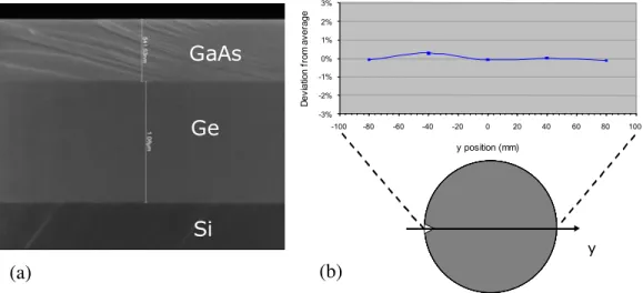
These conditions produced smooth, mirror-like, grown GaAs layers. A scanning electron microscope (SEM) image of the cross section of the epitaxial structure is shown in Fig. 1a, depicting the GaAs/Ge layer stack on the Si substrate. A diameter profile of the GaAs thickness, obtained from direct SEM inspection at 5 points (Fig. 1b), revealed an excellent uniformity of 0.2% (1σ) over the wafer with an average value of 540 nm.
GaAs Ge Si GaAs Ge Si
GaAs thickness prof ile
-3% -2% -1% 0% 1% 2% 3% -100 -80 -60 -40 -20 0 20 40 60 80 100 y position (mm) De vi at io n fr om a ve ra ge
GaAs thickness prof ile
-3% -2% -1% 0% 1% 2% 3% -100 -80 -60 -40 -20 0 20 40 60 80 100 y position (mm) De vi at io n fr om a ve ra ge y
Fig. 1. (a) SEM image of the cross section of the GaAs/Ge/Si layer stack and (b) GaAs thickness profile.
Photoluminescence (PL) spectroscopy, which is a highly sensitive characterization technique for GaAs, confirmed the excellent crystal quality of the deposited layers. In Fig. 2, the PL intensity as function of the photon energy from an np junction is comparable to that of a reference sample [10]. The epitaxial structure was grown using a
similar growth process; in-situ doping was performed with SiH4 and CCl3Br to introduce
Si and C as n-type and p-type dopants into GaAs with nominal concentrations of 3E17 cm-3 and 1E18 cm-3, respectively.
0 0.2 0.4 0.6 0.8 1 1.2 1.4 1.6 1.44 1.46 1.48 1.5 1.52 1.54 Energy (eV) PL I n te n s it y ( a . u .)
1000 nm 2e17 Si-doped GaAs on Ge (Thomas Swan 2006)) 1000 nm 3e17 Si-doped GaAs on Ge (Crius 2009)
Reference sample [10] This work
Fig. 2. PL spectra of a np GaAs junction grown in this work and of a similar reference structure [10].
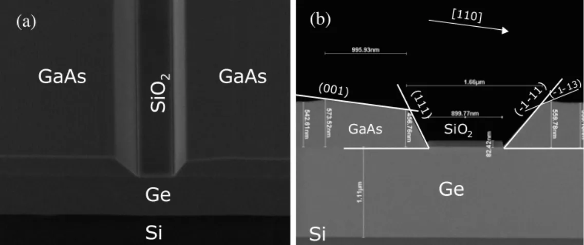
The optimized growth conditions prevented nucleation of GaAs on SiO2 and thus
allowed us to achieve very high selectivity of the process on patterned wafers, as shown in Fig. 3. The facets observed along the {111} and {113} directions are well-known effects of the selective growth of GaAs [11, 12]. The surface roughness, as measured by atomic force microscopy, was in the range 1.15 – 1.25 nm, root-mean-square (RMS) value. SiO 2 GaAs GaAs Ge Si (001) (1 11) (- 1-11) [110] (-1-13) GaAs SiO2 Ge Si
Fig. 3. (a) Tilted cross-section SEM view of GaAs selectively grown on a SiO2-patterned
GOS template and (b) normal cross-section SEM view. The oxide line is 1 µm wide. Although the roughness of the GaAs layer is higher than that of the starting GOS surface (typically 0.55 nm RMS), capacitor structures were successfully fabricated using an integration process flow very similar to standard high volume Si manufacturing lines. The capacitance-voltage characteristics were similar to the ones obtained on a bulk GaAs
substrate, and showed extremely tight within-wafer and wafer-to-wafer distributions as is standard to Si manufacturing. The detailed results are presented elsewhere.
Selective growth of InP in narrow trenches
The purpose of the in-situ bake of the Ge buffer layer (about 40 nm at the bottom of the trench) under TBAs is to favor a good nucleation of the InP seed layer. A study of the annealing of Ge surfaces in As ambient showed that a high AsH3 partial pressure
enables the formation of Ge double steps whereas single steps were consequent to a low AsH3 partial pressure [13]. We assume that a similar mechanism applies for TBAs,
resulting in the adsorption of a monolayer of As which can change the initially non-polar Ge surface into a polar surface and thus facilitates the subsequent nucleation of InP. Moreover, stacking fault (SF) density can be reduced by an As-terminated Ge surface because of the lower density of InP islands at the early stage of the growth, which is due to the retardation of In adatom diffusion by the surfactant effect of the As coverage. One should note that due to its surface roughness of 0.50 nm RMS, the atomic steps of the offcut Si substrate are not copied to the surface of the Ge buffer. However, double steps are formed after the pre-epi bake, emphasizing the importance of an adequate choice of the bake conditions [14].
With a strain-relaxed Ge layer, the lattice mismatch between the InP layer and the substrate reduces from 8% to 3.7%. Figure 4 shows the impact of the growth temperature on the surface morphology of InP seed layers grown at 400°C and 420°C. The total pressure, the TBP flow and the V/III ratio were constant with values of 500 mbar, 600 sccm and 370, respectively. Growth at 400°C (average surface temperature) occurred in the regime of catalytic decomposition of TBP. At that temperature, the cracking of the TBP precursor is not complete and the thermal budget does not allow to overcome the activation energy barrier associated to the reaction of P with In, whose precursor has a lower cracking temperature. As a result, InP nanowires were obtained and no complete layer could be formed on the Ge surface (Fig. 4a). At the temperature of 420°C, both TBP and TMIn are decomposed, leading to the deposition of a smooth seed layer (Fig. 4b). Figure 4c shows the morphology of the InP seed inside a typical trench under optimal nucleation conditions, highlighting the full coverage of the trench by the nucleation layer.
1 µm 1 µm 500 nm
Ge + InP ~ 90 nm
Fig. 4. SEM images of the morphology of the seed layer in a large area pad at (a) 400°C and (b) 420°C, as well as (c) inside a typical trench.
The morphology of the InP nucleation layer on the Ge buffer thus depends on the pre-epi bake ambient conditions and expresses a high sensitivity on the deposition temperature. The impact of the InP seed on the overall quality of the layer grown in the trench is important as a smooth seed layer could lead to the reduction of extended defects and resulted in vertical crystal growth above the STI surface whereas a rougher seed induced distorted overgrowth.
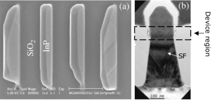
Si O2 InP De vi ce re g io n SF
Fig. 5. (a) Top view SEM image of 150 nm wide and 3 µm long InP-filled STI structures. (b) TEM cross-section image of a trench with InP overgrowth.
Excellent selectivity of the InP growth with respect to SiO2 could be demonstrated, as
shown in Fig. 5a. We also studied the formation of crystal facets and of stacking faults (SF), which are commonly observed in strain-relaxed III-V compound semiconductors epitaxially grown on Si (001) or Ge (001) because of their lower energies in such alloys compared to those in Si or Ge. Facet and SF formation depends on the trench orientation [14]. Symmetric {111} facets were observed in trenches along [110] but not in trenches oriented in the [-110] direction. SFs in trenches along [110], which originated from the dissociation of threading dislocations, could be trapped on the bottom when an aspect ratio greater than 2 was used. In such a case, extended-defect-free InP material could be obtained in the top region, as shown in Fig. 5b.
After a planarization step, the InP layer can serve as a virtual substrate for the subsequent growth of the lattice-matched In0.53Ga0.47As ternary compound as channel
material, the discussion of which is beyond the scope of this paper. In Fig. 6, we show an SEM image of typical planarized InP-filled trenches. The wider band gap of InP also provides a potential barrier which can prevent electrical leakage through the substrate.
Fig. 6. Top view SEM image of InP-filled trenches after planarization.
Conclusions
We have studied the selective growth of III-V compound semiconductors on 200 mm patterned Si wafers using an specially-designed MOCVD reactor. This illustrated the integration of a III-V epitaxial deposition step into a Si CMOS manufacturing line. An InP SEG process on STI structures was developed to enable extended-defect-free regions on which devices could be fabricated. Our results highlighted the significant challenges faced by epi process technologists to achieve a successful combination of Ge and III-V materials on one Si substrate, which is key to high performance CMOS devices.
Acknowledgments
Financial support from the European Union FP7 ‘DUALLOGIC’ project, contract number 213238, is gratefully acknowledged.
References
1. F. Capasso, Science 235, 172 (1987).
2. M. Behet, R. Hövel, A. Kohl, A. Mesquida Küsters, B. Opitz and K. Heime, Microelectron. J. 27, 297 (1996).
3. E. Fitzgerald, M. Bulsara, Y. Bai, C. Cheng, W. K. Liu, D. Lubyshev, J. M. Fastenau, Y. Wu, M. Urtega, W. Ha, J. Bergman, B. Brar, C. Drazek, N. Daval, F. Leterte, W. E. Hoke, J. R. LaRoche, K. J. Herrick and T. E. Kazior, ECS Trans.
16(10), 1015 (2008)
4. T. A. Langdo, C. W. Leitz, M. T. Currie, E. A. Fitzgerald, A. Lochtefeld and D. A. Antoniadis, Appl. Phys. Lett. 76, 3700 (2000).
5. J. Z. Li, J. Bai, J. M. Hydrick, J. G. Fiorenza, C. Major, M. Carroll, Z. Shellengarger and A. Lochtefeld, ECS Trans. 18(1), 887 (2009).
6. G. Wang, R. Loo, S. Takeuchi, L. Souriau, J. C. Lin, A. Moussa, H. Bender, B. De Jaeger, P. Ong, W. Lee, M. Meuris, M. Caymax, W. Vandervorst, B. Blanpain and M. M. Heyns, Thin Solid Films 518, 2538 (2010).
7. B. Schineller, N. D. Nguyen and M. Heuken, ECS Trans. 28(5), 233 (2010). 8. G. Wang, R. Loo, E. Simoen, L. Souriau, M. Caymax, M. M. Heyns and B.
Blanpain, Appl. Phys. Lett. 94, 102115 (2009).
9. G. Brammertz, Y. Mols, S. Degroote, M. Leys, J. Van Steenbergen, G. Borghs and M. Caymax, J. Cryst. Growth 297, 204 (2006).
10. G. Brammertz, Y. Mols, S. Degroote, V. Motsnyi, M. Leys, G. Borghs and M. Caymax, J. Appl. Phys. 99, 93514 (2006).
11. Y. Kohama, Y. Kadota and Y. Ohmachi, Jpn. J. Appl. Phys. 29, L229 (1990). 12. T. Yamada and Y. Horikoshi, Jpn. J. Appl. Phys. 33, L1027 (1994).
13. W. E. McMahon and J. M. Olson, Phys. Rev. B 60, 2480 (1999).
14. G. Wang, N. D. Nguyen, M. R. Leys, R. Loo, G. Brammertz, O. Richard, H. Bender, J. Dekoster, M. Meuris, M. M. Heyns and M. Caymax, ECS Trans. 27(1), 959 (2010).