Electrical Characterization of InGaN/GaN Multiple-Quantum-Well
Structures by Thermal Admittance Spectroscopy
N. D. NGUYEN (a), M. SCHMEITS (a), M. GERMAIN (a), B. SCHINELLER (b), and M. HEUKEN (b, c)
(a) Institut de Physique, Université de Liège B5, 4000 Liège, Belgium (b) AIXTRON AG, Kackertstr. 15-17, 52072 Aachen, Germany
(c) Institut für Halbleitertechnik, RWTH Aachen, Templergraben 55, 52056 Aachen, Germany
PACS: 73.40.-c; 73.61.Ey; 73.63.Hs; 84.37.+q
Abstract
Experimental results of electrical characterization of InGaN/GaN multiple-quantum-well electroluminescence test structures obtained by thermal admittance spectroscopy are presented. The studied GaN:Mg/5 × (InGaN/ GaN)/GaN:Si structures were grown on c-plane sapphire substrate by metal-organic vapor phase epitaxy. Admittance measurements were conducted from room temperature down to 125 K for a wide frequency range and for different applied bias voltages. Analysis of the capacitance versus frequency curves shows the presence of several cutoff frequencies which originate from the response of equivalent RC series circuits and give peaks in the conductance divided by angular frequency. The dependence of the position and the amplitude of these peaks on temperature is discussed.
1. Introduction
Nitride semiconductors have attracted much attention during the past decade as they are used for the fabrication of short-wavelength light-emitting diodes (LEDs) [1] and laser diodes [2]. The InGaN alloy has become the major building block of these devices due to the tunability of its energy gap which covers the visible to near ultraviolet light spectra. It is used in quantum structures such as InGaN/GaN multiple-quantum-well (MQW) emitters. Admittance measurements of these structures are of importance as they contribute to the understanding of current transport in these devices. Such studies have been performed previously on QW systems, but mostly on GaAs or Si-based structures [3, 4].
2. Experiment
The studied electroluminescence test (ELT) structure was grown by metalorganic chemical vapor deposition (MOCVD) on sapphire substrate. An approximately 25 nm thick GaN nucleation layer was first deposited at low temperature, followed by a 0.9 µm thick unintentionally doped GaN layer and a 1.2 µm thick Si-doped (3 × 10¹⁸
cm-3) GaN layer. The active region consists of a fivefold InGaN/GaN:Si (2 nm/7 nm) multiquan-tum well, on top
of which a 100 nm thick GaN:Mg layer was deposited. The admittance of the structure was measured with a Hewlett-Packard 4192A LF admittance analyzer for frequencies in the range of 100 Hz to 3 MHz and for bias voltages from -3 to +3 V. The temperature of the sample was varied from 125 K up to room temperature (RT, 293 K).
3. Results and Discussion
In Fig. 1 the thermal admittance spectroscopy (TAS) data obtained for the ELT structure are presented. The frequency responses of the capacitance C and the conductance G divided by the angular frequency ω = 2πf, where ƒ is the measurement frequency, are shown for temperatures T ranging from 275 to 125 K and zero applied voltage. At the highest temperatures, the capacitance exhibits a plateau regime for frequencies up to 30 kHz followed by a transition region where the capacitance decreases down to a high frequency value which is dependent on the temperature. For T < 170 K, the plateau regime is reduced below 1 kHz and could not be observed due to the limitation of the resolution of the measurements at low frequency. As the temperature is lowered, the transition region apparently widens and is shifted towards lower frequencies, while a variation of the slope can be observed between 100 kHz and 1 MHz for the lowest temperatures. The large peak centered at 250 kHz in the G/ω curve for T = 275 K corresponds to the mean cutoff frequency in the capacitance curve. When the temperature is decreased, the position of this peak is shifted towards the low frequencies while its amplitude is reduced. For temperatures below 230 K, we can observe a shoulder which arises from the high frequency region and resolves itself as a second structure for T < 125 K.
Published in: Physica Status Solidi C. Current Topics in Solid State Physics (2002), n° 1, pp. 288-292 Authors : N. D. Nguyen, M. Schmeits, M. Germain, B. Schineller, and M. Heuken
The presence of a peak in the G/ω curves suggests that the frequency response of the MQW structure to an ac voltage excitation is similar to that of an electrical RC series circuit, with a peak frequency fc = 1/(2πRC)
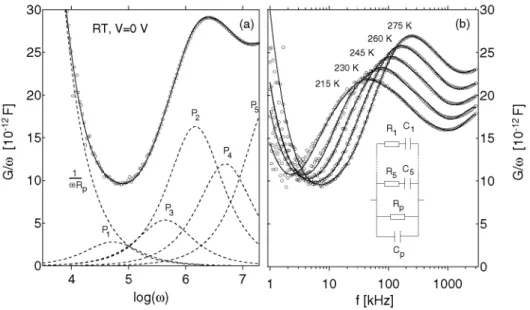
corresponding to a cutoff in the capacitance curve. However, in this case, the width of this peak cannot be related to a single RC circuit. Indeed the full width at half magnitude (FWHM) of the G/ω peak corresponding to the ac response of a single RC series circuit has a value of ∆(log (2πf)) = log [(2 + √3)/(2 - √3)] ≈ 1.14 which is independent on the values of the resistance R and the capacitance C. The estimated FWHM of the observed peak is larger than 1.14, it therefore cannot correspond to a single equivalent RC series circuit. An optimized fit procedure has been used to determine the composition of the equivalent circuit which would reproduce the various experimental admittance curves. The resistive and capacitive elements contained in the fit model are temperature and voltage-dependent. In this work, we focus on the temperature dependence of the various Rj and Cj components. In Fig. 2a we show the fitting of G/ω at room temperature by the equivalent electrical circuit [5] represented as inset. The RC series circuits simulate the ac behavior of the quantum wells while the resistance Rp
could represent the effect of a recombination current path or a leakage current, and Cp the depletion capacitance.
The values of Rj and Cj are generally functions of the temperature, yielding a dependence of each cutoff
frequency fc,j = 1/(2πRjCj) on the temperature. Results of the fitting are shown in Fig. 2b for temperatures
between 215 and 275 K. For T < 245 K, the RC component with the lowest cutoff frequency yields no contribution, reducing the model to four RC series circuits in parallel with Rp and Cp.
The equivalent electrical circuit model used for the fitting of G/ω also reproduces the measured impedance of the ELT structure. In Fig. 3, the obtained curves of the real and imaginary parts of the impedance Z are shown with the capacitance C and G/ω curves. The cutoff frequency fc,s = 1/(2πRsCp), where Rs is the series resistance, would
appear at higher frequencies, leading to an additional peak in G/ω curves. But its position would fall outside the measurement range. It was therefore not included in this analysis.
Activation energies related to defect levels can be obtained by a classical interpretation of TAS data [6, 7]. Although one should be careful when using such a method [8], this type of analysis has been applied to QW structures, either to assess the presence of defects [9] or to determine QW parameters [10]. The Arrhenius plot of the cutoff frequencies corresponding to the five RC series circuits, shown in Fig. 4, gives values of the activation energies ranging from 32 to 248 meV with an accuracy of about 10%. The observed cutoff frequencies fc,j could
therefore be related to a thermionic activation mechanism of the QWs [4]. The obtained values of the activation energies cover a large range, which may be an indication of the existence of discrepancies in the composition of the InGaN alloy or in geometrical parameters of the QWs. Further investigations, based on the solution of the basic semiconductor equations [8] for the ELT structure, are being performed in order to clarify the microscopic origin of the activation energies.
Acknowledgements This work has been financially supported by the INTAS grant No. N97-0995. We gratefully
acknowledge the cooperation of E. Smalbrugge, Eindhoven University of Technology.
Fig. 1. Experimental curves of a) capacitance C and b) conductance G divided by the angular frequency ω, for
zero applied voltage. The temperature was varied from 275 down to 125 K by steps of -15 K Published in: Physica Status Solidi C. Current Topics in Solid State Physics (2002), n° 1, pp. 288-292
Authors : N. D. Nguyen, M. Schmeits, M. Germain, B. Schineller, and M. Heuken Status Postprint (Author’s version)
Fig. 2. a) Fit of G/ω curve at room temperature (RT) and zero bias (full line). Dashed lines show the
contributions of the different RC series circuits (P1 to P5) and of Rp; b) complete results of the fitting procedure
for G/ω at temperatures between 275 and 215 K. The inset in b) shows a schematic representation of the equivalent electrical circuit used in the fit procedure for T > 245 K
Fig. 3. Experimental (circles and squares) and fitted (full line) curves of a) Re(Z) and -Im(Z), b) C and G/ω at
room temperature (RT) and zero applied voltage, where Z is the impedance
Fig. 4. Arrhenius plot of the cutoff frequencies fc,j = 1(2πRjCj) of the five RC series circuits
References
[1] S. NAKAMURA,T. MUKAI,and M. SENOH,J. Appl. Phys. 76, 8189 (1994).
[2] S. NAKAMURA,M. SENOH,S. NAGAHAMA,N. IWASA,T. YAMADA,T. MATSUSHITA,H. KIYOKU,and Y. SUGIMOTO,Appl. Phys. Lett. 68, 3269 (1996).
Published in: Physica Status Solidi C. Current Topics in Solid State Physics (2002), n° 1, pp. 288-292 Authors : N. D. Nguyen, M. Schmeits, M. Germain, B. Schineller, and M. Heuken
[3] M. ERSHOV,B.YALDIZ,A. G. U. PERERA,S. G. MATSIK,H. C. LIU,M. BUCHANAN,Z. R. WASILEWSKI, and M. D. WILLIAMS,Infrared Phys. Technol. 42, 259 (2001).
[4] D. V. LANG,M. B. PANISH,F. CAPASSO,J. ALLAM,R. A. HAMM,A. M. SERGENT,and W. T. TSANG, Appl. Phys. Lett. 50, 736 (1987). [5] W. A. STRIFLER and C. W. BATES JR.,J. Appl. Phys. 71, 4358 (1992).
[6] J. W. HUANG,T. F. KUECH,H. LU,and I. BHAT,Appl. Phys. Lett. 68, 2392 (1996).
[7] D. J. KIM,D. Y. RYU,N. A. BOJARCZUK,J. KARASINSKI,S. GUHA,S. H. LEE,and J. H. LEE,J. Appl. Phys. 88, 2564 (2000). [8] N. D. NGUYEN,M. GERMAIN,M. SCHMEITS,B. SCHINELLER,and M. HEUKEN,J. Appl. Phys. 90, 985 (2001).
[9] M. OSINSKI,K. ZELLER,P. C. CHIU, B. S. PHILIPPS,and D. L. BARTON,Appl. Phys. Lett. 69, 898 (1996).
[10] A. Y. POLYAKOV, N. B. SMIRNOV, A. V. GOVORKOV, J. KIM, B. LUO, R. MEHANDRU, F. REN, K. P. LEE,S. J. PEARTON,A. V. OSINSKY,and P. E. NORRIS,J. Appl. Phys. 91, 5203 (2002).
Published in: Physica Status Solidi C. Current Topics in Solid State Physics (2002), n° 1, pp. 288-292 Authors : N. D. Nguyen, M. Schmeits, M. Germain, B. Schineller, and M. Heuken