UNIVERSITE MOHAMMED V FACULITE DES SCIENCES Rabat
N° d’ordre : 2729
THESE DE DOCRORAT
Présentée par
Sufyan Saleh Ahmed NAJI
Discipline: Physique informatique.
Spécialité : Matière condensée et modélisation des systèmes
A theoretical study on physical properties of 2D hexagonal
nanostructured materials
Soutenue le 23
Septembre 2014
Devant le jury :
Président :
Abdelilah BENYOUSSEF
PES, Faculté des Sciences, Rabat
Examinateurs :
Lahoucine BAHMAD
PES, Faculté des Sciences, Rabat
Mohamed BENAISSA
PH, Faculté des Sciences, Rabat
Youssef EL AMRAOUI
PES, Faculté des Sciences et Techniques, Errachidia
Abdallah EL KENZ
PES, Faculté des Sciences, Rabat
Hamid EZ-ZAHRAOU
PES, Faculté des Sciences, Rabat
El Kebir HLIL
PES, Institut NEEL, CNRS, Grenoble, France
Mohamed LOULIDI
PES, Faculté des Sciences, Rabat
Faculté des sciences, 4 Avenue Ibn Battouta B.P. 1014 RP, Rabat-Maroc Tel +212 (0) 37 77 18 34/35/38, Fax: +212 (0) 37 77 42 61, http:/www.fsr.ac.ma
Dedication
To
My father and mother
My wife Abeer
My children NOOR and Mohammed
To my brothers and sisters
To all my professors and teachers
To all my friends
Acknowledgement
This thesis has been carried out at the Laboratory of Magnetism and High Energy Physics (LMPHE), Faculty of Science, Mohammed V University – Rabat, under the supervision of prof. Abdelilah Benyoussef.
First and foremost, praises and thanks go to Allah, the Almighty, for his unlimited and uncountable blessings in my whole life and throughout my research work especially.
On this page, I would like to express my very great appreciation, deep gratitude and sincere thanks to my supervisor, the chairman of the jury prof. Abdelilah Benyoussef, for giving me this opportunity to learn from his valuable expertise and to have the fruitful discussions with him. He always had time to answer my questions and he patiently provided the vision, encouragement and advise necessary for me to proceed throughout my research period. It is my privilege to be his student.
Besides my supervisor, I would like also to offer my thanks to the thesis committee for reviewing my thesis and giving their insightful and useful comments.
I would like to thank Prof. Lahoucine Bahmad from Faculty of Science Rabat, for reviewing my PhD thesis.
I would like also to express my thanks to Prof. Abdallah EL Kenz from Faculty of Science Rabat , for reporting and reviewing this thesis.
I would like to thank Prof. Hamid EZ-Zahraouy from Faculty of Science Rabat, for reviewing this PhD thesis.
I would like also to offer my thanks to Prof. Mohamed Loulidi from Faculty of Science Rabat, for reviewing this thesis.
I would also like to extend my thanks to Prof. Mohamed Benaissa from Faculty of Science Rabat, for reviewing my thesis.
I would like also to express my thanks to Prof. El Kebir Hlil from University of Joseph Fourier, Grenoble, Institut Néel, France, for reporting and reviewing this PhD thesis.
II
I would like also to offer my thanks Prof. Youssef EL Amraoui from Faculty of Science and Technology, Errachidia, for reviewing this thesis.
I would like also to offer my special thanks to all the professors of our laboratory for their valuable suggestions and discussions.
I would also like to extend my thanks to the researchers Dr. H. Labrim, prof. A. Belhaj, Mr. M. Bhihi, Dr. B. Khalil for the interesting discussions and contributions. My thanks also go to my colleagues especially, Ms. F. El Hallani, Mr. D. Larhris, Mr. M. Lakhal, Miss M. El khatabi, Miss. H. Zaari, Mr. M. Abdellaoui, Mr. M. Boujnah, and Mr. N. Lakouari
I would like to thank the two following groups: prof. M. Richter and FPLO group and prof. P. Blaha, prof. K. Schwartz and WIEN2K group, for the support of FPLO and WIEN2K packages and for useful discussions.
Special thanks should be given to my wife Abeer, my daughter Noor and my son Mohammad, for their support, patience and encouragement throughout my study.
III
Abstract
In this thesis, we have theoretically investigated, using ab initio calculations, the electronic structure of graphene, silicene and germanene nanostructures.
We have shown first that, the inter-distances variation of the graphene bilayer affects the electronic properties that drastically depend on stacking arrangements. The interactions in such system lead to the opening of the band gap energy making this system extremely appealing for electronic devices and optoelectronics applications. A similar study has been also extended to silicene and germanene like bilayer systems which give close behaviors and results.
We have also engineered a double hexagonal structure model based on the adsorbed materials (Fe, Co, or Ni) atoms interacting with a graphene sheet. A close inspection shows that Fe-graphene and Co-graphene systems are ferromagnetic with strong spin polarizations, while Ni-system remains a non-magnetic metal. Monte Carlo calculations show that Co-graphene system has a high critical temperature making it a very useful in spintronic field. Besides that, we have proposed and examined a new hexagonal structure for C, Si and Ge atoms. It is found that, this new hexagonal structure modified the usual electronic properties, appearing in the single hexagonal geometries.
Keywords:Graphene, silicene and germanene nanostructures, ab initio calculations, Monte Carlo simulation, opening of the band gap energy, ferromagnetic with a strong spin polarization.
IV
Résumé
Dans cette thèse, nous avons étudié théoriquement, en utilisant des calculs ab initio, la structure électronique des nanostructures graphène, silicene et germanene.
Nous avons montré tout d'abord que, la variation de l’inter-distance de la bicouche de graphène affecte les propriétés électroniques qui dépendent fortement des configurations d'empilement. Les interactions, dans un tel système, conduisent à l'ouverture de l'énergie de la bande interdite qui rend ce système extrêmement attrayant pour des dispositifs électroniques et des applications optoélectroniques. Une étude similaire a été également étendue au silicene et germanene comme des systèmes bicouches qui donnent des comportements et des résultats proches.
Nous avons également conçu un modèle de la double structure hexagonale sur la base des éléments adsorbées (Fe, Co, ou Ni) interagissant avec une feuille de graphène. On constate que les systèmes Co-graphène et Fe-graphène sont ferromagnétiques avec une forte polarisation des spins, tandis que le système Ni-graphène reste non magnétique. Des calculs Monte Carlo montrent que le système Co-graphène a une haute température critique ; cette caractéristique est très utile dans le domaine de la spintronique.
En plus de cela, nous avons proposé et examiné une nouvelle structure hexagonale pour les atomes C, Si et Ge. Il se trouve que, cette nouvelle structure hexagonale a modifié les propriétés électroniques, figurant dans les géométries hexagonales simples.
Mots-clefs: Nanostructures, graphène, silicene et germanene, calculs ab initio, la simulation Monte Carlo, l'ouverture de l'énergie de la bande interdite, ferromagnétiques avec une forte polarisation des spins.
V
Résumé Détaillé
Cette thèse porte sur l’étude théorique, basée sur le calcul ab initio et la simulation Monte Carlo, des propriétés physiques des nanostructures mono et bicouche à base de graphène, silicene et germanene. Ainsi que la proposition et l’étude d’une nouvelle structure « hexagonale » à base d’atomes de carbone, silicium et germanium.
Le premier chapitre de cette thèse est une introduction générale sur le graphène, comme cristal de carbone, avec ses propriétés physiques, des techniques de sa synthèse et d’autres matériaux similaires comme le silicene et le germanene. Afin de montrer l’utilité du graphene nous avons listé quelques applications actuelles et autres à l’échelle pilote.
Le deuxième chapitre introduit le cadre théorique y compris les différentes approximations et approches de calcul ab initio et simulation Monte Carlo sur lesquelles le calcul s’était basé dans cette thèse.
Le troisième chapitre de cette thèse propose une étude d’un modèle monocouche. En effet, nous avons présenté les systèmes modélisés correspondant à une seule couche de graphène, silicene et germanene avec deux différentes géométries (plan et boucle) utilisant le calcul ab initio avec les approximations appropriées inclus dans le code FPLO9.00-34. Les principaux résultats obtenus sont : les paramètres optimaux de maille, la densité d’états et les structures de bandes de ces systèmes. Ses résultats montrent aussi que le modèle à boucle est plus stable dans le cas de silicene et germanene.
Le 4ème chapitre adresse l’étude de la structure électronique de deux feuilles parallèles de graphène par le biais du calcul ab initio mises en œuvre dans le code FPLO9.00-34 avec l’approximation de la densité locale LDA (Local Density Approximation). Dans ces systèmes la 1ère couche est statique et interagit avec une couche supplémentaire (2ème couche) qui est placée à une distance d dans la direction normale z de la configuration d'empilement (AB). En se basant sur ce modèle, nous avons constaté que la variation de la distance verticale ne modifie pas la bande interdite, pendant que la variation de la distance diagonale de la bicouche de graphène, affecte les propriétés électroniques qui dépendent fortement des arrangements d'empilage intermédiaires entre les configurations (AA) et (AB). Nous avons aussi remarqué que le système bicouche se comporte comme deux plans de graphène isolés pour les grandes distances. Dans le
VI
cas de courtes distances, les états dans les cônes de Dirac appartenant aux deux couches interagissent entre eux. Ces interactions conduisent à l'ouverture de la bande d'énergie interdite ce qui rend ce système extrêmement attractif pour les dispositifs électroniques et les applications optoélectroniques. Les résultats des arrangements d'empilage intermédiaires fournissent également une nouvelle façon théorique d'étudier et de décrire le désordre dans le système bicouche de graphène qui pourrait se produire au cours de la production d'échantillons.
Le 5ème chapitre s’est focalisé sur l’étude de la structure électronique des deux plans parallèles de silicene et germanene, ayant une géométrie hexagonale, en utilisant le calcul ab initio basé sur le code FPLO9.00-34 avec l’approximation de la densité locale LDA. Pour le cas de silicene, nous avons trouvé que la bande interdite peut être ouverte simplement en faisant varier la distance entre deux couches parallèles de silicium à partir d'une distance supérieure à la longueur de liaison de Van der Waals. Alors que dans le cas de germanene, la bande interdite peut être ouverte en faisant varier la distance entre deux couches parallèles de germanene seulement pour les géométries boucles. Ces comportements rendent le silicene et le germanene attrayant autant que dispositifs électroniques et des applications optoélectroniques.
Dans le sixième chapitre, nous avons également conçu, utilisant le calcul ab initio basé sur le code WIEN2K-12 avec l'approximation du gradient généralisé (GGA), un modèle de la double structure hexagonale sur la base des éléments adsorbés (Fe, Co, ou Ni) interagissant avec une feuille de graphène. Nous constatons que les systèmes Co-graphène et Fe-graphène sont ferromagnétiques avec une forte polarisation des spins, tandis que le système Ni-graphène reste non magnétique. Des calculs Monte Carlo montrent que le système Co-graphène a une haute température critique ; cette caractéristique est très utile dans le domaine de la spintronique.
Le dernier chapitre, propose et examine, utilisant le calcul ab initio sur le code FPLO9.00-34 avec l'approximation du gradient généralisé (GGA), une nouvelle structure hexagonale pour les atomes de carbone, silicium et germanium. Cette nouvelle structure a modifié les propriétés électroniques, figurant dans les géométries hexagonales simples. Ceci est corrélé à une augmentation du nombre des atomes voisins qui interagissent dans la nouvelle structure. Nous avons conclu alors que cette augmentation crée de nouveaux états au niveau de l'énergie de Fermi, conduisant à un recouvrement entre les bandes de valence et de conduction. Ceci implique que les deux systèmes se comportent comme un métal.
VII
List of Publications
Publications related to this thesis
1. S. Naji, A. Belhaj, H. Labrim, M. Bhihi, A. Benyoussef, A. El Kenz. Adsorption of Co and Ni on Graphene with Double Hexagonal Symmetry: Electronic and Magnetic properties. Journal of Physical Chemistry C J. Phys. Chem. C, 2014, 118 (9), pp 4924–4929.
2. S. Naji, M. Bhihi, H. Labrim, A. Belhaj, A. Benyoussef, A. El Kenz, M. Loulidi, On Distance Variation Effects on Graphene Bilayers. Journal of chemistry and physics of
solids, 75 (6), 2014, 739–745.
3. S. Naji, A. Belhaj, H. Labrim, M. Bhihi, A. Benyoussef, A. El Kenz. Electronic and magnetic properties of iron adsorption on graphene with double hexagonal geometry Int.
J. Quantum Chem. 2014, 114, 463–467.
4. S. Naji, A. Belhaj, H. Labrim, A. Benyoussef, A. El Kenz, New hexagonal structure for silicon atoms, the European Physical Journal B vol. 85,11(2012) 373.
5. S. Naji, A. Belhaj, H. Labrim, A. Benyoussef, A. El Kenz, Electronic structure of graphene and germanene based on double hexagonal structure, Modern Mod. Phys.
Lett. B 27, 1350212 (2013).
6. S.Naji, B. Khalil, H. Labrim, M. Bhihi, A. Belhaj, A. Benyoussef, M. Lakhal, A. El Kenz, Interdistance Effects on Flat and Buckled Silicene Like-bilayers. Journal of Physics:
Conference Series, 3rd International Meeting on Silicene (IMS-3); 491 (2014) 012006.
7. S.Naji, M. Bhihi, H. Labrim, A. Belhaj, A. Benyoussef, M. Lakhal, A. El Kenz, First-Principles Study of Interdistance Effects on Germanene Like-bilayers, submitted.
VIII
Other publications
1. S. Naji , A. Benyoussef, A. El Kenz , H. Ez-Zahraouy and M. Loulidi , Monte Carlo study of phase transitions and magnetic properties of LaMnO3: Heisenberg model physica A, 391(2012)3885.
2. S. Naji, A. Belhaj, H. Labrim, L. Bahma, A. Benyoussef, A. El Kenz, Phases Diagrams and Magnetic Properties of Tri-layer Superlattices: Mean Field Study. Physica A,399 (2014) 106–112.
3. S. Naji, A. Belhaj, H. Labrim, M. Bhihi, A. Benyoussef, A. El Kenz, New Statistical Lattice Model from Double Honeycomb Structure. Int. J. Mod. Phys. B 28, 1450086 (2014).
4. S. Naji, A. Belhaj, H. Labrim, L. Bahmad, A. Benyoussef, A. El Kenz, Monte Carlo study of phase diagrams and magnetic properties of trilayer superlattices . Acta Physica
Polonica Series B, 45, (2014) 947.
5. F. El Hallani, S. Naji, H. Ez-Zahraouy, and A. Benyoussef, First-principles study of the magnetic stability and the exchange couplings of LaMn2O5,J. Appl. Phys. 114, 163909 (2013).
6. B. Khalil, S. Naji, H. Labrim ,M. Bhihi, A. G. El Hachimi, M. Lakhal, A. Belhaj, A. Benyoussef, A. El Kenz, Magnetic Properties of SrO Doped with 3d Transition Metals,
journal of superconductivity and novel magnetism DOI 10.1007/s10948-013-2241-1.
(2013).
7. O. El Rhazouan, A. Benyoussef, S. Naji, A. El kenz, Magnetic properties of double perovskite Sr2CrReO6: Mean field approximation and Monte Carlo simulation, Physica
A, 397(2014)31.
8. M. Bhihi, M. Lakhal, S. Naji, H. Labrim, A. Belhaj, A. Benyoussef, A. El Kenz, M. Loulidi, B. Khalil, O. Mounkachi, M. Abdellaoui, E. K. Hlil, First Principle Calculations
IX
for improving Desorption Temperature in Mg16H32 Doped with Ca, Sr and Ba Elements.
Accepted Bulletin of Materials Science (2014).
9. M. Lakhal, M. Bhihi, H. Labrim, A. Benyoussef, S. Naji, A. Belhaj, B. Khalil, M. Abdellaoui, O. Mounkachi, M. Loulidi, A. El kenz, Kinetic Monte Carlo and density functional study of hydrogen diffusion in magnesium hydride MgH2, International
Journal of Hydrogen Energy, 38, 20, ( 2013), 8350–8356.
10. A. Slassi, S. Naji, A. Benyoussef, M. Hamedoun, A. El Kenz, On the transparent conducting oxide Al doped ZnO: First Principles and Boltzmann equations study. Journal
X
List of Figures:
Figure 1.1: schematic representation of sp2 (left) and sp3 hybridizations (right). ... 6 Figure 1.2 : The different crystalline carbon allotropes. ... 6 Figure 1.3: Simulated model for the crumpling of a graphene monolayer in the third dimension. (Figure from Ref. [3] (journal cover).) ... 12 Figure 1.4: Graphene forms the basis of the other graphitic carbon allotropes; from left to right: fullerene, carbon nanotube, and graphite. (Taken from ref [2].) ... 12 Figure 1.5: (a) The honeycomb lattice of graphene. The unit cell in gray contains two atoms denoted as A and B (b) the reciprocal lattice with the hexagonal first BZ shown in green and the second BZ shown in yellow. The special high-symmetry points labeled as , , and K located at the center, midpoint of the side, and corner of the hexagon respectively. ... 13 Figure 1.6 : Schematic view of band structure for (a) ordinary semiconductors or insulators (b) graphene around K-point. ... 13 Figure 1.7: Several methods of mass-production of graphene, which allow a wide choice in terms of size, quality and price for any particular application.(Taken from ref. [59].) ... 16 Figure 1.8: Graphene films. (A) Photograph (in normal white light) of a relatively large
multilayer graphene flake with thickness around 3 nm on top of an oxidized Si wafer. (B) Atomic force microscope (AFM) image of 2 μm by 2 μm area of this flake near its edge. Colors: dark brown, SiO2 surface; orange, 3 nm height above the SiO2 surface. (C) AFM image of single-layer
graphene. Colors: dark brown, SiO2 surface; brown-red (central area), 0.8 nm height;
yellow-brown (bottom left), 1.2 nm; orange (top left), 2.5 nm. Notice the folded part of the film near the bottom, which exhibits a differential height around of 0.4 nm. (D) Scanning electron microscope image of one of the experimental devices prepared from FLG. (E) Schematic view of the device in (D).( Taken from ref. [1]). ... 16 Figure 1.9 : (a) A large continuous display based on few-layer graphene deposited on a polymer substrate, fabricated by Samsung company (Taken from Ref. [91]). (b) A flexible graphene screen. ... 19 Figure 1.10: (a) Transmittance for an increasing number of layers. Inset, sample design for the experiment, showing a thick metal support structure with several apertures, on top of which graphene flakes are placed. (b) Transmittance spectrum of single-layer graphene (open circles). (Inset) Transmittance of white light as a function of the number of graphene layers (squares). The dashed lines correspond to an intensity reduction by πα with each added layer. (c) Transmittance for different transparent conductors in the visual spectrum.(d)Transmittance versus sheet
resistance for different transparent conductors.(a and b are taken from ref. [15] while c and dare taken from ref., [60] ) ... 20 Figure 1.11: (A) Image of devices fabricated on a 2-inch graphene wafer and schematic cross-sectional view of a top-gated graphene FET.(Taken from ref. [25]) (B) Ambipolar electric field effect in single layer graphene on a 300 nm SiO2 substrate. The insets show the conical
low-XI
energy spectrum with different positions of the Fermi-energy, EF , corresponding to negative,
zero, and positive gate voltages, Vg, respectively. The rapid decrease in resistivity on adding charge carriers indicates their high mobility and does not noticeably change with increasing temperature to 300 K. (Taken from ref. [2].) ... 21 Figure 2.1: The multi-scale modeling methods from ab initio to continuum methods. ... 26 Figure 2.2: An extension of Moore's law from integrated circuits to earlier transistors, vacuum tubes, relays and electromechanical computers [121]. ... 28 Figure 2.3: Schematic representation of the Self-consistent loop for solution of Kohn-Sham equations. ... 46 Figure 2.4: Schematic representation of the different calculation methods based on DFT. ... 53 Figure 2.5: Schematic representation of the division of unit cell, with two types of atoms A and B, in Muffin-Tin atomic spheres (I) and an interstitial region (II). ... 59 Figure 2.6: Different types of lattices. ... 65
Figure 3.1: (a) Hexagonal lattice (top view). (b) The reciprocal lattice with the hexagonal first BZ shown in green and the second BZ shown in yellow.(c) Side view of flat geometry. (d) Side view of flat geometry with the parameter . ... 75 Figure 3.2: (a) Total energy as a function of lattice parameter a for graphene monolayer with LDA approximation. (b) Total energy in terms of lattice parameter a for the case of the silicene monolayer with LDA approximation ... 77 Figure 3.3: (a) Total energy as function of lattice parameter a for graphene monolayer within GGA approximation. (b) Total energy in terms lattice parameter a for the silicene monolayer within GGA approximation. ... 77 Figure 3.4: (a) Band structure of monolayer of the graphene. (b) Density of states for optimized structures of the graphene associated with electronic orbitals. ... 79 Figure 3.5: (a) Band structure of the silicene. (b) Density of states for optimized structures of the silicene with respect to electronic orbitals. ... 80 Figure 3.6: (a) Band structure of germanene sheet. (b) Density of states for germanene sheet. .... 80 Figure 3.7: Monolayer Band Structure of silicon around K-point: (a) flat geometry and (b)
buckled. ... 81 Figure 3.8: Monolayer Band Structure of germanene: (a) flat geometry and (b) buckled ... 81 Figure 4.1: Two graphene sheets separated by the distance d along the vertical direction z. ... 85 Figure 4.2: Total energy as function of the distance parameter d for AB bilayer system of the graphene with LDA approximation. ... 88 Figure 4.3: For d=3.3 Å and d=3.8 Å distances, (a) and (b) represent respectively the total
density, band structure and the local density of orbital states of (AB)-bilayer ... 90 Figure 4.4: a) Total energy as function of the diagonal distance variation. b) The energy gap as function of the diagonal distance. ... 92 Figure 4.5: Total density, band structure and local density of states for different diagonal distances of graphene bilayer from (AB) to (AA) arrangement at distance d=3.8 Å. ... 93 Figure 5.1: (a) hexagonal structure of silicene and germanene. (b) Two parallel flat separated by distance d (c) buckled AA1 (d) buckled AA2 geometry. ... 98
XII
Figure 5.2: Total energy (left) and band gap energy (right) as function of distance d: (a) AA1
geometry, (b) AA2 geometry and (c) Flat geometry. ... 100
Figure 5.3: Bilayer Band Structure of silicon around K-point: (a) for AA1 geometry, (b) AA2 geometry and (c) Flat geometry associated with the maximal gap. ... 102
Figure 5.4:: Energy as function of distance d: (a) AA1 geometry, (b) AA2 geometry and (c) Flat geometry. ... 103
Figure 5.5: band gap energy as function of distance: (a) for AA1 geometry and (b) AA2 geometry. ... 105
Figure 5.6: Total and partial electronic structure of AA1: (a, b, c) for distance far away from d=9 Å and (d ,e, f) correspond to the distance d=5.86 Å associated with the maximal gap. ... 106
Figure 5.7: Total and partial electronic structure of AA2: (a, b, c) for distance far away from d=9 Å and (d, e, f) correspond to the distance d=5.7 Å associated with the maximal gap. ... 107
Figure 6.1: Double hexagonal structure of carbon (yellow) and TM (red) atoms. ... 112
Figure 6.2: Total DOS of iron adatom adsorption on the graphene. ... 116
Figure 6.3: (a) Partial DOS of iron atoms adsorbed on graphene (b) red line represents p states of Carbon atom multiply by 10 and the blue one represents d states of iron atom. ... 116
Figure 6.4: Total and partial DOS for (a) Co and (b) Ni adatom adsorption on graphene. ... 118
Figure 6.5: (a) The magnetization and (b) the Binder cumulant as a function of the temperature for different system sizes ... 121
Figure 7.1: Two dimensional flat materials with single hexagonal structure. ... 126
Figure 7.2: Monolayer of two dimensional flat materials with double hexagonal structure... 126
Figure 7.3: (a) Band structure and (b) density of states of graphene sheet. ... 128
Figure 7.4: (a) Band structure and (b) density of states for double hexagonal of carbon. ... 129
Figure 7.5: (a) Band structure and (b) density of states for silicene sheet. ... 129
Figure 7.6: (a) Band structure and (b) density of states for the double hexagonal of silicon. ... 130
Figure 7.7: (a) Band structure and (b) density of states of germanene sheet. ... 131
Figure 7.8: (a) Band structure and (b) density of states for the double hexagonal of germanium. ... 131
XIII
List of Tables:
Table 2.1: Top ten algorithms of the 20th century [118], [119]. ... 27 Table 2.2: The coordination number of some lattices. ... 66 Table 3.1: Lattice equilibrium positions for the graphene and the silicene corresponding to LDA and GGA approximations. ... 78 Table 3.2: Lattice equilibrium positions of silicene and germanene for flat and buckled
monolayers corresponding to LDA approximation ... 78 Table 5.1: Equilibrium distance positions corresponding to the minimal energy for each
configuration. ... 99 Table 5.2: Equilibrium distance positions corresponding to the minimal energy for each
XIV
List of Abbreviations
0D Zero Dimensional
1D One Dimensional
2D Two Dimensional
2DM Two Dimensional Material
3D Three Dimensional
AFM Atomic Force Microscopy
APW Augmented Plan Wave
BZ Brillouin Zone
CC Coupled Cluster
CI Configuration Interaction
CVD Chemical Vapor Deposition
DRAM Dynamic Random Access Memory
DFT Density Functional Theory
DOS Density Of States
FET Field Effect Transistor
FeRAM Ferroelectric Random Access Memory
FPLO Full-Potential Local-Orbital Minimum-Basis
GGA Generalized Gradient Approximation
HOPG Highly Oriented Pyrolytic Graphite
ITO Indium Tin Oxide
LAPW Linear Augmented Plan Wave
LCAO Linear Combination Of Atomic-Like Orbitals
LCD Liquid Crystal Display
LDA Local Density Approximation
LEDs Light-Emitting Diodes
LMTO Linear Muffin-Tin Orbitals
MCSCF Multi-Configurational Self-Consistent Field
MP Møller–Plesset Perturbation Theory
MRAM Magneto-Resistive Random Access Memory
MRDCI Multi-Reference Single And Double Configuration Interaction
MTO Muffin-Tin Orbitals
NEVPT N-Electron Valence State Perturbation Theory
NVM Nonvolatile Data Memory
O LEDs Organic Light-Emitting Diodes
QCI Quadratic Configuration Interaction
OPW Orthonormal Plane Waves
QHE Quantum Hall Effect
PAW Projector Augmented Wave
PBE Perdew-Burke-Ernzerhof
P-W Perdew And Wang
Rf Radio Frequency
RRAM Resistance-Switching Random Access Memory
STM Scanning Tunneling Microscopy
TCs Transparent Conducting
XV
Contents
Acknowledgement ... I Abstract ... III Résumé ... IV Résumé Détaillé ... V List of Publications ... VII List of Figures: ... X List of Tables: ... XIII List of Abbreviations ... XIV Contents ... XVGeneral Introduction ... 1
Part I: Graphene: Basic Survey
1. Graphene: Basic Survey ... 51.1. Carbon bonding and allotropes: ... 5
1.1.1. Diamond ... 7 1.1.2. Graphite ... 7 1.1.3. Fullerene ... 8 1.1.4. Carbon nanotubes ... 8 1.1.5. Carbon nanoribbons ... 8 1.1.6. Carbon nano-flakes... 9 1.1.7. Graphene ... 9 1.2. Graphene Counterparts: ... 14
1.3. Graphene: preparation techniques ... 17
1.3.1. Mechanical Exfoliation ... 17
1.3.2. Chemical Vapor Deposition ... 18
1.1. Applications of Graphene ... 18
1.1.1. Flexible transparent electrodes ... 19
1.1.2. Graphene-based transistors ... 22
1.1.3. Spintronics ... 23
XVI
1.1.5. Energy storage ... 24
Part II:
Computational Methods
2. Computational Methods ... 262.1. Introduction ... 26
2.2. The Exact Many body Hamiltonian of a solid ... 30
2.3. Born-Oppenheimer approximation ... 31
2.4. Wave Function Approaches ... 32
2.4.1. Hartree approximation ... 33
2.4.2. Hartree-Fock approximation ... 34
2.4.3. Beyond Hartree-Fock approaches ... 35
2.5. Density Functional Theory ... 36
2.5.1. Thomas–Fermi–Dirac approach ... 37
2.5.2. The Hohenberg-Kohn theorems ... 38
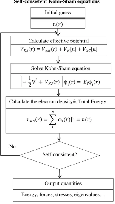
2.5.3. Kohn-Sham anstaz ... 42
2.5.4. The exchange-correlation energy ... 47
2.5.4.1. The Local Density Approximation ... 47
The Generalized Gradient Approximation ... 49
2.5.4.2. 2.5.5. Electronic structure of solids: Practical calculations ... 50
2.5.6. Equilibrium Position of Atoms: The Force Theorem ... 51
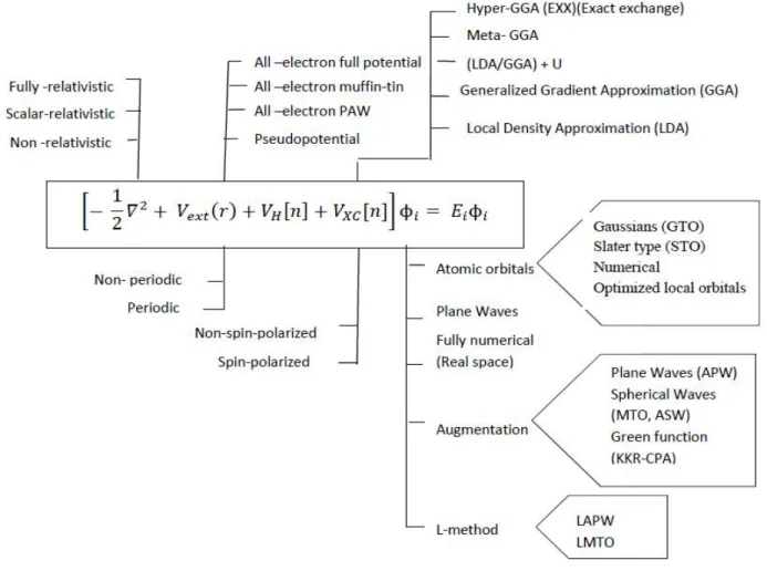
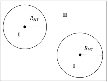
2.5.7. Electronic structure of solids: Basic Methods and Practical calculations ... 52
FPLO ... 57
2.5.4.3. WIEN 2K (FP- LAPW) ... 58
2.5.4.4. 2.6. Monte Carlo simulation ... 62
2.6.1. Introduction ... 62 2.6.2. Magnetic Models ... 64 Lattice Models ... 64 2.6.1.1. Spin Models ... 66 2.6.1.2. 2.6.3. The Monte Carlo Method basic concept: Importance Sampling... 67
2.6.4. Metropolis Algorithm ... 69
2.6.5. Measurement ... 70
XVII
Part III: Physical properties of 2D hexagonal nanostructured materials: A
theoretical study
3. Chapter 1: Preliminary view on Single Layer Materials: Models and Methods ... 74
3.1. Introduction ... 74
3.2. Computation methods ... 75
3.3. Results and discussions ... 76
3.4. Conclusion ... 82
4. Chapter 2: On Distance Variation Effects on Graphene Bilayers ... 83
4.1. Introduction ... 83
4.2. Models and method ... 84
4.3. Results and discussions ... 87
4.3.1. Vertical distance variation ... 88
4.3.2. Diagonal distance variation ... 91
4.4. Conclusion ... 94
5. Chapter 3: Interdistance Effects on Silicene and Germanene Like-bilayers ... 95
5.1. Introduction ... 95
5.2. Building models and method ... 96
5.3. Results and discussions ... 97
5.3.1. Bilayers of silicene ... 98
5.3.2. Bilayers of germanene ... 102
5.1. Conclusion ... 108
6. Chapter 4: Adsorption of Fe, Co and Ni on the Graphene with a Double Hexagonal Symmetry: Electronic and Magnetic properties ... 109
6.1. Introduction ... 109
6.2. Computational Method ... 112
6.3. Relaxation method ... 113
6.4. Results and discussions ... 113
6.5. Conclusion ... 122
7. Chapter 5: New Hexagonal Structure for C, Si and Ge Atoms... 123
7.1. Introduction ... 123
XVII
7.3. Results and Discussions ... 127
7.4. Conclusion ... 132
General Conclusion and Outlook ... 135
Outlook ... 138
Sufyan S.A. Naji General Introduction
1
General Introduction
Since the discovery of the graphene from bulk natural graphite by Novoselov et al. [1], the two dimensional materials (2DM) become the most promised research topics in condensed matter physics and related areas including high energy physics. [1], [2], [3], [4] [5]. [6], [7], [8], [9] [10], [11], [12].This discovery led to a revolution in research topics including the investigation of, the outstanding properties of such material, the possible applications and the other 2D layered materials. In fact, graphene has some fascinating physical properties that makes it extremely appealing for applications These properties include extraordinary high room-temperature electron mobility [13] , high Young’s modulus and intrinsic strength [14], extremely high thermal conductivity [5], an excellent optical transparence [15] , complete impermeability to any gases [16], highest current density at room temperature (a million times higher than copper) [17]. It has to be mentioned that, the Nobel Prize in Physics 2010 was awarded to Andre Geim and Konstantin Novoselov from the University of Manchester for groundbreaking experiments regarding the two-dimensional material graphene.
Furthermore, a special interest is to investigate the particular materials composed of atoms appearing in the fourth group of Mendeleev chemistry table [18], [19]. This includes only the graphene-like 2D buckled Nano sheets silicene and germanene .These counterparts of graphene, have evolved from theoretical predictions [18] to experimental observations [6] [12] [20], [21], only within a few years. Theoretical calculations have shown that they exhibit electronic characteristics similar to those of graphene [11].It has been shown that such honeycomb-structured models play crucial role placed in Nano-science and Nano-technology. Moreover, it has been suggested that, these structures could be considered as the most stable material systems used in the semiconductor electronic applications [5], [22], [23].
On the theoretical side, due to the continuous advances in computer technology, nowadays the computational modeling and simulation could be considered as a third stream together with pure theory and experiment to scientific investigation. They provide a modeling of physical phenomenon from a broad range of perspectives, from the electronic structure methods to the macroscopic end. The computational methods of different structures of materials and their
Sufyan S.A. Naji General Introduction
2
properties, in different scales, can be very valuable and useful for developing materials and their applications. As these methods offer acceptable accuracy in prediction of materials properties, they are widely used in the development of new materials and for interpretation of experimental results.
More precisely, the possibility to predict novel materials like, nano-systems and to calculate their basic chemical and physical properties is quite remarkable with falling back on the elementary interactions and the most accurate electronic structure methods for their simulation. Acutely, the Nobel Prize in chemistry 1998 was awarded, , in the field of electronic structure approaches, jointly to Walter Kohn for his work developing the foundations of the density functional theory and John Pople for his groundbreaking work on developing a quantum chemistry computer code for calculating the electronic structure of atoms and molecules.
It might be convenient now to remind that, the down-scaling of microelectronic devices associated with the increase of the hardware capacities involves technological challenges such as Moore’s law. On the other side, it has been found, recently, that, the systems based on the graphene physics are interesting for the electron-device community see refs. [24], [25] and references therein. In particular, the systems based on transistors have been extensively investigated and they are considered as an alternative option for the silicon electronic applications. However, one of the main challenges of graphene is its zero band gap energy, therefore, in order to use the graphene in semiconductor electronics, such as in transistors , the band gap should be opened [26] . In this context, the first goal of this thesis is to present our contribution to these activities by considering a new way for discussing the opening of the band gap energy using distance variation effects on two parallel sheets of the graphene placed in various stacking arrangements.
Moreover, the study of these intermediate configurations, describing the disorder in the bilayer of the graphene, should be interesting. It may occur during the production of samples and that it can influence quite strongly on the electronic properties. Effectively, such structures have been observed experimentally by STM on graphite surfaces [27], [28]. It has also been revealed experimentally that the Moiré patterns appear when the graphene plane is the considered cleaved graphite [29]. Therefore, the second goal of this thesis is, in the same chapter, to define a special
Sufyan S.A. Naji General Introduction
3
direction in which all possible intermediate arrangements between (AB) and (AA) configurations can be covered .The choice of this direction is motivated from the fact that this is the only direction that can produce the (AA) configuration starting from the (AB) one.
Another issue and as a bonus, the opening of the band gap energy using distance variation effects on two parallel sheets of the graphene is extend to the graphene counterparts like-bilayer; silicene and germanene.
Furthermore, many efforts have been devoted to study the interaction of the metal adatoms in the graphene-like models [30], [31], [32], [33], [34]. This interaction can be used for many potential applications including the building of the nano-magnetic materials. Precisely, the interaction of the magnetic atoms with the graphene like materials can produce half-metallic systems which have been considered as interesting tools for the spintronic device applications [35], [36], [37]. More precisely, several potential applications of spintronic could be spin field-effect transistor (spin-FET) [38], spin-light emitting diode (spin-LED) [39], magneto-resistive random access memory (MRAM) [40]. However, a lot of research still needs to be done to understand all the processes involved in this field. So, another main goal of this thesis is concerned with the theoretical investigation of the interaction between adatoms (Fe, Co, or Ni) and graphene with a double hexagonal symmetry, which might be useful for this kind of applications. Properties such as binding energies, magnetic moments, spin polarization, critical temperature and exchange mechanism will be examined with the density functional theory calculations and Monte Carlo simulations.
The last issue in this thesis is to examine, theoretically, a new hexagonal structure for monolayer C, Si and Ge atoms. This extended structure is based on a double hexagonal flat geometry which is associated with the two dimensional root system of the exceptional Lie algebra G2 and
motivated by several experimental observations [41], [42].
The organization of this thesis is as follows: Chapter 1 will present an introduction to the graphene, as one of the crystalline carbon allotropes, properties, counterparts, synthesis and applications.
Sufyan S.A. Naji General Introduction
4
Chapter 2 will focus on the needed background of the computational methods for the calculations that are performed in later chapters.
Chapter 3 will give a preliminary survey on the single layer of graphene, silicene and germanene.
Chapter 4 will deal with the opening of the band gap energy using distance variation effects on two parallel sheets of the graphene placed in various stacking arrangements.
Chapter 5 will treat, using distance variation effects, the opening of the band gap of silicene- and germanene-like bilayer.
Chapter 6 will investigate the electronic and magnetic properties of the adsorption of Fe, Co and Ni on the graphene with a double hexagonal symmetry.
Chapters 7 will examine, theoretically, a new hexagonal structure for flat monolayer C, Si and Ge atoms which is associated with the two dimensional root system of the exceptional Lie algebra G2.
Sufyan S.A. Naji Graphene: Basic Survey
5
1. Graphene: Basic Survey
1.1. Carbon bonding and allotropes:
Carbon is one of the most flexible elements in terms of the number of compounds. In fact, it forms the basis of all organic molecules, which makes it the most important element for life on our planet, and exists in over 95% of the known chemical compounds overall [43]. This strong capability is due to the types of bonds and the number of different bonding elements. Carbon, like the fourth group elements of Mendeleev table, has six electrons with the ground state atomic configuration is 1s2, 2s22p2. Two electrons form a closed 1s2 shell while the remaining four electrons are available to form covalent bonds. In order to get covalent bonds in the presence of some atoms, such as other carbon atoms, it should be excite one electron from the 2s to the third 2p orbital, as the energy difference between them is almost 4.2eV [44], providing four unpaired electrons that are able to form bonds. These four atomic orbitals can be mixed together to form four or three energetically equivalent hybrid orbitals. This process is called hybridization. The kind of this hybridization can be sp2 or sp3 hybridization. In the sp2 hybridization, two of the 2p-orbitals and one 2s-orbital take part in the hybridization process. This hybridization makes three energetically equivalent sp2-hybrid orbitals, which adopt a trigonal planar geometry with bond angles of and one unchanged p-orbital that sets at right angles to the plane of the hybrid orbitals. However, in the sp3 hybridization, the four orbital can be mixed together to form four energetically equivalent sp3-hybrid orbitals adopting a tetrahedral geometry with bond angles of 109°, as shown schematically in Figure 1.1 .
The crystalline carbon allotropes, i.e. those crystalline materials which entirely consist of carbon atoms, can be divided into two classes according to the type of bonds. Diamond or graphitic structures are formed, when all carbon atoms either have sp3-hybridization or sp2 -hybridization, respectively. It should be mentioned that, there is another class of non-crystalline carbon allotropes contains the amorphous carbons which consist of mixtures of sp2- and sp3 -hybridized carbon atoms.
Sufyan S.A. Naji Graphene: Basic Survey
6
Figure 1.1: schematic representation of sp2 (left) and sp3 hybridizations (right).
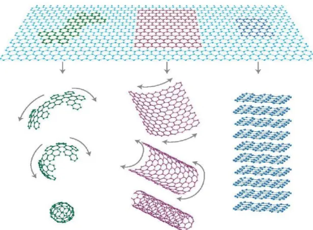
A schematic overview of these different crystalline carbon allotropes is given in Figure 1.2. These crystalline allotropes span all three spatial dimensions from 0D fullerene and carbon nano-flake, 1D carbon nanotubes and nanoribbons, 2D graphene to 3D graphite and diamond. These materials are briefly described in the following.
Sufyan S.A. Naji Graphene: Basic Survey
7
1.1.1. Diamond
Diamond is the most famous carbon allotrope, the highest thermal conductive and the strongest bulk materials. These exceptional properties are results from the strong covalent bonding between its atoms. In diamond, each atom has four bonding partners forming equivalent sp3-bonds at distance of 1.545 Å, leading to different crystal structures. Nearly all diamonds have the usual cubic structure but a very small percentage show a hexagonal structure related to wurtzite and these are called lonsdaleite. For pressures above , the cubic diamond is the thermodynamically stable form of carbon. Diamond is a slightly more compact structure; hence its density is greater than that of graphite. Like graphite, it is relatively unreactive but does burn in air at 600-800°C. All diamond materials are excellent insulators that characterized by an exceptional hardness and a large band gap giving them their transparent appearance. Such properties make them very useful for both industrial applications and jewelry.
1.1.2. Graphite
Graphite is the most stable carbon allotrope, under standard conditions, and the most common in nature consequently. At very high temperatures and pressures (roughly and ), it can be transformed into diamond. It is known for a long time as a writing material tools and lubricants to its unusual layered structure at the nano scale. As shown in Figure 1.2, the graphite structure consists of layers of covalently bonded carbon atoms which are held together by weak van der Waals interaction. The intra-layer bonding exceeds the interlayer bonding in strength by several orders of magnitude which can be demonstrated by the intra-layer bond length of as compared to for the interlayer bonds. In most graphite (α-graphite), these layers are arranged in as ABABAB... but in the less common form of graphite, β-form (rhombohedral), the stacking is ABCABCABC... although all the carbon-carbon distances remain the same as in the α-form.
Even though graphite is 3D in nature, it can often be regarded as a ( ) D material. Unlike diamond, graphite is an electrical conductor and due to the electrons and phonons can propagate much faster along the layers than from one layer to another, the thermal, electrical and other properties of graphite are highly anisotropic. The graphite forms of the heavier elements are not known and the structures of silicon, germanium, and tin are related to the diamond structure above.
Sufyan S.A. Naji Graphene: Basic Survey
8
1.1.3. Fullerene
Fullerene is a closed cage molecule builds up from carbon atoms, which was first discovered in 1985. Fullerenes have different forms, such as hollow sphere, ellipsoid and many other shapes. Spherical fullerenes are also called buckyballs like which consists of consists of
12 pentagons and 20 hexagons. From the structural point of view fullerenes are similar to graphite, with hexagonal carbon ring but they may also contain pentagonal or heptagonal rings. In the past two decades the discovery fullerenes attracted a lot of attention in physics, chemistry, mathematics, architecture and engineering. For their discovery of fullerene, Nobel Prize in Chemistry 1996 was awarded jointly to Robert . Curl Jr., Sir Harold W. Kroto and Richard E. Smalley.
1.1.4. Carbon nanotubes
Single-walled carbon nanotube is a one-dimensional (1D) form of carbon and it was discovered in 1991 by S. Iijima [45]. It can be thought of as rolled up monolayer sheet of graphene (see Figure 1.2 and Figure 1.4) and, consequently, many of their properties can be derived from those of graphene. These sheets are also rolled at specific and discrete ("chiral") angles, and the combination of the rolling angle and radius decides the nanotube properties; for example, whether the individual nanotube shell is a metal or semiconductor. Carbon nanotubes have unusual properties, which are valuable for the fields of materials science and technology. In particular, owing to their extraordinary thermal conductivity and mechanical and electrical properties, carbon nanotubes find applications as additives to various structural materials.
1.1.5. Carbon nanoribbons
Graphene nanoribbons have one-dimensional structures with hexagonal two dimensional carbon lattices, which are stripes of graphene with ultra-thin width ( ). Graphene nanoribbons can be divided into two kinds: Armchair and Zigzag and depending on this termination style, graphene nanoribbons present different electronic properties ranging from normal semiconductors to spin-polarized half metals, which open the possibility of graphene nanoribbons as electronic devices. In fact, Armchair graphene nanoribbons show semiconducting behaviors with a direct energy gap, while the zigzag graphene nanoribbons have been predicted to have a magnetic insulating ground state with ferromagnetic ordering at each zigzag edge, and
Sufyan S.A. Naji Graphene: Basic Survey
9
antiparallel spin orientation between the two edges. The importance of one-dimensional quantum confinement effect and edge states are crucial in determining its properties .Since graphene nanoribbons have large surface-volume ratio and special edge states, their properties can be also modified by many methods, such as doping and adsorption [46], [47] [48], [49], [50].
1.1.6. Carbon nano-flakes
Another zero-dimensional (0-D) form of graphene, which may be called graphene nano-flakes or graphene nano-dots. Graphene nano-nano-flakes have a great potential for a variety of applications especially in magnetic and electronic devices which differ from those of 2D and 1D graphene structures. These potential applications arise because graphene nano-flakes not only have edge states, but also corner states, and may also be cut into a much larger variety of different shapes which can play a very important role in determining their electronic and magnetic properties [47]. Besides these edges and corners, the effect of defects is also important and may introduce new properties such as magnetism. However, these defects often degrade the nano-flakes properties. Due to the finite size, defects can dominate, depending on defect size and density, the structure and its properties. Furthermore, functional groups attached to the graphene nano-flakes can also open new opportunities for technological applications including spintronic, sensors and transistors see [47] and references therein.
1.1.7. Graphene
Graphene is a two-dimensional (2D) form of crystalline carbon and it is the first perfect 2D materials with single-atom thickness arranged in a honeycomb lattice. In 2004, it is the first experimental isolation of graphene from bulk natural graphite by Noveselov et al [1]. This experiment led to a revolution in research including the investigation of the fascinating properties of such material and the possible applications. These fascinating properties including extremely high intrinsic electron mobility at room-temperature electron mobility > 1.0× cm2V−1s−1 [13] , highest current density at room temperature (a million times higher than copper) [17], extraordinary high thermal conductivity (about Wm−1K−1) [5], optical absorption of exactly πα ≈ 2.3% (in the infrared limit, where α is the fine structure constant) [15] , the strongest and the most stretchable known material with a Young’s modulus of 1TPa and intrinsic strength
Sufyan S.A. Naji Graphene: Basic Survey
10
of 130 GPa [14], complete impermeability to any gases [16] and others [51] . Due to these properties, graphene offers and promises a lot of different applications, such as nano-electronics, optical devices, sensors, composites, batteries, energy generation and hydrogen storage, [52], [53], [54], [25], [55], [56], [57], [58], [59], [60] and references therein. The Nobel Prize in Physics 2010 was awarded to Andre Geim and Konstantin Novoselov from the University of Manchester for groundbreaking experiments of the 2D material graphene.
Since the mid-30s of the past century, it was convinced, according to the theoretical works of Peierls [61], Landau [62] and Mermin and Wagner [63], [64],that, 2D crystals are thermodynamically unstable and strictly cannot exist at any finite temperature due to the thermal fluctuations that destroy the long range order leading to melt the 2D crystals. This thought was confirmed by experimental observations like the decreasing melting temperature for films with the decreasing thickness. Moreover the failure of creating thin films , since these films became unstable and tend to separate and clump up rather than form perfect layers, seemed to provide also strong support for this theory.
It came therefore as a big surprise when Novoselov, Geim et al. at Manchester University succeeded to isolate a stable single layer of carbon atoms and some other 2D materials in 2004. [1]. Currently the stability of graphene can be explained by postulating small out-of-plane corrugations (see Figure 1.3) due the anharmonic coupling between its bending and stretching modes [65], [66]. These corrugations have been observed on a lateral scale around 10 nm and are believed to suppress thermal vibrations [65]. An alternative explanation is found by considering the graphene layer is kept in its metastable state by van der Waals interaction with a supporting substrate and the strong intra-layer bonds which prevent the defects formation.
Moreover, the graphene, can form the basis of all these other graphitic allotropes (see Figure 1.4) graphite, which is a three-dimensional crystal consisting of relatively weakly coupled graphene layers; nanotubes, which may be represented as scrolls of graphene; and buckyballs, spherical molecules made from graphene with some hexagonal rings replaced by pentagonal rings.
In a graphene layer the carbon atoms are distributed at the edges of regular hexagons (see Figure 1.5 (a)). This structure is often called a honeycomb lattice. However, the honeycomb lattice is not a Bravais lattice and from a crystallographic point of view, it has to be described by
Sufyan S.A. Naji Graphene: Basic Survey
11
a triangular lattice with two atoms per unit cell. These two atoms are often referred to as A and B atoms. The unit cell of the lattice is a rhomboid defined by the vectors:
(√ ) (√ ) [1.1]
Each carbon atom (A or B) is covalently bonded by σ-bond to its three nearest neighbors and the separation distance between type A (B) and the nearest type B (A) atoms is approximately 1.42 Å and given by :
√
[1.2] The reciprocal lattice of graphene is also a hexagonal lattice (see Figure 1.5 (b)) that can be defined by the reciprocal vectors as:
( √ ) ( √ ) [1.3]
with √ . The first Brillouin zone (BZ) has sides length √
is shown by the shaded area in Figure 1.5 (b). The Γ-point is at the center of this zone, and the vectors describing the location of the special high-symmetric points with respect to the zone center are given by:
( √ ) ( √ ) [1.4]
Sufyan S.A. Naji Graphene: Basic Survey
12
Figure 1.3: Simulated model for the crumpling of a graphene monolayer in the third dimension. (Figure from Ref. [3] (journal cover).)
Figure 1.4: Graphene forms the basis of the other graphitic carbon allotropes; from left to right: fullerene, carbon nanotube, and graphite. (Taken from ref [2].)
Sufyan S.A. Naji Graphene: Basic Survey
13
Figure 1.5: (a) The honeycomb lattice of graphene. The unit cell in gray contains two atoms denoted as A and B (b) the reciprocal lattice with the hexagonal first BZ shown in green and the second BZ shown in yellow. The special high-symmetry points labeled as , , and K located at the center, midpoint of the side, and corner of the hexagon respectively.
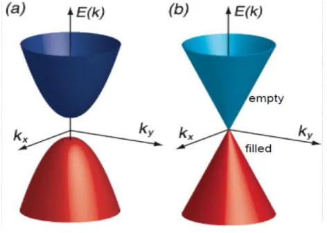
Figure 1.6 : Schematic view of band structure for (a) ordinary semiconductors or insulators (b) graphene around K-point.
Sufyan S.A. Naji Graphene: Basic Survey
14
In 1947, the first electronic structures calculations for a single graphite layer obtained by P. R. Wallace [67] in the framework of a simple tight-binding model. Further this model was developed by McClure in1957 [68] and by Slonczewski and Weiss in1958 [69]. The electronic structures of graphene is consist from the σ-states that form occupied and empty bands with a huge gap, whereas π states form a single band, with a conical self-crossing point in K. This conical point is a characteristic of the peculiar electronic structure of graphene and the origin of its unique electronic properties. In particular, near the so-called Dirac points the system has a linear energy dispersion i.e.
[1.5]
Where and are momentum and Fermi velocity respectively. Linear dispersion behavior indicates that the charge carriers near Dirac point become like massless fermionic fields satisfying the relativistic Dirac-like equation [23]. On -points, the usual graphene material is considered as a gapless semi-conductor see Figure 1.6.
In 1984, G.W. Semenoff [70] showed the possibility of a (2+1)D quantum electrodynamics analog with graphene as a condensed matter system by a Hamiltonian consists of two decoupled copies of the Dirac equation at low energy, which are related by time reversal. The existence of such Dirac fermions in single layer graphene confirmed finally in 2005 by two papers appeared in Nature [71], [72] . The charge carriers of graphene and its unique electronic structure leads to a number of interesting physical effects, such as the minimal electrical conductivity, anomalous quantum Hall effect, Klein tunneling, the universal optical conductivity and the strong nonlinear electromagnetic response [53], [73].
1.2. Graphene Counterparts:
Since the discovery of the graphene from bulk natural graphite by Novoselov et al [1], the two dimensional materials (2DM) become the most promised research topics in condensed matter physics and related areas including high energy physics. This discovery led to an explosion in research topics including the investigation of, the outstanding properties of such material, the possible applications and the other 2D layered materials [1], [2], [3], [4] [5]. [6], [7], [8], [9] [10],
Sufyan S.A. Naji Graphene: Basic Survey
15
[11], [12]. These 2D layered materials including graphan, fluorographene, boron-nitride, transition metal oxides, metal chalcogenides and other 2D materials have gained huge interest for their particular electronic structure ranging from insulator to metal to superconductor. A large variety of layered materials with weak van der Waals-like inter-layer bonds and strong intra-layer bonds exists which could potentially be exfoliated into 2D materials. These have different properties such as superconductivity [74], topological insulator effect [75], [76] , and thermoelectricity [77] [41]. Furthermore, a special interest is to investigate the particular materials composed of atoms appearing in the fourth group of Mendeleev chemistry table [18], [19]. This includes only the graphene-like 2D buckled Nano sheets silicene and germanene. These graphene counterparts have evolved from theoretical predictions [18] to experimental observations [6], [12], [20], [21], only with a few years. It has been shown that such honeycomb-structured models play crucial role placed in Nano-science and Nano-technology. Moreover, it has been suggested that, they could be considered as the most stable material systems used in the semiconductor electronic applications [5], [22], [23].
More precisely, there has been a great interest in studying the silicene since it involves properties similar to those of the graphene [5], [6], [10] . For this reason, the silicene, which is a monolayer of the silicon atoms forming a 2D honeycomb lattice, can be also viewed as an alternative potential candidate for nanotechnology applications. This material has been synthesized and modeled using different approaches [78], [79], [80], [81], [82], [83], [84].
Recently, the electronic properties of two-dimensional hexagonal materials of germanium and numerical calculations on the ground state properties of germanene have been also done using first-principles method [85], [86], [87], [88], [89]. In particular, it has been found that the buckled germanene is more stable than the planar one involving an electronic structure similar to graphene with linear energy dispersion around the K point [86].More recently, the 2D buckled and nearly flat germanene sheets have been, also, fabricated with two different surface substrates [20], [21].
In the present thesis, I focus my studied basically on graphene and as extension of some works on silicene and germane.
Sufyan S.A. Naji Graphene: Basic Survey
16
Figure 1.7: Several methods of mass-production of graphene, which allow a wide choice in terms of size, quality and price for any particular application.(Taken from ref. [59].)
Figure 1.8: Graphene films. (A) Photograph (in normal white light) of a relatively large multilayer graphene flake with thickness around 3 nm on top of an oxidized Si wafer. (B) Atomic force microscope (AFM) image of 2 μm by 2 μm area of this flake near its edge. Colors: dark brown, SiO2 surface; orange,
3 nm height above the SiO2 surface. (C) AFM image of single-layer graphene. Colors: dark brown, SiO2
surface; brown-red (central area), 0.8 nm height; yellow-brown (bottom left), 1.2 nm; orange (top left), 2.5 nm. Notice the folded part of the film near the bottom, which exhibits a differential height around of 0.4 nm. (D) Scanning electron microscope image of one of the experimental devices prepared from FLG. (E) Schematic view of the device in (D).( Taken from ref. [1]).
Sufyan S.A. Naji Graphene: Basic Survey
17
1.3. Graphene: preparation techniques
Up to date, graphene and its systems with varying number of layers, dimensions, shapes and quality can be synthesized by different techniques (see Figure 1.7). These techniques include exfoliation of graphite, chemical vapor deposition, arc-discharge method, epitaxial growth on electrically insulating surfaces such as SiC, chemical reduction of graphite oxide and graphite intercalation compounds and others. Generally, these preparation techniques can be distinguished into two major classes. First, the top-down approaches that start from graphite and in many ways try to extract few layer graphene and ultimately monolayers. Secondly, the bottom-up approaches that the graphene can be grown directly on a substrate surface. Techniques of the first and second classes are called, respectively, exfoliation and synthesis methods. Here, I will briefly present some of the most important preparation techniques. For more details on these techniques and the others can be found in [52], [90] , [59] and references therein.
1.3.1. Mechanical Exfoliation
The first single layer of graphene was prepared using the micromechanical exfoliation or, simply, what so-called Scotch tape method from highly ordered pyrolytic graphite (HOPG) in 2004 by Novoselov and Geim [1]. In this technique an adhesive tape was used to repeatedly to peel off flakes of multilayered HOPG layer-by-layer until the multilayer is cleaved into various flakes of few layer graphene and ultimately single layers. After this, the tape is pressed on a Si/SiO2 substrate in order to attach the graphene samples.
Afterwards, thick flakes are, mostly, removed using ultrasound cleaning propanol while the thin ones ( ) are, strongly deposited to the substrate due to van der Waals interaction [1]. These few layer graphene are identified by the contrast difference in an optical microscope. Finally, in order to confirm the optical microscope observation, more accurate characterization techniques such as atomic force microscopy (AFM), scanning electron microscope (SEM) and Raman spectroscopy can be used as shown in Figure 1.8. This technique can generate few and single layer graphene samples with dimension up to . Besides its historical importance and simple concept, this technique is still extremely valuable especially in fundamental research due to the excellent sample quality with almost no defects that cannot be produced by any recent
Sufyan S.A. Naji Graphene: Basic Survey
18
technique. However, this method is limited to small size production and cannot be used for industrial applications that require a large- scale production of graphene [59].
1.3.2. Chemical Vapor Deposition
In the chemical vapor deposition (CVD) technique, single layer of graphene is prepared, more conveniently, by decomposing a variety of hydrocarbons such as methane, ethylene, acetylene and benzene on films or sheets of different transition metal substrates such as Ni, Cu, Co and Ru. This transition metal can be used as both catalyst and substrate to grow the graphene layer and the number of layers can be varied with the hydrocarbon and reaction parameters. Using CVD method, large-area uniform polycrystalline graphene films on copper foils and films have been produced showing great promise for many industrial applications(see Figure 1.9 (a)) [91] . The independent of growth time for graphene monolayer is confirmed by Raman spectroscopy and SEM imaging. The production of square meters of graphene has already been achieved, in spite of the fact that the whole process typically needs transfer from the copper support to a dielectric surface or other substrate of interest [59], [92].
It has been demonstrated, recently, that, the CVD on copper with a similar process but modified growth conditions can be used as technique to produce uniform bilayer graphene [93]. Despite the cons of this method like, the grain boundaries, inclusions of thicker layers and the presence of defects, such produced films can readily be used in transparent conductive coating applications including touch screens.
Several issues associated with the doping level, gaining control of the grain size, number of layers, and the ripples need to be resolved. Finally, in order to minimize the damage to graphene, the transfer process should be also optimized. Using plasma-enhanced CVD or other methods, the future aim would be the improvement of graphene growth on arbitrary surfaces and/or at low temperature with a minimal number of defects.
1.1. Applications of Graphene
The Fascinating properties of graphene make this material extremely appealing for different applications. In the past few years, graphene offers and promises a lot of different applications, such as nano-electronics, optical devices, sensors, water desalination, bio applications, metrology
Sufyan S.A. Naji Graphene: Basic Survey
19
composites, coating, batteries, flexible transparent electrodes, spintronic energy and hydrogen storage, [52], [53], [54], [25], [55], [56], [57], [58], [59] , [60] and references there in. I will mention, in the next sections, some areas for existing and future applications.
Figure 1.9 : (a) A large continuous display based on few-layer graphene deposited on a polymer substrate, fabricated by Samsung company (Taken from Ref. [91]). (b) A flexible graphene screen.
1.1.1. Flexible transparent electrodes
Transparent conducting (TCs) materials are widely used as transparent electrodes in several optoelectronic and photovoltaic applications. These applications include liquid crystal displays (LCD), (organic) light-emitting diodes ((O) LEDs) and solar cells devices. Generally, the recent technology used Indium Tin Oxide (ITO) like an electrode in such applications. However, the ITO suffers from the scarcity, high cost of indium (In) and the brittle nature of ITO that greatly restrict its application.
This situation led to the search of an alternating non-toxic and abundant TCO material with optical, electrical and mechanical properties comparable or better to those of the current ITO materials. Due to its high chemical and mechanical stability, unique mechanical flexibility, excellent optical transparency in the visual spectrum, atomic layer thickness and the low sheet resistivity (see Figure 1.10), Graphene based on TCs has been suggested, recently, as an ideal


![Table 2.1: Top ten algorithms of the 20 th century [118], [119].](https://thumb-eu.123doks.com/thumbv2/123doknet/2184057.10703/49.918.108.813.603.974/table-algorithms-th-century.webp)
![Figure 2.2: An extension of Moore's law from integrated circuits to earlier transistors, vacuum tubes, relays and electromechanical computers [121]](https://thumb-eu.123doks.com/thumbv2/123doknet/2184057.10703/50.918.134.786.513.945/figure-extension-integrated-circuits-earlier-transistors-electromechanical-computers.webp)