Graphene : FET and metal contact modeling – Graphène : modélisation du FET et du contact métallique
129
0
0
Texte intégral
Figure
![Figure 2.1: Quality vs. Cost for graphene production. Adapted from [ 21 ].](https://thumb-eu.123doks.com/thumbv2/123doknet/2181464.10530/16.893.242.599.125.442/figure-quality-vs-cost-graphene-production-adapted.webp)


+7
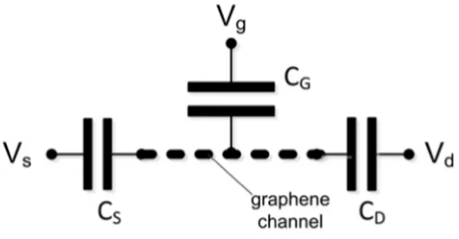
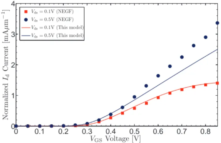
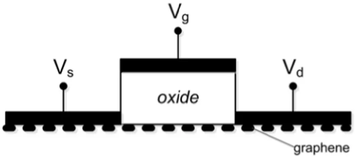
![Figure 3.7: (a) The cross-section of the large-area graphene FET of [ 14 ]. Graphene is the black thick dotted line under contacts and top-gate oxide](https://thumb-eu.123doks.com/thumbv2/123doknet/2181464.10530/59.893.296.660.178.560/figure-cross-section-large-graphene-graphene-dotted-contacts.webp)
Documents relatifs
