UNIVERSITÉ DE MONTRÉAL
ELECTROLYTE GATED METAL OXIDE TRANSISTORS
IRINA VALITOVA
DÉPARTEMENT DE GÉNIE CHIMIQUE ÉCOLE POLYTECHNIQUE DE MONTRÉAL
THÈSE PRÉSENTÉE EN VUE DE L’OBTENTION DU DIPLÔME DE PHILOSOPHIAE DOCTOR
(GÉNIE MÉTALLURGIQUE) AVRIL 2017
ÉCOLE POLYTECHNIQUE DE MONTRÉAL
Cette thèse intitulée:
ELECTROLYTE GATED METAL OXIDE TRANSISTORS
présentée par : VALITOVA Irina
en vue de l’obtention du diplôme de : Philosophiae Doctor a été dûment acceptée par le jury d’examen constitué de : M. KÉNA-COHEN Stéphane, Ph. D., président
M. CICOIRA Fabio, Ph. D., membre et directeur de recherche M. MOUTANABBIR Oussama, Ph. D., membre
ACKNOWLEDGEMENTS
I would like to express my deep gratitude to Professor Fabio Cicoira, my research supervisor, for his scientific guidance and the opportunity to get so vast experience; for his enthusiastic encouragement and useful critiques of this research work. My grateful thanks are also extended to Professor Clara Santato for her valuable advices and discussions, for the opportunity to work in her lab. I would like to thank our collaborator Professor Dr Francesca Soavi (Università di Bologna) for her advices in electrochemistry.
I am grateful for the funding provided by the Fonds de recherche du Québec - Nature et technologies (FRQNT) through a PhD scholarship and CMC Microsystems for microfabrication grants through programs MNT Financial Assistance and Solutions. My special gratitude goes to Christophe Clément, Yves Drolet, Alireza Mesgar, Josianne Lefebvre, Marie-Hélène Bernier, Francis Boutet, Daniel Pilon, Nicole MacDonald and Marta Maria Natile for their technical assistance during these years.
Also I would like to acknowledge the people I worked with, my colleagues and friends, Prajwal, Zhihui, Jonathan, Dilek, Olga, Fanny, Shiming, Xiang, Gaia, Guido, Tian, Eduardo, Xu, Elizabeth, Hao, Julia, Francis, Frédéric, Colleen, Tania, Dominic, Sampath, Gabriel, Mengjiao, Alex, Xinhe, Xiaojie, Shalin and Tom that were working along with me in labs and offices for all their help, support, guidance and just enjoyable quality of time during and in between my research. Thank you all very much. It was a great pleasure to work side-by-side with you!
I would like to thank my committee members, Profs. Stéphane Kena-Cohen, Oussama Moutanabbir, Michael Hilke, Antoniol Giuliano for volunteering their time to read this thesis and hear my defense and to make their valuable comments.
Finally, through all this I have had the unflagging support of my husband, who was “only” doing all housework and taking care of our kids all this time.
RÉSUMÉ
L’invention du transistor a significativement affectée le progrès technique et scientifique de notre société. Depuis plus de 50 ans, les transistors sont utilisés comme composants actifs dans les circuits électroniques, pour réaliser des amplificateurs ou des interrupteurs par exemple. La plus fascinante des directions futures pour le développement des transistors consiste en leur utilisation dans des dispositifs électroniques flexibles, légers et biocompatibles.
Les oxydes métalliques semi-conducteurs ont été intensivement étudiés au cours des dernières décennies pour des applications dans les transistors, du fait de la grande mobilité de leurs porteurs de charges (∼1– 100 cm2V-1s-1), de leur importante transparence optique, de leur
stabilité chimique ainsi que de leur faible coût de fabrication. Les oxydes métalliques sont divisés entre les oxydes de transition et ceux post-transition, dépendamment des métaux, qui possèdent différentes configurations électroniques et donc différentes conductivités.
Dans cette thèse, nous allons nous concentrer sur les deux principaux représentants des oxydes métalliques de transition et post-transition, i.e., le TiO2 et le SnO2, utilisés comme matériaux de
canal dans des transistors utilisant un électrolyte comme diélectrique à la grille. Le TiO2 et le
SnO2 sont abondants et biointégrables, possèdent une large bande interdite (3-4 eV), et peuvent
être utilisés comme canal de transistor pour de nombreuses applications différentes.
Remplacer le diélectrique conventionnel dans les transistors à couche minces par un électrolyte donne l’opportunité de décroître le voltage auquel le transistor est opéré du fait de la haute capacitance de la double couche électrique (autour de 10 µF/cm2) qui se forme à l’interface entre l’électrolyte et le semi-conducteur. Cette capacitance élevée permet l’accumulation d’une importante densité de porteurs de charges dans le canal et rend donc possible la transition entre un état isolant et un état semi-conducteur voire métallique. Les transistors utilisant un électrolyte comme diélectrique à la grille (EGTs) peuvent être employés comme éléments de matrice active pour les écrans à faible puissance ou encore intégrés dans des textiles ou d’autres matériaux flexibles. Les EGTs peuvent aussi être utilisés dans d'autres applications prometteuses que sont telles les capteurs chimiques ou biologiques, du fait de leur haute sensibilité aux ions et de leur compatibilité avec les électrolytes aqueux.
Le cœur de cette thèse est dévoué à une meilleure compréhension des mécanismes d’opération d’une importante classe de transistors à couche minces, i.e. les transistors à oxydes métalliques
utilisant un électrolyte comme diélectrique à la grille, afin d’optimiser leurs performances et de développer des agencements géométriques pour permettre d’obtenir des transistors à haute performance. Les EGTs consistent en un canal en oxyde métallique et en une électrode de grille en contact avec un électrolyte. L’application d’un voltage à la grille entraîne la formation d’une double couche électrique au niveau de l’interface entre le canal et l’électrolyte, qui permet de moduler la densité des porteurs de charges dans le canal. Les mécanismes de dopage et la modulation de la densité des porteurs de charges dans les EGTs ont été étudiés par caractérisation électrique des transistors, par voltammétrie cyclique (CV) ainsi que par spectroscopie d’impédance électrochimique.
Des transistors SnO2 et TiO2 utilisant des liquides ioniques à la grille ont été fabriqués sur des
substrats en silicone. Une méthode de gravure non conventionnelle utilisant le parylène a été utilisée pour étudier le rôle joué par l’extension des interfaces électrolyte/semi-conducteur et électrode/semi-conducteur sur le dopage ainsi que sur les processus de transport des porteurs de charges. Le chevauchement entre les électrodes métalliques et le semi-conducteur, qui est en contact avec l’électrolyte, affecte le processus d’injection des charges. La gravure a entraîné l’augmentation de la densité des porteurs de charges d’un à deux ordres de magnitude dans les deux oxydes métalliques. De plus, les EGTs à SnO2 ont été fabriqués sur des substrats flexibles
en polyimide. Les transistors EGTs à SnO2 flexibles possèdent de bonnes propriétés électriques
lorsqu’ils sont pliés selon différents rayons de courbure et ils pourraient posséder un fort potentiel pour des applications dans le domaine de l’électronique flexible.
Les effets de la structure et de la morphologie des semi-conducteurs sur les performances des transistors ont été étudiés. Dans ce but, des films de TiO2 poreux à très forte densité ont été
fabriqués par traitement à partir d’une solution ainsi que par évaporation par faisceau d’électrons. Les EGTs à TiO2 faits par évaporation possédaient un courant plus élevé ainsi qu’un ratio on/off
plus haut du fait d’une meilleure qualité de la structure. Les effets des gros cations [EMIM] et des petits cations Li+ sur les mécanismes de dopage ont été étudiés en utilisant deux électrolytes [EMIM][TFSI] et [EMIM][TFSI] mélangé avec un sel de lithium. Les relativement gros cations [EMIM] ne peuvent pas pénétrer à l’intérieur du maillage cristallin du TiO2. L’intercalation de
petits cations comme le Li+ a été rendue possible à la fois dans les films denses et dans les films mésoporeux de TiO2 par réduction de la vitesse de balayage dans les mesures courant/voltage.
Les mécanismes de transport des charges des transistors utilisant un électrolyte comme diélectrique à la grille ont été étudiés et une corrélation entre la capacitance de la double couche, la densité des porteurs de charges, la mobilité des électrons, la tension seuil et le ratio on/off a été démontrée. Nous pensons que nos transistors à oxydes métalliques utilisant un électrolyte comme diélectrique à la grille sont prometteurs pour de l’électronique flexible, produite sur de grandes surfaces et à faible coût.
ABSTRACT
The invention of the transistor has significantly affected the technological and scientific progress of our society. For over 50 years, transistors have been used as the active components, such as amplifiers or switches, in electronic circuits. The most fascinating future direction for transistor development is towards flexible, lightweight and biocompatible electronics.
Metal oxide semiconductors have been intensively investigated over the past decades for transistor applications, due to their high charge carrier mobility (∼1– 100 cm2V-1s-1), high optical
transparency, chemical stability and low-manufacturing cost. Metal oxides are divided into transition and post transition oxides, depending on the metals, which possess different electron configurations and, accordingly, different conductivity.
In this Thesis we focus on two main representatives of transition and post transition metal oxides, i.e., TiO2 and SnO2, as the channel materials in electrolyte gated transistors. TiO2 and SnO2 are
abundant and bio friendly, with high band gap (3-4 eV) and can be utilized as transistor channel for many different applications.
Replacing the conventional dielectric in thin film transistors with electrolyte gives the opportunity to decrease the transistor operating voltage due to the high capacitance of the electrical double layer (around 10 µF/cm2) that form at the electrolyte/semiconductor interface. This high capacitance allows accumulation of high charge carrier density in the channel thus making possible a transition from an insulating state to semiconducting or metallic one. Electrolyte gated transistors (EGTs) can be utilized as backplanes for low powered displays and integrated into textiles or flexible materials. Other exciting applications of EGTs are chemical sensors or biosensors, due to the high sensitivity to ions and compatibility with aqueous electrolytes.
The core of this thesis is devoted to a better understanding of the operational mechanisms of an important class of thin film transistors, i.e. electrolyte gated metal oxide transistors, to optimize their performance and to develop the appropriate device geometry for high performance transistors. EGTs consist of metal oxide channel and a gate electrode in contact with an electrolyte. The application of a gate electrical bias leads to the formation of an electrical double layer at the channel/electrolyte interface, which permits to modulate the charge carrier density in
the channel. The doping mechanisms and the charge carrier density modulation in EGTs were investigated by transistor electrical characterization, cyclic voltammetry (CV) and electrochemical impedance spectroscopy.
Ionic liquid gated SnO2 and TiO2 transistors were fabricated on silicon substrates. Parylene
patterning was utilized to investigate the role played by the extension of the electrolyte/semiconductor and electrode/semiconductor interfaces on the doping and charge carrier transport processes. The overlap between the metal electrodes and the semiconductor, which is in contact with the electrolyte, affects the charge injection process. By patterning the charge carrier density was increased on one or two order of magnitude in both metal oxide materials. Moreover, SnO2 EGTs were fabricated on flexible polyimide substrate. EGT SnO2
flexible transistors possessed good electrical properties under bending at different radius and could have high potential in flexible electronics.
The effect of structure and morphology of semiconductors on transistor performance was demonstrated. For this purpose, porous and highly dense films of TiO2 were fabricated by
solution processing and by electron beam evaporation. Evaporated TiO2 EGT showed higher
current and higher on/off ratio due to better structural quality. The effect of big [EMIM] and small Li+ cation on doping mechanisms was investigated by using two electrolytes [EMIM][TFSI] and [EMIM][TFSI] mixed with a lithium salt. The relatively large [EMIM] cation cannot enter the crystal lattice of TiO2. The intercalation of small cation such as Li+ was possible
both in mesoporous and dense TiO2 films by decreasing the sweeping rate in current / voltage
measurements.
The charge transport mechanism of electrolyte gated transistors was investigated and a correlation between capacitance of the double layer, charge carrier density, electron mobility, threshold voltage and on/off ratio was demonstrated. We believe that our electrolyte gated metal oxide transistors are promising for low cost, flexible and large area electronics.
TABLE OF CONTENTS
ACKNOWLEDGEMENTS ... III RÉSUMÉ ... IV ABSTRACT ... VII TABLE OF CONTENTS………...IX LIST OF TABLES ... XIII LIST OF FIGURES ... XIV LIST OF SYMBOLS AND ABBREVIATIONS ... XIX LIST OF APPENDICES ... XXIII
CHAPTER 1 INTRODUCTION ... 1
1.1 History of transistors ... 1
1.2 Thin film transistors ... 2
1.2.1 Working principle of thin film transistors ... 3
1.2.2 Main characteristics of thin film transistors ... 5
1.2.3 Thin film transistor configurations ... 7
1.2.4 The contact resistance and overlap capacitance ... 8
1.3 Electrolyte gated thin film transistors ... 9
1.4 Metal oxides (TiO2 and SnO2) as semiconductors ... 11
1.5 Problem identification ... 14
1.6 General Objectives ... 15
1.7 Motivation ... 15
1.8 Specific objectives ... 15
1.9 Organization of the work ... 16
2.1 Vapor processed thin film transistors ... 18
2.2 Solution processed thin film transistors ... 21
2.2.1 Reduction of the fabrication temperature ... 22
2.2.2 Role of dopant ... 24
2.3 Electrolyte gated thin film transistors ... 26
CHAPTER 3 ARTICLE 1 : TIN DIOXIDE ELECTROLYTE-GATED TRANSISTORS WORKING IN DEPLETION AND ENHANCEMENT MODE ... 35
3.1 Authors ... 35
3.2 Abstract ... 35
3.3 Introduction ... 36
3.4 Results and discussion. ... 37
3.4.1 Transistor fabrication and film characterization ... 37
3.4.2 Electrical characterization of SnO2 transistors ... 39
3.4.3 Electrochemical characterization of SnO2 films ... 43
3.4.4 Electrical characteristics under mechanical deformations ... 44
3.5 Conclusion ... 45
3.6 Materials and methods ... 46
3.6.1 Processing of SnO2 ... 46
3.6.2 Flexible transistor fabrication ... 46
3.6.3 Purification of the ionic liquid. ... 46
3.6.4 Fabrication of the activated carbon (AC) electrodes. ... 46
3.6.5 Morphology and structure of SnO2 films. ... 47
3.6.6 Surface area measurements. ... 47
3.6.7 Transistor and electrochemical characterization. ... 47
CHAPTER 4 ARTICLE 2: PHOTOLITHOGRAPHICALLY PATTERNED TIO2 FILMS FOR
ELECTROLYTE-GATED TRANSISTORS ... 48
4.1 Authors ... 48
4.2 Abstract ... 48
4.3 Introduction ... 49
4.4 Results and discussion ... 51
4.4.1 Patterning and Fabrication of the Devices ... 51
4.4.2 Electrochemical characterization of TiO2 films ... 54
4.4.3 TiO2 transistors and role of patterning ... 56
4.5 Conclusion ... 59
4.6 Experimental ... 60
4.6.1 Processing of TiO2 ... 60
4.6.2 Purification of the ionic liquid ... 60
4.6.3 Device Fabrication ... 60
4.6.4 Fabrication of the activated carbon (AC) electrodes. ... 61
4.6.5 Morphology and structure of TiO2 films. ... 61
4.6.6 Surface area measurements. ... 61
4.6.7 Transistor and electrochemical characterization. ... 62
4.7 Acknowledgments ... 62
CHAPTER 5 CHARGE CARRIER DENSITY MODULATION IN DENSELY PACKED AND POROUS POLYCRYSTALLINE TIO2 FILMS BY ELECTROLYTE GATING ... 63
5.1 Abstract ... 63
5.2 Introduction ... 63
5.3 Experiments and methods ... 65
5.3.2 Electrolyte preparation ... 65
5.3.3 Fabrication of the activated carbon (AC) electrodes ... 65
5.3.4 Device Fabrication ... 66
5.3.5 Morphology and structure of TiO2 films ... 66
5.3.6 Transistor and electrochemical characterization ... 66
5.4 Results and Discussion ... 66
5.5 Conclusion ... 75
CHAPTER 6 GENERAL DISCUSSION ... 77
CHAPTER 7 CONCLUSION AND RECOMMENDATIONS ... 79
BIBLIOGRAPHY ... 81
LIST OF TABLES
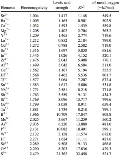
Table 2-1: Lewis acid strength of elements and their metal-oxide bonding strength. Reprinted with permission from [91]. Copyright 2014 Cambridge University Press. ... 25 Table 2-2 The electrical characteristics of some main metal oxide transistors. ... 33
LIST OF FIGURES
Figure 1-1: Schematic illustration of operating regimes of field effect transistors: (a) linear regime; (b) saturation regime at pinch-off; (c) corresponding current voltage characteristics. ... 4 Figure 1-2: Schematic illustration of thin film transistor configurations: bottom contacts - bottom gate (a, BC-BG), bottom contacts - top gate (b, BC-TG), top contacts - bottom gate (c, TC-BG) and top contacts - top gate (d, TC-TG). ... 7 Figure 1-3:Schematic illustration of an electrolyte gated thin film transistors operating in field effect (a) and electrochemical mode (b). ... 10 Figure 1-4: Example of the Bode plot (θ-f) in Pt/IL/Pt structure. Inset: equivalent electric circuit, two resistor-capacitor (RC) circuits in series. (b) The Bode plot of ZnO EDL transistor. I: bulk IL capacitive region. II: electrostatic EDL capacitive region; III: electrochemical pseudocapacitive region. Reprinted with permission from [58]. Copyright 2010 American Chemical Society. ... 11 Figure 1-5: Schematic illustration for the carrier transport paths in crystalline and amorphous covalent semiconductors and post transition MeOs. Reprinted with permission from[60] © Nature Publishing Group, 2004. ... 12 Figure 1-6:The crystalline structures structures and Brillouin zones of rutile D4h14 and anatase D4h19. Reprinted with permission from [61]. © AIP Publishing LLC, 2013. ... 14 Figure 1-7:Electronic structures structures of r- SnO2, r- TiO2, a- SnO2, and a- TiO2 along two
main symmetry directions (100) _|_ and (001) ||. Reprinted with permission from [61]. © AIP Publishing LLC, 2013. ... 14 Figure 2-1: (a) Schematic illustration of ZnO transistor; (b) transfer and (c) output characteristics of this transistor without passivation layer. Reprinted with permission from [72]. Copyright © 2015 American Chemical Society ... 19 Figure 2-2: Structure of InGaO3(ZnO)5. (A) Schematic illustration of the crystal structure. A
InGaO3(ZnO)5 thin film grown by reactive solid-phase epitaxy. Reprinted with permission
from [73]. Copyright 2003 The American Association for the Advancement of Science ... 20 Figure 2-3: Schematic illustration of the solution process for oxide TFTs: (a) Oxide solution was synthesized using metal precursors in solvent. (b) The synthesized oxide solution can be deposited on a substrate by various methods such as spin-coating, printing. (c) The oxide thin film was pre-annealed to remove the solvent and (d) post-annealed to develop an active layer. (e) The bottom-gate top-contact TFT structure was fabricated using solution process. (f ) The entire chemical reactions in the oxide solution. Reprinted with permission from [81]. Copyright 2014. ... 22 Figure 2-4: Thermogravimetric analysis of different IZO precursors. Reprinted with permission from [81]. Copyright 2010 Creative Commons CC-BY license. ... 23 Figure 2-5: a) Schematic illustration and optical image of a van der Pauw ion‐gel‐
([EMI][TFSI]+PS‐PMMA‐PS)‐gated printed In2O3 TFT; b) Electron density from Hall
effect (nHall), and from displacement current (nFET) versus VG. c) Hall mobility (µHall) versus
VG; nHall is labeled for each point. Reprinted with permission from [92]. Copyright 2017
John Wiley and Sons. ... 27 Figure 2-6: Schematic of the device to test for long range effects in oxide thin films away from the area being charged. The gate was a platinum mesh connected to a DC power supply. The spacing of voltage contacts was 300 µm for all devices. Reprinted with permission from [96]. Copyright 2011 American Chemical Society. ... 27 Figure 2-7: Optical images of a typical in-plane In2O3 transistor. (a) Patterned (with e-beam
lithography) ITO electrodes and a printed drop of In2O3 nanoink. (b) The optical image of
the same device after printing the electrolyte. (c) A schematic illustration of the device. Reprinted with permission from [96]. Copyright 2011 American Chemical Society. ... 28 Figure 2-8: Schematic diagram of a flexible IZO-based neuromorphic transistor with multiple
in-plane gate electrodes. Reprinted with permission from [75]. Copyright 2015 Creative Commons CC-BY license. ... 30
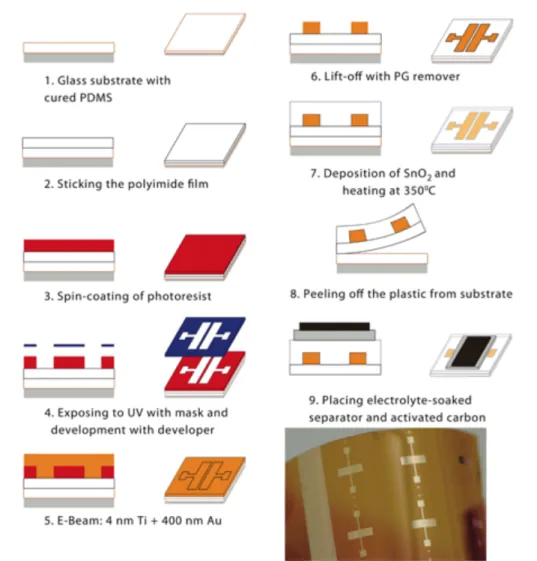
Figure 2-9: Schematic illustration of VO2 EGT devices with (a) planar gate geometry, and (b) vertical gate geometry. Reprinted with permission from [107]. Copyright 2012 AIP Publishing LLC. ... 31 Figure 3-1: Process flow for the fabrication of SnO2 EG transistors on flexible polyimide
substrates and a photo of a final device (unpatterned flexible devices indicated as D). The geometric area of SnO2 in contact with the electrolyte is 0.36 cm2, i.e. the area of the
Durapore® membrane filter soaked in the ionic liquid [EMIM][TFSI]. The thermal treatment temperature of SnO2 film was 350 °C. ... 39
Figure 3-2: Output characteristics of different types of [EMIM][TFSI]-gated SnO2 transistors
(scan rate 50 mV/s). Patterned devices on Si/SiO2:a) type A and b) type B, with Vg varying
from 1 V to -1 V with steps of 0.5V. Unpatterned SnO2 transistors on Si/SiO2 and flexible
substrates: c) type C and d) type D, at Vg =0V, 0.3V, 0.5V, 0.7V, 1V. ... 40
Figure 3-3: Transfer characteristics in the linear regime of [EMIM][TFSI]-gated SnO2 transistors
at Vd=0.2 V. Devices working in depletion mode: a) small pattern A and b) large pattern B.
Devices working in enhancement mode: c) unpatterned transistors C and unpatterned transistors D. Scan rate 50 mV/s. ... 41 Figure 3-4: Cyclic voltammetry of SnO2 films in transistor configuration for the patterned and
unpatterned devices a) A, b) B, c) C, and d) D (see main text) in the electrolyte [EMIM][TFSI], at scan rates 10, 25, 50, 100 mV/s. The current is normalized to the surface area of the SnO2 films as deduced using the results of the BET measurements for the
specific surface area. ... 44 Figure 3-5: Output characteristics of [EMIM][TFSI]-gated SnO2 transistors on polyimide, under
bending at: a) R=30 mm and b) R=10 mm. Vg = 0 V, 0.3 V, 0.5 V, 0.7 V, 1 V. Scan rate 50
mV/s. The thermal treatment temperature of SnO2 films is 350 °C. ... 45
Figure 4-1: Steps for device fabrication including patterning of TiO2 films with ParyleneC. Two
types of patterns were used: covering the transistor channel and overlapping 20 µm over each Au electrode (pattern A, TiO2 geometric area of 0.0025 cm2); covering the transistor
channel and overlapping about 500 mm over each Au electrode (pattern B, TiO2 geometric
geometric area of 0.36 cm2). [EMIM][TFSI], soaked in a membrane filter (Durapore®, 9
mm×4 mm×125 µm), is used as the electrolyte. Activated carbon (6 mm×3 mm×170 µm) acts as the gate. ... 53 Figure 4-2: Cyclic voltammetry of TiO2 films of different geometric areas and surface areas (see
main text): a) A; b) B c) C, in the electrolyte [EMIM][TFSI], at different sweeping rates (see legend). A TiO2 film included between source and drain electrodes acts as the working
electrode and the carbon gate acts as the counter and the quasi reference electrode. The current is normalized to the surface area of the TiO2 films in contact with the electrolyte. d)
Nyquist plots obtained in transistor configuration using TiO2 films of different surface areas
included between source and drain as the working electrode and carbon as the counter and quasi reference electrode; the measurements were carried out at 1 V vs carbon quasi reference electrode, using [EMIM][TFSI] as the electrolyte. ... 55 Figure 4-3: Output characteristics at Vg = 0 V, 1 V, 1.2 V, 1.3 V, 1.5 V and transfer
characteristics at Vd = 200 mV of [EMIM][TFSI]-gated TiO2 transistors: a) and b) are for
films A; c) and d) for films B; e) and f) for unpatterned films C. The sweeping rate is 50 mV/s. ... 58 Figure 5-1: Scanning electron microscopy and X ray diffraction images of (a,c) Ebeam evaporated and (b,c) solution processed TiO2 films on Si/SiO2 annealed at 450 C. ... 67
Figure 5-2: (a,d) Output characteristics at Vg = 0 V, 1 V, 1.2 V, 1.3 V, 1.5 V and (b,e) transfer
characteristics at Vd = 200 mV; (c,f) transfer characteristics at Vd = 1V of
[EMIM][TFSI]-gated TiO2 transistors: a), b), c) are for evaporated films A; d), f) and e) for solution
processed films B. The scan rate is 50 mV/s. ... 68 Figure 5-3: Cyclic voltammetry of TiO2 films for evaporated devices type A (a,c) and solution
processed type B (b,d). A TiO2 film included between source and drain electrodes, acts as
the working electrode and the carbon gate acts as the counter and the quasi reference electrode. For (c,d) the current is normalized to the surface area of the TiO2 films in contact
with the electrolyte. The measurements were carried out at scan rate 50 mV/s using [EMIM][TFSI] as the electrolyte. ... 69
Figure 5-4: Nyquist plots obtained in transistor configuration using dense (A) and porous (B) films of TiO2 included between source and drain as the working electrode and carbon as the
counter and quasi reference electrode. (b) Phase angle vs frequency of the same devices. In samples A the film has a geometric surface area of 0.4 cm2, in samples B the BET surface area is of 170 cm2. The measurements were carried out at 1 V vs carbon quasi reference electrode, using [EMIM][TFSI] as the electrolyte. ... 71 Figure 5-5: Output characteristics at Vg = 0 V, 1 V, 1.2 V, 1.3 V, 1.5 V at sweeping rate (a) 50
mV/s; (b) 50 mV/30s and (c) 50 mV/60s. (d) Transfer characteristics at Vd = 200 mV; (e)
transfer characteristics at Vd = 1V of evaporated TiO2 TFTs with [EMIM][TFSI] Lithium
perchlorate as gating medium (device C). ... 72 Figure 5-6: Output characteristics at Vg = 0 V, 1 V, 1.2 V, 1.3 V, 1.5 V at sweeping rate (a) 50
mV/s; (b) 50 mV/30s and (c) 50 mV/60s. (d) Transfer characteristics at Vd = 200 mV; (e)
transfer characteristics at Vd = 1V of porous solution processed TiO2 TFTs with
[EMIM][TFSI] Lithium perchlorate as gating medium (device D). ... 73 Figure 5-7: Cyclic voltammetry of TiO2 films for devices type C (a,c) and D (b,d). A TiO2 film
included between source and drain electrodes acts as the working electrode and the carbon gate acts as the counter and the quasi reference electrode. For (c,d) the current is normalized to the surface area of the TiO2 films in contact with the electrolyte. The measurements were
carried out at scan rate 50 mV/s using [EMIM][TFSI]+Lithium perchlorate as the electrolyte. ... 75
LIST OF SYMBOLS AND ABBREVIATIONS
a-GSZO Amorphous gallium tin zinc oxide
a-HfO2 Amorphous hafnium oxide
Ag Silver
AIZO Aluminum indium zinc oxide
Al2O3 Aluminium oxide
ALD Atomic layer deposition
Au Gold
AZO Aluminum zinc oxide
BC-BG Bottom contacts - bottom gate
BC-TG Bottom contacts - top gate
BJT Bipolar junction transistor
C Capacitance
C gate medium Cpecific capacitance of dielectric
CB Conduction band
CdS Cadmium sulphide
Cov Overlap capacitance
CV Cyclic voltammetry
[DEME]-[TFSI] N,N-diethyl- N-(2-methoxyethyl)- N -methylammoniumbis-(trifluoromethylsulfonyl)-imide
D Drain electrode
d Thickness of the insulator
[EMIM][TFSI] 1-ethyl-3-methylimidazolium
Eg Band-gap energy
EGT Electrolyte gated transistors
Ex(x) Electric field
FET Field effect transistor
ft Transit frequency
G Gate electrode
Ga Gallium
gm Transconductance
HRTEM high resolution transmission electron microscopy
Id Drain current
Idsat Saturation drain current
IGZO Gallium tin zinc oxide
Ioff Current in off state of transistor
Ion Current in on state of transistor
ITO Indium tin oxide
IZO Indium zinc oxide
k Boltzmann constant
L Channel length
Li Lithium
Loverlap Width of overlapping electrodes
MeO Metal oxide
MOCVD Metal oxide chemical vapor deposition
MOSFET Metal-oxide-semiconductor field-effect
NaOH Sodium hydroxide
Nt Total trap density
PANI Polyaniline
PBS Phosphate-buffered saline
PEDOT:PSS Poly(3,4-ethylenedioxythiophene):polystyrenesulfonate
PEN Polyethylene naphthalate
PET Polyethylene terephthalate
PI Polyimide
Pt Platinum
PVA Poly(vinyl alcohol)
q Elementary charge Q Mobile charges Rc Contact resistance S Source electrode S3N4 Trisulfur tetranitride Sb Antimony
SnO2 Tin dioxide
Ta2O5 Tantalum pentoxide
TC-BG Top contacts - bottom gate
TC-TG Top contacts - top gate
TFT Thin film transistor
Ti Titanium
TiO2 Titanium dioxide
Vd Drain voltage
Veff Effective voltage
Vg Gate voltage
Vth Threshold voltage
W Channel width
WO3 Tungsten trioxide
WO4 Orthotungstate
Woverlap Length of overlapping electrodes
Y2O3 Yttrium oxide
Zn(OAc)2 Zinc acetate
Zn(OH)2 Aqueous ammonia
Zn2+ Zinc ion
ZnO Zinc oxide
ZnO:Li Lithium - doped zinc oxide
ZnO•xH2O ZnO hydrate
ZrO2 Zirconium dioxide
ZrOx Zirconium oxide
ZTO Zinc tin oxide
ε Vacuum permittivity
εs Permittivity of semiconductor
LIST OF APPENDICES
APPENDIX A – SUPORTING INFORMATION FOR THE ARTICLE 1
... 95APPENDIX B – SUPPORTING INFORMATION FOR THE ARTICLE 2
... 109APPENDIX C – LIST OF PUBLICATIONS IN POLYTECHNIQUE MONTREAL
NOT INCLUDED IN THE THESIS
... 117CHAPTER 1 INTRODUCTION
The objectives of this chapter are to give a brief overview of transistor technology as well as the structure and the working principle of thin film transistors (TFT). In particular, I will discuss metal oxides used in this work as semiconductor materials and electrolyte gating principles.
1.1 History of transistors
The first reported transistors were based on field effect. In 1925, the Austro-Hungarian physicist Julius Edgar Lilienfeld patented the operating principles of field effect transistors (FET).[1] The first field effect transistor was patented in 1934 by the German Physicist Oscar Hale.[2] In 1959 scientists from Bell Labs manufactured a metal-oxide-semiconductor field-effect transistor (MOSFET). The first MOSFETs were commercialized in 1963.[3]
Meanwhile, in 1947, the Bell Labs scientists John Bardeen, William Shockley and Walter Brattain invented the point contact transistor, one of the type of bipolar junction transistor (BJT).[4, 5] By means of a simple device, consisting of a paper clip, a small amount of germanium and golden foil, they could amplify an input current by 100 times. In the point contact transistor the low current input terminal is emitter and amplified current output is between base and collector. In 1951 they invented bipolar junction transistor, which is used up till now. In this transistor, the input terminal is base and the amplified current is collected between emitter and collector. In 1956 they were awarded the Nobel Prize in Physics for their “researches on semiconductors and their discovery of the transistor effect”.[6] In 1954, J. Bardeen and W. H. Brattain reported that gaseous ionic species adsorbed on germanium surface causes a change in the surface dipole and hence the conductivity of the germanium, leading to the development of gas sensors.[7] In 1955, their experiment was extended by to the surface of germanium electrodes in contact with aqueous electrolytes. This experiment is often considered as the first example of electrolyte gating.[8]
Early transistors were connected as individual components to other elements like resistors, diodes, capacitors and others on the board to make a circuit. In 1958, to make these circuits boards faster, Jack Kilby proposed the idea that all circuit components can be formed on one semiconductor crystal adding only the interconnections. Later, he fabricated two transistors on
the same silicon crystal leading to the first integrated circuit. Nowadays, it is possible to fit more than a billion transistors on a single crystal. Jack Kilby was awarded the Nobel Prize in Physics for the invention of the integrated circuit in 2000.[6]
The first thin film FET was developed in the RCA laboratory by Weimer in 1961. Polycrystalline cadmium sulphide (CdS) was the material used for the semiconducting thin-film and silicon monoxide, SiO, was the insulator.[9] In 1964, the first metal oxide (MeO) TFT, using evaporated SnO2 as the semiconductor, was introduced by Klasens.[10] Later, TFTs with SnO2 deposited by
vapor phase reactions were introduced in 1970 by Aoki.[11] Single crystal lithium- doped zinc oxide (ZnO:Li) TFTs hydrothermally grown from solution had a very good electrical properties, such as hall mobility 220 cm2/Vs.[12]
With the invention of a transistor the techno-science progress was spinned with a new force. In the 1950s the first transistor radio was produced. In 1960, the first fully transistorized portable television appeared. In 1971, the first pocket calculator was fabricated. In 1983, after the invention of the mobile phone, the era of mobile communication began. Today, transistors are facing an explosive evolution towards the light weight, flexible, stretchable and biocompatible electronics for many applications, such as wearable and textile integrated systems [13-17], flexible and rollable displays [18, 19], medical implants [20] and artificial skin [21, 22] among others.
1.2 Thin film transistors
A thin film transistor (TFT) is a transistor where metal contacts and semiconductor material are deposited as thin films. The semiconductor film is separated from the gate electrode (G) by an electrically insulating dielectric. Source (S) and drain (D) electrodes, of given channel width (W) and length (L), inject charges into the semiconductor. TFTs can use several semiconductor materials, such as silicon, compound semiconductors, carbon nanotubes, metal oxides or organic semiconductors.[23-29]
The working principles of TFTs, their characteristics and components will be described below. All transistors components have an influence on the transistor characteristics and should be optimized for different applications.
1.2.1 Working principle of thin film transistors
Figure 1.1 represents the working mechanism of a thin film field effect transistor. A gate electrode, insulator and semiconductor form a capacitor. By applying, for example, a positive voltage, Vg, to the gate, while the source electrode is grounded, negative charge carriers start to
accumulate in the channel. When the gate-source voltage exceeds the threshold voltage (Vg > Vth)
the channel becomes conductive.
If a voltage is applied between the drain and the source (Vd), a current starts to flow between the
two electrodes (drain-source current, Id). By gradually increasing Vd, the source-drain current
increases till reaching a saturation point, this region is called a linear region due to linear increase of current. When Vd exceeds the effective gate voltage, Veff (Vd > Vg - Vth), the gate potential
gets compensated by the drain potential and the channel is pinched off at the drain. This means that the transistor reaches the saturation regime, where further increase in Vd does not affect Idsat.
Further increase of the Vd will only move the pinch off point closer to the source, thus shortening
the channel length. The current will still be flowing from the drain to the source but will not increase, since the depletion region near the drain is lacking the majority charge carriers. The current will be sustained by the carriers injected directly from the electrode. The current flowing in the depletion region is called space-charge limited current and depends only on mobility and not on the charge carrier density. The gate voltage should regulate the distribution of charges within the channel. In the case of short channel devices, the drain field becomes stronger than the gate potential and the gate can not control the current in the transistor. Thus, the space-charge limited current will prevent saturation. So the channel length of transistor should be several times the thickness of dielectric.[30]
Figure 1-1: Schematic illustration of operating regimes of field effect transistors: (a) linear regime; (b) saturation regime at pinch-off; (c) corresponding current voltage characteristics. The specific capacitance of the gate insulator is given by the formula :
𝐶 =!!"! , where ε is the vacuum permittivity, k is the relative permittivity (dielectric constant), A
is the area and d is the thickness of the insulator.
Therefore, the mobile charge density can be calculated from the following formula: 𝑄 = 𝐶 𝑉! − 𝑉! .
This charge density is given when Vd = 0. As soon as the drain voltage increases, the charge
density will be a function of the distance from the source. The potential will gradually increase from the source to the drain and the charge density can be given as follows:
𝑄 𝑥 = 𝐶 𝑉!− 𝑉!− 𝑉 𝑥 .
We can then derive the general formula for the drain current:
Substituting 𝐸! 𝑥 =!" !
!" and Q(x) into this formula and integrating over x we get the
following relationship: 𝐼! = !!!! 𝑉!− 𝑉! 𝑉! −!!
!
! .
Knowing that in the linear mode Vd << Vg-Vt and in the saturation mode Vd = Vg-Vt the above
equation can be simplified to the following: Linear: 𝐼! =!!!! 𝑉! − 𝑉! 𝑉!,
Saturation: 𝐼! =!!!!! 𝑉! − 𝑉! !.
1.2.2 Main characteristics of thin film transistors
The charge carrier mobility describes the efficiency of the charge carrier transport, i.e. how fast carriers can travel through the semiconductor. This parameter can be derived from Id in the linear
and saturation regimes. The charge carrier mobility values in saturation regime tell us about the efficiency of charge carrier transport when channel is formed, while in linear regime channel can be still in formation process. If contacts are ohmic the charge carrier mobility in linear and saturation regimes should be quite similar due to the same amount of charges in both regimes. Linear : µ!"# = !"!! ! !"! !!! . Saturation : µ!"# =!"!! ! !!!!"#$ ! ! .
The charge carrier mobility in TFT configuration is usually different from intrinsic mobility, which is typically determined by the Hall effect in the bulk material. Charge transport in TFTs occurs in a narrow channel region close to the gate dielectric/semiconductor interface, where different sources of scattering are taking place, such as Coulomb scattering from dielectric charges, surface roughness scattering and others.[31]
The channel current on/off ratio (Ion/Ioff ratio) is the ratio between the channel current in the on
state and the current in the off state of the transistor, which is typically extracted from the transfer curves. The off current increases the static power consumption, so minimizing it is important.
Transistors can operate in enhancement (accumulation) or depletion mode. In absence of an applied Vg, enhancement mode transistors are in the off state (Id ≈ 0), while depletion mode
transistors are in the on state (Id ≠ 0) and application of a Vg is needed to turn them off.
Enhancement mode transistors decrease the free-running power consumption and are thus preferred for applications in circuits and display technology.
Another important parameter of TFTs is the threshold voltage (Vth), i.e. the minimum gate
voltage required for a drain source current to flow when the transistor channel is formed. The Vth
depends on the semiconductor material as well as the type of dielectric, their interface, defect states, impurities and device geometry. [Veres, 2004] The most common methods to determine Vth is linear extrapolation from Id versus Vg curves at low Vd (transfer curves in liner regime) or
linear extrapolation from 𝐼! vs Vg curves at high Vd (transfer curves in saturation regime).
When a n type transistor operates in the enhancement mode, Vth is positive, and negative in
depletion mode of operation. Increasing the gate capacitance can reduce the threshold voltage. At higher capacitance more charges are induced in the channel making it conductive at lower voltages.
The transconductance, gm, describes how the drain current is modulated by the gate voltage, and
it is defined as:
𝑔! = !!!
!!! ! !
The transconductance describes the behavior of the transistor at gate voltages above the threshold when the current originates from the drift of charges from source to drain. In the subthreshold regime (Vg < Vth), the current is mostly originated by diffusion of charges. In this regime the
important parameter is subthreshold swing.
The value of subthreshold swing is extracted from the plot of the logarithm of the drain current versus the gate voltage at a constant drain voltage (linear or subthreshold regime). It measures the amount of Vg change required to increase Id by an order of magnitude in the subthreshold region.
The subthreshold swing is represented by the following equation: 𝑆 = !!!
The knowledge of subthreshold swing can give information about the total defect density at the semiconductor dielectric interface.[32] The total trap density, Nt, can be found from the equation:
𝑁! = ! !"#(!)!" ! − 1 𝐶 !!!!!, where, k is the Boltzmann constant, q is the elementary charge, 𝜀! is the permittivity of the semiconductor and C the dielectric capacitance.[33]
1.2.3 Thin film transistor configurations
Transistor performance significantly depends on the device configuration. The four main transistor configurations are presented in Figure 1.2.
Figure 1-2: Schematic illustration of thin film transistor configurations: bottom contacts - bottom gate (a, BC-BG), bottom contacts - top gate (b, BC-TG), top contacts - bottom gate (c, TC-BG)
and top contacts - top gate (d, TC-TG).
In these device configurations, the injected charges travel different distances to reach the semiconductor/dielectric interface, i.e. the region where charge transport takes place. For instance, in the BC-BG and TC-TG configurations charges are injected directly close to the semiconductor/dielectric, whereas, in the BC-TG and TC-BG structures the injected charges must travel through the whole thickness of the semiconductor to reach the channel. Thus, the device configuration can affect the main figures of merit of the transistor, such as the threshold voltage and the charge carrier mobility. For instance, a large surface of the source and drain electrodes
overlapping the gate electrode can result in improved charge injection, leading to a small contact resistance.[34]
1.2.4 The contact resistance and overlap capacitance
Charge exchange (injection and extraction) depends on the workfunction of electrode and the bandgap of the semiconductor. When the workfunction of the electrode is close to the conduction or valence bands of the semiconductor the charges are easily injected and the contacts are called ohmic. A mismatch between the workfunction and the conduction band is called an injection barrier (Schottky barrier). This introduces a resistance to the transistor (contact resistance, Rc). The contact resistance can be significantly larger than the channel resistance depending on the channel length, applied voltage and mobility of the carriers. So, it is especially important to control Rc in short channel devices (L ≤ 5um) as it dominates over the total resistance and leads to degradation of electrical properties.[33]
The contacts materials in transistors are high work function metals such as Au, Ag, Pt. Conducting polymers, such as PEDOT:PSS, PANI [35-37], graphene and carbon nanotubes, can also be used.[38, 39] The high aspect ratio and 1D structure of carbon nanotubes facilitates charge carrier injection by tunneling and their low density of states provides a lever to further reduce the Schottky barrier height and width.
The overlap capacitance (Cov) is the capacitance between the overlapping parts of source-drain
contacts with the gate and it doesn’t depend on the applied potential. It can be found by the formula:
𝐶!" = (LW)overlapCgate medium , where L,Woverlap is the length and width of overlapping electrodes
and C gate medium is the specific capacitance of dielectric.
The total capacitance of the transistor is:
𝐶!"!#$ = 𝐶!!!""#$+ 𝐶!", where Cchannel is a capacitance between gate electrode and channel
responsible for transistor operation.[40]
In the case of high-k dielectric materials or electrolytes as a gating media, the total capacitance is high enough that the overlap capacitance becomes negligible. The overlap capacitance directly
influences the transit frequency of transistors, (ft), which quantifies the speed of the device.[41]
1.3 Electrolyte gated thin film transistors
A high operating voltage (tens of volts) is typically needed in conventional TFTs, due to the low capacitance. Typical dielectric materials, such as SiO2 (k~3.9) or S3N4 (k~7) or others, possess
capacitance density in the range of 0.005~0.5 µF cm-2, depending on the thickness and dielectric
constant.[42-44] Reducing the thickness of conventional dielectrics to achieve high capacitance can lead to high leakage current and reliability issues. The use of high-k dielectric materials such as ZrO2 (k~20), Ta2O5 (~25), or TiO2 (~40) can increase the capacitance without significant gate
current leakage.[45]
Another way to achieve a high capacitance and charge carrier density modulation is electrolyte- gating [46-49], where the gate dielectric is replaced by an electrolyte. By applying a gate voltage, the electrolyte ions redistribute at the electrolyte/semiconductor interface, forming a thin electrical double layer (EDL). The small thickness of the double layer (~1nm) formed on the electrolyte semiconductor interface leads to high capacitance (typically 1-10 µF/c2),which allows the transistor to operate at low voltages (less than 2 V).[50, 51]
The mode of operation of electrolyte-gated transistors is mainly governed by one or the two doping processes described below: electrostatic and/or electrochemical.[52, 53] For semiconductors, which are impermeable to ions, the double layer forming at interface with the electrolyte results in a gating mechanism similar to that taking place in field effect transistors (electrostatic, as shown on Figure 1.3a). For semiconductors which are permeable to ions, upon application of gate voltage, ions can have reversible redox reactions on the surface (electrosorption) or ions can enter the film leading to reversible redox reactions (intercalation), thus changing the charge carrier density and hence the conductivity of the film (as shown on Figure 1.3b).[54] It is worth noting that, in real devices, electrostatic and electrochemical doping may occur at the same time.[49, 55]. This faradaic charge transfer is called pseudocapacitance.
Figure 1-3:Schematic illustration of an electrolyte gated thin film transistors operating in field effect (a) and electrochemical mode (b).
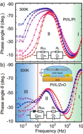
The gate electrode, electrolyte and semiconductor as a second electrode form a capacitor. The electrolytic capacitance depends on the applied potential and frequency. It can be examined by impedance spectroscopy or cyclic voltammetry.[46, 56, 57] The equivalent circuit for such capacitor structure can be modeled as two resistor-capacitor (RC) circuits in series, see figure 1.4. One RC is related to the bulk of electrolyte and another one is related to the double layer.[58] [Yuan, 2010] Each RC circuit has a specific frequency domain and can be identified from the Bode plot (phase angle vs. frequency). At high frequencies (above 100 kHz) there is a bulk capacitive region (polarization of the bulk electrolyte); for the frequency range (10kHz to 1Hz) there is a EDL capacitive region, and below 1 Hz there is a EDL pseudocapasitive region (related to chemical processes on the electrolyte/semiconductor interfaces).
The total capacitor impedance (Z) is the sum of the real part (Z′) and imaginary part (Z′′): Z = Z′ + iZ′′, where i is the imaginary unit.
When the electrolyte exhibits capacitive behavior at low frequency and resistive behavior at high frequency, the total impedance depends on the ohmic resistance R and on the electric double layer capacitance CEDL:
Z = R + i2πf CEDL, where f is the frequency and CEDL is the capacitance of the electric double
layer.
The imaginary part of the impedance is inversely proportional to the capacitance, thus C = 1/(2πfZ′′).
The capacitance can also be calculated from cyclic voltammetry, where the integration of b)
voltametric current over time provides the amount of doping charges Q. And, capacitance can be deduced from the slope of the (linear) plot of the doping charge vs. potential: C= Q/V.
Figure 1-4: Example of the Bode plot (θ-f) in Pt/IL/Pt structure. Inset: equivalent electric circuit, two resistor-capacitor (RC) circuits in series. (b) The Bode plot of ZnO EDL transistor. I: bulk IL
capacitive region. II: electrostatic EDL capacitive region; III: electrochemical pseudocapacitive region. Reprinted with permission from [58]. Copyright 2010 American Chemical Society.
1.4 Metal oxides (TiO
2and SnO
2) as semiconductors
Metal oxides (MeO) are among the most popular channel materials in transistors, especially in next generation flexible and transparent transistors, due to their superior electrical properties and high reliability.[46, 59] The more utilized metal oxides in optoelectronic applications are transition and post transition metal oxides. The transition metals exhibit multiple oxidation states. Their compounds in higher oxidation states are strong oxidizing agents, as they tend to accept electrons to reach a stable lower oxidation state.
Electronic structures and charge transport mechanisms of metal oxides are quite different from conventional covalent semiconductors like silicon. CB of silicon formed by sp3 σ-bonding and VB by sp3 σ*-antibonding, and the band gap is the energy difference between them. In this case, any structural change will influence the charge transport decreasing the charge mobility. For instance, at a carrier density of 1019 cm3 the electron mobility in a single crystalline and amorphous silicon is around 200 cm2/Vs and 1 cm2/Vs, respectively.[60] In metal oxides the band structure is different. The conduction path in crystalline and amorphous covalent semiconductors and post transition MeOs is shown in Figure 1.5.
Figure 1-5: Schematic illustration of orbitals for the carrier transport paths in crystalline and amorphous covalent semiconductors and post transition MeOs. a) the band structure in covalent semiconductors, like silicon, consists of overlapping sp3 orbitals, so structural randomness greatly
degrades the magnitude of bond overlap. b) In post transition oxide semiconductors, spheres represent metal s orbitals (conduction band), the contribution of 2p orbitals (valence band) is small. The spread of metal s orbitals is high and their overlap doesn’t significantly affected in
amorphous state. Reprinted with permission from[60] © Nature Publishing Group, 2004. In most metal oxide semiconductors, due to the high electronegativity of O, there are covalent bonds with a strong degree of ionicity. The ionicity creates an electronic structure where 2p orbitals of O form the valence band (VB) and the highest occupied metal orbitals form the conduction band (CB). In the case of transition metals, the conduction band consists of localized d orbitals. In the case of post transition metals, the conduction band consists of delocalized ns (n ≥ 4) orbitals.[60, 61] The overlap of big s orbitals is insensitive to distorted metal-oxygen-metal bonds in amorphous state.[62] Thus, the charge carrier mobilities of amorphous post transition MeOs can be similar to ones of crystalline.
In this work, I studied the main representatives of binary transition and post transition metal oxides TiO2 and SnO2, respectively. They possess similar crystal structures (Figure 1.6) and
chemical bonds, and are comparable in electronic band-gap energies (Eg ≈ 3–4 eV). However, the electronic properties are quite different. The TiO2 has weak electron conductivity and optical
absorption to UV light. While SnO2 combine electrical conductivity and optical transparency to
Figure 1-6:The crystalline structures and Brillouin zones of rutile 𝐷!"!" and anatase 𝐷
!"!". Reprinted
with permission from [61]. © AIP Publishing LLC, 2013.
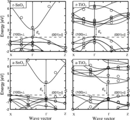
These differences can be described by their band structure. The VB formed by 2p orbitals of O are the same for all MeOs. The difference of CB, formed by Me cations, with electron configurations 5s25p2 for Sn and 3d24s2 for Ti gives rise to a single high dispersive CB for SnO
2
and to the several flat dispersed CBs for TiO2, see Figure 1.7. The overlap of high spread 5s
orbitals is responsible for the delocalization of electrons in SnO2 making the conduction band
dispersive and responsible for higher conductivity. While in TiO2, the electrons are strongly
localized in 3d orbitals making the CB flat dispersive. [60, 61]
Figure 1-7:Electronic structures of r- SnO2, r- TiO2, a- SnO2, and a- TiO2 along two main
symmetry directions (100) _|_ and (001) ||. Reprinted with permission from [61]. © AIP Publishing LLC, 2013.
1.5 Problem identification
The electrical characteristics of electrolyte-gated transistors depend on the device structure, the effective potential of gate electrode and the doping level of the semiconductor channel.
Understanding the electrical transport mechanisms in electrolyte-gated transistors is an ongoing challenge to design devices with better electronic performance. Moreover, the role played by the extension of the electrolyte/semiconductor and electrode/semiconductor interfaces on the doping and charge carrier transport processes requires deeper investigation. The overlap between the metal electrodes and the semiconductor, which is in contact with the electrolyte, might affect the charge injection process. Another challenge in the fabrication of high performance TFTs for flexible electronics, is the required low processing temperature (150 ºC in the case of polyethylene naphthalate (PEN) substrates, maximum 350 ºC for polyimide (PI) substrates).
1.6 General Objectives
The general objective of this Ph.D. thesis is the design, fabrication, and characterization of metal oxide electrolyte gated transistors based on TiO2 and SnO2.
The objective was accomplished by tuning the structure and the morphology of semiconductor materials (SnO2 and TiO2) as well as by selecting the appropriate gating media. To control the
charge carrier density and understand the doping mechanism in the electrolyte gated TFT, patterning of the semiconductor material with different overlap of source-drain electrodes was implemented. SnO2 TFTs were also fabricated on PI substrate and their electrical and mechanical
properties were investigated to show high performance TFT for applications in flexible electronics.
1.7 Motivation
Environmentally friendly and abundant metal oxides as SnO2 and TiO2 are promising transistors
channels for flexible displays, medical implants and sensors, wearable electronics etc. Electrolyte gating allows TFTs to work at low voltages, which is critical for bio applications. Fabrication of high performance electrolyte gated TFTs and shedding light on their electrical, electrochemical and mechanical properties make an invaluable contribution to bio and flexible electronics.
1.8 Specific objectives
To achieve the main objective the following specific objectives need to be achieved:
1. Charge carrier density modulation of metal oxide thin films for electrolyte gated
By electrostatic and/or electrochemical doping, it is possible to exhibit a transition from insulator to semiconductor or metal like behavior. A high charge carrier density was achieved in TiO2 and
SnO2 films by electrolyte gating. The fabrication of devices with different surface areas of
semiconductor material in contact with the electrolyte and different overlaps with source-drain electrodes helped to tune the electrical properties of devices, to shed light on the charge transport mechanisms and to explore the best device geometry for high performance devices. The doping mechanisms were investigated by Electrical characterization, cyclic voltammetry (CV) and Electrical impedance spectroscopy.
2. Fabrication of high performance flexible electrolyte gated transistors
To make metal oxide thin films with good structural and electrical properties, high temperature annealing is needed. So the development of deposition of metal oxide thin films at temperatures of 350◦C or lower is required for application in flexible electronics. Electrical and electrochemical characterization of flexible transistors were conducted. Moreover, to show the mechanical stability, electrical characterization of transistors was accomplished after repeating mechanical deformations.
3. Tuning of the structure and morphology of transistor semiconductors and exploring the effect of ion size in electrolytes on transistors performance
To explore the effect of structure and morphology of semiconductors on transistor performance, porous solution processed and highly dense evaporated films of TiO2 were investigated. The
relatively large [EMIM] cation cannot enter into the crystal lattice of TiO2. It was shown that
only small cations such as Li+ can be intercalated through the “zig- zag” rows formed at edge-shared octahedral of the tetragonal form of anatase TiO2. The effect of big [EMIM] and small Li+
cations on doping mechanisms was introduced.
1.9 Organization of the work
This thesis is organized into the seven Chapters. Chapter 1 includes an overview of the topics related to the subject of the thesis (thin film transistors, their working principles and characteristics, electrolyte gated transistors and an introduction of metal oxides used in this thesis: TiO2 and SnO2), problem identification and objectives of the thesis. Chapter 2 introduces
the state of the art of thin film transistors, in particular metal oxide electrolyte gated transistors. Chapters 3, 4 correspond to two articles of which I was the first author.
Article 1: Tin dioxide electrolyte-gated transistors working in depletion and enhancement mode. (Submitted in ACS Appl. Mater. Interfaces).
Article 2: Photolithographically Patterned TiO2 Films for Electrolyte-Gated Transistors
(Published in ACS Appl. Mater. Interfaces, 8, 14855−14862, 2016).
Chapter 5 is devoted to investigation of effect of different morphology of TiO2 and cations size in
the electrolyte on doping mechanisms of TiO2 electrolyte gated transistors. (It is a third paper in
preparation where I am the first author and it will be submitted soon.) Chapter 6 is about “General Discussion”.
Chapter 7 contains the conclusions and perspectives on the future work.
Appendix A and B contain all supporting information of articles 1 and 2, respectively. Appendix C is a list of articles, published during this Ph. D., not included into this thesis. Appendix D is a list of conferences in which I took part.
CHAPTER 2 LITERATURE REVIEW: METAL OXIDE THIN FILM
TRANSISTORS
Metal oxides are attracting enormous interest for TFT technology, due to their electrical, optical and chemical properties.[64, 65] Most of them have a wide band gap, good stability and high charge carrier mobility; they are optically transparent in visible light, making them attractive for transparent TFTs in flat panel displays.[27, 66] Moreover, a lot of metal oxides possess bio-compatible and non-toxic properties making them attractive for bio electronics, such as variety of biosensors.[67] Some oxides have good electrical properties in amorphous state making them the materials of choice for flexible and bendable electronics.[41, 68, 69]
2.1 Vapor processed thin film transistors
The main binary oxides used in TFTs are ZnO, SnO2 and In2O3 due to their good electrical
properties, high transparency and biocompatibility. The review of SnO2 TFTs will be covered in
the following paper. ZnO TFTs deposited by radiofrequency magnetron sputtering at room temperature were introduced by Carcia.[70] The influence of different oxygen partial pressure during vacuum deposition on the stoichiometry of the metal oxide film was shown. The highest electron mobility was 40 cm2V-1s-1 and on/off ratio 103 for TFTs where ZnO films were deposited at oxygen partial pressure 10-6 Torr. The highest on/off ratio 106 with electron mobility 1.6 cm2V-1s-1 was achieved for device fabricated at oxygen partial pressure 10-5 Torr due to the fewer amounts of oxygen vacancies and so lower conductivity and off current. A depletion mode ZnO transistors with an electron mobility of 23.3 cm2V-1s-1 were demonstrated by Mi. [71] ZnO was deposited by metal oxide chemical vapor deposition and the Al2O3 dielectric was deposited
by Atomic Layer Deposition (ALD). An on-off ratio of 106 and a threshold voltage of -4.8 V were achieved. Lin et al. demonstrated flexible ZnO TFTs where both the dielectric and the semiconductor films were deposited by ALD at 110 °C (Figure 2.1). ALD permits the deposition of defect-free films with minimal defects in the interface at low temperature. The electron mobility was 16.6 cm2/V·s and was increased up to 20 cm2/V·s after passivation of the ZnO layer
by TiO2(3 nm)/Al2O3(2 nm) nanolaminate. The passivation layer not only improved the electrical
Figure 2-1: (a) Schematic illustration of ZnO transistor; (b) transfer and (c) output characteristics of this transistor without passivation layer. Reprinted with permission from [73]. Copyright ©
2015 American Chemical Society
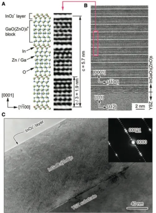
Hosono and colleagues started a new era of ternary and quaternary MeO by synthesizing indium gallium zinc oxide (IGZO) grown by reactive solid-phase epitaxy at room temperature.[74] An electron mobility of 80 cm2V-1s-1 and an on/off ratio of 106 was achieved by making use of a-high k HfO2 dielectric (with dielectric constant 18) and mobility 2 cm2V-1s-1 was achieved using an
amorphous aluminum oxide dielectric. Making use of high k dielectric significantly increases the capacitance and charge carrier density in the IGZO leading to high mobility. The layered lattice structure compose of InO!! and GaO(ZnO)
!
! stacked along the (001) direction was shown by high
resolution transmission electron microscopy (HRTEM), see figure 2.2. It is worth to notice that Ga3+ replacing Zn2+ in tetrahedral sites maintained the electroneutrality. Moreover, Ga ions formed stronger chemical bonds with oxygen thus suppressing the oxygen vacancy formation. InO2 worked as a passivation layer, preventing O2 out-diffusion. Later, the same group published
electrodes and Y2O3 dielectric, where IGZO was also deposited by pulsed laser deposition. An
electron mobility of 7 cm2V-1s-1 and an on/off of 103 were measured also under bending.[60]
Figure 2-2: Structure of InGaO3(ZnO)5. (A) Schematic illustration of the crystal structure. A
HRTEM lattice image is shown for comparison. (B,C) Cross-sectional HRTEM images of a InGaO3(ZnO)5 thin film grown by reactive solid-phase epitaxy. Reprinted with permission from
[74]. Copyright 2003 The American Association for the Advancement of Science
electronic configuration like zinc tin oxide (ZTO) [75], indium zinc oxide (IZO) [59, 76, 77], IGZO [60], aluminium zinc oxide (AZO).[78] Multi components compounds easily formed amorphous films, due to the different ionic charges and sizes of each component. Amorphous MeOs attract more and more attention because of their low processing temperatures and a more uniform surface, leading to better electrical characteristics.[79]
Amorphous zinc tin oxide TFTs with good electrical properties (on/off of 107, field effect mobility around 5-15 cm2V-1s-1) were introduced by Chiang and others. The zinc tin oxide was deposited by radiofrequency magnetron sputtering. After a high temperature treatment at 600 ºC the mobility values were increased up to 20-50 cm2V-1s-1 and the on/off was higher than 107.[75] Amorphous gallium tin zinc oxide (a-GSZO) TFT films were deposited by radiofrequency magnetron co-sputtering using gallium zinc oxide and tin targets at room temperature and at 150 ºC.[80] TFT deposited at higher temperature possess better electrical performances. Higher electron mobility and higher on/off ratio (32 cm2V-1s-1 and 1010) were achieved in indium tin zinc oxide (ITZO) flexible TFTs in comparison with IGZO flexible TFTs (10 cm2V-1s-1 and 108).[81]
Inverted-staggered bottom-gate TFTs were fabricated on a polyimide film with conventional SiO2 dielectric. Moreover, 8-inch organic light emitting display (OLED) was fabricated using
(ITZO) flexible TFTs, which hindered color video even during the bent.
2.2 Solution processed thin film transistors
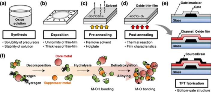
Solution processing of metal oxides, such as printing, spin coating and spray pyrolysis opens doors for large area electronics, flexible and printed electronics in ambient condition.[65] Figure 2.3 represents an example of general solution processing for many MeO deposition.[82] The first step is the synthesis of oxide solution by mixing a metal precursor and a solvent. The second step is a pre-annealing to remove the solvent. The third step is an annealing at higher temperature to form the metal oxide layer, which consists of decomposition, hydrolysis, dehydroxilation and crystallization. Hydrolysis is when the metal precursor mixed with solvent; the main intermediate products of this reaction will be radicals of metal hydroxide and other complexes. Then when the annealing temperature is high enough the thermal decomposition of metal hydroxide produce the metal oxide and liberate the water. Different annealing temperatures are needed for different oxides.

![Figure 2-4: Thermogravimetric analysis of different IZO precursors. Reprinted with permission from [82]](https://thumb-eu.123doks.com/thumbv2/123doknet/2350839.36224/46.918.250.671.106.425/figure-thermogravimetric-analysis-different-izo-precursors-reprinted-permission.webp)
![Figure 2-5: a) Schematic illustration and optical image of a van der Pauw ion‐gel‐ ([EMI][TFSI]+PS‐PMMA‐PS)‐gated printed In 2 O 3 TFT; b) Electron density from Hall effect](https://thumb-eu.123doks.com/thumbv2/123doknet/2350839.36224/50.918.112.809.194.379/figure-schematic-illustration-optical-printed-electron-density-effect.webp)