UNIVERSITÉ DE MONTRÉAL
PIXEL AND READOUT CIRCUIT OF A WIDE DYNAMIC RANGE
LINEAR-LOGARITHMIC CURRENT-MODE IMAGE SENSOR
ELHAM KHAMSEHASHARI
DÉPARTEMENT DE GÉNIE ÉLECTRIQUE, ÉCOLE POLYTECHNIQUE DE MONTRÉAL
MÉMOIRE PRÉSENTÉ EN VUE DE L‟OBTENTION DU DIPLÔME DE MAÎTRISE ÈS SCIENCES APPLIQUÉES
(GÉNIE ÉLECTRIQUE) Août 2011
UNIVERSITÉ DE MONTRÉAL
ÉCOLE POLYTECHNIQUE DE MONTRÉAL
Ce mémoire intitulé:
PIXEL AND READOUT CIRCUIT OF A WIDE DYNAMIC RANGE
LINEAR-LOGARITHMIC CURRENT-MODE IMAGE SENSOR
Présenté par : KHAMSEHASHARI Elham
en vue de l‟obtention du diplôme de : Maîtrise ès Sciences Appliquées a été dûment accepté par le jury d‟examen constitué de :
M. SAWAN Mohamad, Ph.D., président
M. AUDET Yves, Ph.D., membre et directeur de recherche
M. FAYOMI Christian, Ph.D., membre et codirecteur de recherche M. CHEBLI Robert, Ph.D., membre
DEDICATION
ACKNOWLEDGMENTS
I am grateful to many people who supported and encouraged me during the work leading to this thesis: professors, friends, and family.
I would like to express my sincere gratitude to my supervisor, Professor Yves Audet. He has been an excellent mentor and a constant source of knowledge, motivation, and encouragement throughout my graduate studies. I am also grateful to him for his financial support and to the other members of my committee for their constructive comments and precious time in serving on my supervision committee. I would like to extend my thanks to Dr. Christian Fayomi, my co-supervisor, for his guidance throughout of this research work.
My gratitude goes out to my former colleagues at Microelectronics Research Group who were always there for me with countless help and constructive discussions.
Special thanks go to my husband and my parents, who have given me unconditional love, patience, support and encouragement during this work.
Finally, I would like to thank all the staff members at the department of Electrical Engineering, especially, Laurent Mouden for his help during the laboratory testing of my prototype chip, Rejean Lepage and Jacques Girardin for their technical assistance.
RESUME
Le capteur d‟images est la partie principale de tout système d‟acquisition d‟images, quelle que soit son application. Jusqu‟à la fin des années 1990, les capteurs de type CCD ont dominé le marché en raison de leur qualité d‟image exceptionnelle. À l‟opposé des capteurs CCD, les capteurs CMOS offrent des possibilités intéressantes d‟intégrer les circuits de traitement de signal sur un même substrat en vue d‟obtenir une caméra sur puce. Entant que ces capteurs opèrent avec des tensions d‟alimentations plus faibles que celles requise par les capteurs CCD, elles possèdent une faible consommation de puissance. De plus, les coûts associés à la fabrication des capteurs CMOS sont plus faibles que ceux engendrés par les capteurs CCD. Ces caractéristiques font en sorte que les capteurs d‟images CMOS se prêtent à un plus grand nombre d‟application que leurs équivalents CCD.
Dans ce projet, l‟objectif principal est de concevoir un capteur d‟images ayant une plage dynamique élevée. Il possède l‟avantage de deux modes d‟opération, linéaire et logarithmique, ainsi qu‟une lecture en mode courant afin d‟augmenter sa plage dynamique. Les tensions d‟alimentation des technologies CMOS diminue de plus en plus, et de ce fait la plage dynamique du pixel. En fonctionnant en mode courant, on arrive à atténuer cet effet. Le projet consiste à concevoir des circuits : convoyeur de courant, „delta-reset-sampling‟ et un comparateur de courant qui sont efficaces pour les modes d‟opération linéaire et logarithmique du pixel et permettent de détecter dans quels des deux modes se situe le pixel de façon à réaliser, à l‟étage subséquent, une conversion analogique-numérique adéquate. Le pixel à trois transistors fonctionnant en mode courant utilise un transistor PMOS dans la région linéaire pour la lecture et un transistor PMOS de reset qui permet une réponse linéaire-logarithmique combinée. L'une des contributions à la non-linéarité de la réponse provient de l'effet provoqué par la résistance „on‟ du transistor „select‟. Pour éliminer cet effet, nous appliquons une fonction de linéarisation qui est effectuée dans le domaine numérique. Le mode d‟opération du pixel est déterminé dans le circuit de lecture de colonne et un signal est envoyé à l'unité de traitement numérique comme indicateur de mode.
Un prototype a été conçu et fabriqué en CMOS 0.35µm standard, 3.3V. Les résultats expérimentaux sont concluants et montrent une plage dynamique intrascènede 100 dB.
ABSTRACT
Digital cameras are rapidly becoming a dominant image capture devices. They are enabling many new applications. Charge-coupled devices (CCDs) have been the basis for solid state imaging since the 1970s. However, during the last decade, interest in CMOS imagers has increased significantly since they are capable of offering System-on-Chip (SoC) functionality. This can greatly reduce camera cost, power consumption, and size. Furthermore, by integrating innovative circuits on the same chip, the performance of CMOS image sensors could be extended beyond the capabilities of CCDs. Dynamic range is an important performance criterion for all image sensors.
This thesis presents a current-mode CMOS image sensor operating in linear-logarithmic response. The objective of this design is to improve the dynamic range of the image sensor, and to provide a method for mode detection of the image sensor response. One of the motivations of using current-mode has been the shrinking feature size of CMOS devices. This leads to the reduction of supply voltage which causes the degradation of circuit performance in term of dynamic range. Such problem can be alleviated by operating in current-mode. The column readout circuits are designed in current-mode in order to be compatible with the image sensor. The readout circuit is composed of a first-generation current conveyor, an improved current memory is employed as a delta reset sampling unit, a differential amplifier as an integrator and a dynamic comparator. The current-mode three-transistor active pixel sensor uses a PMOS readout transistor in the linear region of operation and a PMOS reset transistor that allows for a linear-logarithmic response. One of the non-linearity contributions is the effect caused by the „on‟ resistance of the select transistor. To eliminate this effect, we apply a linearization function that can be performed in the digital domain. The pixel response operation is determined in the column readout circuit and a signal is sent to the digital processing unit as an indicator. These circuits were implemented using a standard CMOS technology with no process modification. A prototype has been designed and fabricated in a standard AMS 2P4M, 3.3V, CMOS 0.35μm process from Austrian Microsystem. The experimental results
demonstrate the functionality of the circuits and a intrascene dynamic range of more than 100 dB.
TABLE OF CONTENTS
DEDICATION ... iii ACKNOWLEDGMENTS ... iv RESUME ... v ABSTRACT ... vii TABLE OF CONTENTS ... ixLIST OF FIGURES ... xii
LIST OF TABLES ... xiv
ABREVIATIONS ... xv
INTRODUCTION... 1
Motivation ... 2
Objective ... 3
CHAPTER 1 ... 4
IMAGE SENSOR ARCHITECTURE ... 4
1.1 Basic Structure of the CMOS Image Sensors and Pixels ... 4
1.2 Fill Factor ... 7
1.3 Image Sensor Characteristics and Performance ... 7
1.3.1 Dark Current ... 7
1.3.3 Dynamic Range ... 8
1.4 Linear Active Pixel Sensor ... 10
1.5 Logarithmic Active Pixel Sensor ... 11
1.6 Image Sensor with Combined Linear-Logarithmic Response ... 13
1.7 Current-Mode Response Image Sensor ... 14
1.8 Conclusion ... 15
CHAPTER 2 ... 17
DESIGN OF IMAGE SENSOR AND READOUT CIRCUIT ... 17
2.1 Introduction and Design ... 17
2.2 Pixel Architecture and Operation... 19
2.2.1 Pixel Non-linearities Analysis ... 22
2.2.2 Analytical Solution ... 24
2.3 Current-Mode Column Readout Circuits ... 27
2.3.1 Current Conveyor ... 27
2.3.2 Current-Mode Offset Cancellation Circuit ... 30
2.4 Mode Indicator Circuits ... 32
2.4.1 Integrator ... 32
2.4.2 Comparator ... 38
2.5 Conclusion ... 41
EXPERIMENTAL RESULTS ... 42
3.1 Test Requirements ... 43
3.2 Pixel Results... 44
3.2.1 Pixel Output Measurements without DRS ... 45
3.2.2 Dark Current Measurement ... 48
3.3 Performance of the DRS Circuit ... 51
3.3.1 Pixel Output Measurements with DRS ... 54
3.4 The Mode Indicator Column Circuits ... 58
3.4.1 Integrator ... 58
3.4.2 Dynamic Comparator ... 59
3.5 Results Comparison ... 61
3.6 Conclusion ... 61
CONCLUSION AND FUTURE WORK ... 63
REFERENCES ... 66
LIST OF FIGURES
Figure 1. 1 General structure of a CMOS image sensor ... 4
Figure 1. 2 Passive pixel ... 5
Figure 1. 3 Voltage mode N-type active pixel architecture ... 6
Figure 1. 4 Basic logarithmic pixel architecture ... 11
Figure 1. 5 Schematic of a linear-logarithmic pixel ... 14
Figure 1. 6 Current-mode image sensor ... 15
Figure 2. 1 Current-mode imaging system architecture ... 18
Figure 2. 2 Proposed pixel architecture ... 19
Figure 2. 3 Simulated linear current response for different width of M3p ... 23
Figure 2. 4 Simulated photodiode voltage variations as a function of time ... 24
Figure 2. 5 Experimental results of the linearized pixel output current... 26
Figure 2. 6 Basic block diagram of a current conveyor ... 28
Figure 2. 7 CMOS implementation of CCI ... 28
Figure 2. 8 Current conveyor ... 29
Figure 2. 9 Basic two-step sampling current memory cell ... 30
Figure 2. 10 a) Proposed switched-current memory cell (DRS) b) Clock waveforms ... 31
Figure 2. 11 One stage fully differential amplifier with CMFB ... 33
Figure 2. 12 Differential integrator ... 35
Figure 2. 13 Integrator output for the pixel operating in a) linear operating mode and b) logarithmic operating mode ... 36
Figure 2. 15 Dynamic latched comparator ... 39
Figure 3. 1 Test bench used to characterise the pixel and the column circuits ... 43
Figure 3. 2 The schematic of the external testing circuit ... 44
Figure 3. 3 Pixel responses for a) low and b) high light intensity ... 46
Figure 3. 4 Experimental results of the pixel output currents ... 47
Figure 3. 5 Pixel response in the dark condition ... 49
Figure 3. 6 Modified pixel schematic to measure the ratio of ∆VPD/∆Vout ... 49
Figure 3. 7 Simulation results of the pixel response ... 50
Figure 3. 8 Experimental result of DRS functionality ... 52
Figure 3. 9 Sampled DRS output during integration for a) linear b) linear-logarithmic operating mode... 53
Figure 3. 10 Offset output current... 56
Figure 3. 11 Pixel output current as a function of light intensity for different VSL ... 57
Figure 3. 12 Linearized pixel output current ... 58
Figure 3. 13 Experimental results obtained from the integrator and the dynamic comparator for a) the linear and b) the logarithmic mode of the pixel response ... 60
Figure 2.A Layout view of the pixel architecture ... 73
LIST OF TABLES
Table 2. 1 Characteristics and design parameters of the pixel ... 22
Table 2. 2 Parameters values of the current conveyor circuit ... 29
Table 2. 3 Parameters designed values ... 32
Table 2. 4 Transistor‟s parameter values of the differential amplifier with CMFB ... 35
Table 2. 5 Comparator output for different input cases ... 40
Table 3. 1 Pixel output current versus the variation of the light power ... 55
Table 3. 2 Function generator parameters to create VS... 59
ABREVIATIONS
ADC Analog to Digital Converter AMS Austrian Micro System APS Active Pixel Sensor CCD Charge Coupled Device
CCI First generation Current Conveyor CDS Correlated Double Sampling
CM Common Mode
CMC Canadian Microelectronics Corporation CMFB Common Mode Feed Back
CMOS Complementary Metal Oxide Semiconductor
CMP Comparator
DC Direct Current
DPS Digital Pixel Sensor DPU Digital Processing Unit
DR Dynamic Range
DRS Delta Reset Sampling
FF Fill Factor
FPN Fixed Pattern Noise IC Integrated Circuit LPW Lumens per Watt
MI Mode Indicator
MOS Metal Oxide Semiconductor
NMOS N-type Metal Oxide Semiconductor PMOS P-type Metal Oxide Semiconductor PPS Passive Pixel Sensor
SNR Signal to Noise Ratio
INTRODUCTION
Image sensors have become a significant silicon technology driver due to the high demand from different applications. Charge-Coupled Device (CCD) and Complementary Metal-Oxide Semiconductor (CMOS) image sensors are two different technologies for capturing images digitally. Both types of imagers are implemented in silicon and convert light into electric charge and process it into electronic signals.
The CCD reported in the early 70‟s has been for a long time the technology of choice in high quality image sensing. However, it has some functional limitations. The CCD fabrication process does not allow cost-efficient integration of on-chip ancillary circuits such as signal processors, and Analog-to-Digital Converters (ADCs). As a result, a CCD-based camera system requires not one image sensor chip, but a set of chips, which increases power consumption and hampers miniaturization of cameras [1-2].
In recent years, CMOS image sensors have attracted the attention in the field of electronic imaging. The major reason for the growing interest in CMOS image sensors is customer demand for miniaturized, more integration (more functions on the chip), low-power, and cost effective imaging systems [3]. The quality of an image sensor is largely defined by its dynamic range. As it increases, the sensor can detect a wider range of illuminations and consequently produce images of greater detail and quality. The logarithmic response CMOS image sensor provides a wide dynamic range using the subthreshold region of operation of a transistor. However, at low-illumination levels, their sensitivity is reduced. To alleviate this problem, pixels that combine a logarithmic response at high-illumination with a linear response at low-illumination levels have been designed [4]. Thus, a wide dynamic range is achieved using combined linear-logarithmic response Active Pixel Sensor (APS).
The vast majority of the reported image sensors are implemented in voltage-mode, examples can be found in [3,5–8]. The shrinking feature size of CMOS devices necessitates the reduction of supply voltage to reduce the power dissipation. However, the reduction of supply voltage leads to degrade circuit performance in terms of signal to noise ratio and dynamic range [9-10]. Such drawbacks can be alleviated by operating in the current domain. Current mode operation of various analog circuits is known to offer several advantages, including lower supply voltage, increased dynamic range, smaller area and broad design techniques such as translinear and switched-current circuits. In addition, operations such as addition and subtraction can be more easily implemented in current mode [11-12]. However, current mode imaging structures have suffered from high Fixed Pattern Noise (FPN) due to device parameter variation [10,13-14]. These variations can be removed at the column readout level.
This chapter introduces the motivation and objective of the thesis. It presents the principle of the CMOS image sensors. First, the general structure and the functionality of the basic CMOS image sensors are explained. Then, it summarizes the performance of the wide dynamic range image sensors. Finally, an overview of the current mode and linear-logarithmic image sensors are presented. The chapter concludes with an outline of the thesis.
Motivation
The motivation of this work is to design a wide dynamic range active pixel sensor. The wide dynamic range allows images to represent more accurately the range of intensity levels found in real scenes with little loss of contrast information. Feature size of CMOS technologies is shrinking allowing more functionality at lower cost, however, supply voltages are reduced which causes degradation of signal to noise ratio and dynamic range of imagers. Current-mode pixel allows wide dynamic range at low supply voltage while
improving the signal to noise ratio [9-10]. The linear response of the pixel is also responsible for a high signal to noise ratio.
Objective
The objective of this thesis is to design a wide dynamic range pixel of an image sensor with analog detection of the operating mode of the linear-logarithmic pixel and a delta reset sampling circuit. It demonstrates the implementation and the operation of a mode indicator column circuit which is designed and fabricated in a standard CMOS process. The process technology used for this work is Austrian Micro System (AMS) CMOS 0.35 μm. In this design, the image lag created by the dependence of the reset photosite voltage on the light intensity also affects the image quality. Thus, an offset removal circuit in the column level is required.
CHAPTER 1
IMAGE SENSOR ARCHITECTURE
1.1 Basic Structure of the CMOS Image Sensors and Pixels
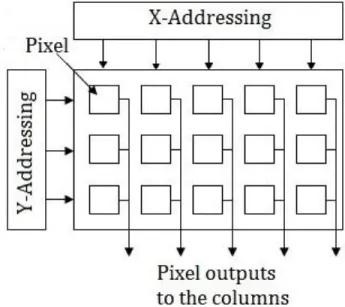
The basic structure of a CMOS image sensor is shown in Figure 1.1. As seen, it contains a two dimensional array of pixels and peripheral circuits. Converting the image into electrical signals is performed by a group of pixels that are arranged in a structure of a rectangular form called array. The number of pixels in an array depends on the complexity and the quality of the sensor. To process signals coming from the pixels, one or more pixels are selected depending on a scanning mechanism. The Y-addressing circuit outputs row control the signal to a row to be selected. The X-addressing circuit scans the sampled signals during the horizontal scanning period [2,15-16]. The pixels in the same column share an output bus into the column in order to reduce the number of connections within the matrix.
Since the array of pixels largely determines the imaging quality of a CMOS sensor [17], it is important to detail the internal structure.
The pixel structure used can be categorized into three types: Passive Pixel Sensor (PPS)
Digital Pixel Sensor (DPS) Active Pixel Sensor (APS)
The structure of a passive pixel is very simple. It is composed of a photodiode connected to the integration node, PD, and a select transistor, as shown in Figure 1.2. Signal amplifier is placed in the column level. The main advantage of PPS is its small pixel size with a large Fill Factor (FF), the ratio of the photodiode area to the pixel area. However, noise injected onto the column readout contributes to noise in the output signal. This Signal to Noise Ratio (SNR) issues halted its development [2,15,17].
Figure 1. 2 Passive pixel
A digital pixel consists of an ADC in addition to the items in PPS. The idea of performing analog-to-digital conversion at pixel level, which led to what was called digital-pixel-sensor, was first introduced by Boyd Fowler [18] in 1994. It offers several advantages. The elimination of column readout noise increases signal to noise ratio. Since the analog-to-digital conversion is performed within each pixel rather than in column or on the chip level, then the conversion error due to device mismatch is reduced.
Another advantage of this pixel sensor is low power consumption. Since the pixel level ADC can work at very low frequency compared to chip level ADC, the total power consumption can be greatly reduced even with each pixel having its own ADC. The main drawbacks of this kind of pixel are a large pixel size and a low fill factor. The integration of analog-to-digital conversion in pixel level increases the number of transistors of each pixel block. High fixed pattern noise is due to threshold voltage variation of pixel level transistors [2,19-20].
A popular implementation of a CMOS image sensor is based on APS. Figure 1.3 shows a basic active pixel structure. In this concept, a photogenerated charge is amplified in a pixel. As shown in Figure 1.3, a typical three-transistor (3T) APS includes a photodiode, a reset transistor, MRS, a source follower transistor, MSF, as a buffer amplifier to isolate the integration node, PD, from the column bus and a row select transistor, MSEL. The source follower is a voltage buffer, which has a current amplification capability. The advantages of the APS because of the added source follower are the increase of speed and the reduction of noise in the signal readout path [2,15-16]. As a result, the APS improves the image quality compared to the PPS.
Figure 1. 3 Voltage mode N-type active pixel architecture
Generally, an APS operation is divided into two main stages, reset and integration. During the reset stage, MRS is turned on and the integration node is reset. Then, MRS is turned off and the integration stage starts. During this stage, the photodiode junction
capacitance is charged at a constant integration time. The voltage of the PD decreases according to the input light intensity and the integration time. This voltage is readout in the column output line by enabling MSEL. When the readout process is finished, MSEL is turned off and MRS is turned on again to repeat the process [16-17].
1.2 Fill
Factor
In order to maximize the quantity of the light absorbed by the pixel, it is important that the circuitry in the pixel takes up as little space as possible. The photodetector should ideally occupy the majority of the pixel area. This is particularly relevant to the sensors that are optimized for high image quality, such as those used in digital still camera applications [15-16]. The fill factor of a pixel is defined as the ratio of the photosensitive area to the total pixel area. The higher the fill factor, the more sensitive the sensor is. The passive pixels have a large fill factor because there is only one transistor in the pixel, while the fill factor of active pixels varies up to about 70% [16-17]. Finally, the digital pixels have the lowest fill factor because of additional transistors required for analog to digital convertor [15-17].
1.3 Image Sensor Characteristics and Performance
There are several characteristics that qualify the performance of a CMOS image sensor. In this section, the principal performance indicators related to the image sensor circuits are introduced.
1.3.1 Dark Current
Dark current is one of the important parameters to characterize the performance of an image sensor. Its behaviour is composed of several contributions. The dark current produced by a photodiode in absence of the light is dominant, especially with long
exposure time [21]. Spatially uniform dark current can be cancelled by subtraction from optical black pixels. However, dark current varies from pixel to pixel and thus the variation reduces the uniformity of the image for low illumination. In order to have the best image quality, the dark current should be extremely low. Dark current is strongly dependent on the temperature and should be taken into account [15]. Dark current also presents a fundamental limit on sensor dynamic range by reducing the signal swing.
1.3.2 Resolution
One of the important aspects of image sensor performance is its resolution. An image sensor is a spatial and temporal sampling device [2]. The resolution of an image sensor is defined as the number of pixels in the array. Assuming a fixed array size, to increase the resolution, the area occupied by a pixel should be reduced. For this purpose we can optimize the layout design, reduce the number of transistors in the pixel and reduce the size of transistors used. Although the spatial resolution increases with the number of pixels in the array, it depends also on the geometry of the pixels and the optical systems used.
1.3.3 Dynamic Range
The dynamic range of a sensor quantifies its ability to acquire scenes with a wide range of illumination. It is usually less than the dynamic range of a scene. The dynamic range of a sensor is particularly limited by the fabrication technology. It is defined by a pixel‟s largest non-saturating photocurrent that it can generate divided by its smallest detectable photocurrent [2,17]. The dynamic range can be simply expressed as:
min max log 20 i i DR , (1.1)
where imax is the maximum non-saturating photocurrent and imin is the minimum detectable photocurrent.
It is important to note that dynamic range is not the same as signal to noise ratio (SNR). The SNR is measured as the ratio between the signal and the noise for a given light intensity, whereas the dynamic range is the ratio between two light intensities. Good dynamic range is necessary to image a scene with the required details and contrast which can be obtained by design optimizations [22]. The human eye has a dynamic range of about 90 dB, however most of the sensors have a dynamic range of about 65-75 dB which is not sufficient for some applications [16-17]. Two methods for dynamic range improvement are considered. One is to reduce the dark current and expand the dynamic range toward darker scenes. The other is to increase the saturation level of the signal and improve the dynamic range toward brighter scenes [23]. Each of them can be achieved by optimizing the electronic circuits. The smallest signal range depends on the noise. So, the dynamic range is indirectly influenced by the noise. It is impossible to increase the dynamic range by increasing the integration time, because the dark current is integrated in the same way [2].
In addition, although using the smaller CMOS technology will increase the fill factor, the lowest supply voltage reduces the dynamic range. Such drawbacks can be alleviated by operating in the current domain. Early circuit design principles and techniques for current-mode processing are becoming powerful tools for the development of high performance analogue circuits and systems. The performance features of current-mode techniques include increased dynamic range and improved linearity, resulting in optimum design [9]. The pixel working in current-mode will be explained later.
The low dynamic range performance of voltage-mode image sensor cannot meet the requirement of many applications. It is desired to have high dynamic range image sensor to distinguish low contrast signal from high background illumination. In order to increase the dynamic range of the standard image sensor, various solutions and methods have been proposed [16,24-28], using a long integration time, a variable integration time and multiple exposures. However, most result in increased pixel area or integration time, decreased resolution, sensitivity or frame rate. One of the solutions to extend the dynamic
range is to compress the response using a logarithmic sensor. Various designs of logarithmic response image sensor have been developed [29-33]. The basic architecture and functionality of this pixel will be explained in the next section.
1.4 Linear Active Pixel Sensor
One of the main components of the sensors is the pixel linear response. Linear operation of the sensor can achieve large output signals and thus a high signal to noise ratio [34]. Figure 1.3 shows the architecture of a general three transistor APS including pixel reset, MRS, source follower amplifier, MSF and row select, MSEL. The pixel is reset by activating φRS, which charges the capacitance of the node PD to voltage near VDD. After switching off the reset transistor, during which the photodiode is exposed to the light, the diode voltage variation, VPD, is linearly dependent on the light intensity. After passing a certain integration time, the charge on the photodiode node, PD, is readout through MSF by switching on MSEL. The pixel output voltage is proportional to the light intensity and the integration time. Then, the pixel is reset again for a new cycle.
The dynamic range of a linear region CMOS pixel sensor is limited; for levels of illumination above a certain limit the capacitance completely discharges during the integration phase. Thus, it is not possible to distinguish differences in the input illumination above this limit, as the output voltage saturates to zero. This results in loss of details in brighter regions. Several techniques have been proposed to improve the dynamic range in [35- 38,61]; however this can be achieved by increasing the number of bits per pixel used to represent the image and multiple sampling techniques, which significantly adds to the cost of the final imager [39]. One of the solutions to increase the dynamic range is to design sensors with a non-linear response that compress the dynamic range of the input signal, which is usually achieved by using pixel operating in logarithmic response as explained in the next section.
1.5 Logarithmic Active Pixel Sensor
The logarithmic (log) APS, introduced around 1983 [40], is essentially a nonlinear readout technique. Its function is a result of the subthreshold operation of a diode-connected MOS transistor, added in series to the photodiode [23]. Pixels in logarithmic mode operate continuously and convert the logarithm of the photocurrent into a corresponding voltage without integration process.
Figure 1.4 shows the basic architecture of a logarithmic APS. This three transistor pixel continuously converts incident light into a voltage that is proportional to the logarithm of the light intensity [41]. This pixel does not require reset and operates continuously. The photocurrent, Iph, is small enough to cause the load transistor, M1, to operate in the subthreshold region. So, the photocurrent, Iph, is equal to the subthreshold current. The VPD is logarithmically dependent on the light intensity, due to the subthreshold operation of M1 [16,23].
Figure 1. 4 Basic logarithmic pixel architecture
The photodiode output voltage is given by the following equation
th D ph DD PD V I I q nKT V V 0 ln , (1.2)
where KT/q represents a thermal voltage depending on the temperature in volt, ID0 is the current at Vth=VGS, and Iph is the photocurrent. n denotes the slope factor given by
ox D C C
n1 , (1.3)
where CD is the capacitance of depletion layer and Cox is the capacitance of the oxide layer.
Any variation in photocurrent will be logarithmically compressed. Then, the dynamic range of the photocurrent will be increased without having to substantially increase the output voltage swing.
Light levels can range from 10-3 lux at night to 105 lux in bright sunlight with the direct viewing of the light source [16]. The advantage of the logarithmic sensors is a simple pixel structure, which has the same number of transistor as a three-transistor APS, while the dynamic range is exponentially increased. In this sensor, ten bits of resolution are sufficient to scene illumination with one percent accuracy for over five decades of luminance. However, to have the same accuracy with a linear sensor, 23 bits are necessary which is not suitable for high speed imaging, data transmission and data storage [22,41]. Another advantage of this technique is to allow for continuous photodiode operation. The photocurrent can be readout anytime and there is no integration involved.
While the logarithmic sensor has the above-mentioned advantages, it suffers from drawbacks such as temperature dependence and low swing of the output, and high fixed pattern noise [16]. The problem of fixed pattern noise is due to the high sensitivity of the MOS subthreshold characteristic to the process variation [23, 41-42]. Also, this form of compression leads to low contrast and loss of details. The response of the logarithmic pixels is light dependent. This means that at low illumination levels, the readout time would be very slow, depending also on the photodiode capacitance, to be able to detect the small currents. Then, in a constant time, the photodiode capacitance is not capable of
being fully depleted. This can lead to image lag and low sensitivity [43]. To alleviate the problem of low light detection, pixels have been designed to operate in combined linear and logarithmic response at low-illumination and high-illumination level respectively. The operating of these combined response pixels will be described in the following sections.
1.6 Image Sensor with Combined Linear-Logarithmic Response
As described in the previous sections, logarithmic response pixels have been used in order to wider dynamic range [23,41]. However, a drawback of these pixels is their limited sensitivity at low light levels [42]. To overcome this disadvantage, the pixels with combined linear and logarithmic response have been proposed [4]. A linear-logarithmic sensor behaves linearly at low light and logarithmically in bright light. A CMOS imager with combined linear-logarithmic operation has been proposed by [43], as shown in Figure 1.5. The operation is explained as follows [42]. The photodiode resets to a voltage Vbias that is higher than VDD so that when φRS is high, VPD is biased to a voltage which is less than the voltage required for sub-threshold conduction across the transistor M1. Photocurrent produced across the diode will cause to decrease VPD linearly until it reaches to point where sub-threshold conduction occurs. Beyond that point, VPD will vary logarithmically. If the illumination is low, the VPD will not saturate within the integration time. Then the pixel output will response like a three-transistor APS, so called linear operation. However, if the illumination is high, the photodiode will soon become saturated and the VPD will put M1 into sub-threshold region, operating the pixel in logarithmic mode response. Linear integration mode operation of the sensor can achieve large output signals and thus a high signal to noise ratio. On the other hand, the logarithmic mode of the pixel operation allows a wide dynamic range [34].
Figure 1. 5 Schematic of a linear-logarithmic pixel
The linear range is adjustable through Vbias so that the larger the offset between VDD and Vbias, the greater the width of the linear region. This method combines the advantages of linear and logarithmic pixels with a smooth transition between the two modes of response. Then, a dynamic range of over 100dB can be obtained [44-46,62].
1.7 Current-Mode Response Image Sensor
The majority of the reported image sensors are implemented in voltage-mode [3,5-8]. As technology scales down, it necessitates the reduction of supply voltage to reduce the power dissipation. However, the reduction of supply voltage leads to a degraded circuit performance in terms of signal swing, signal to noise ratio and dynamic range [9-10].
In current-mode image sensors, the signal swing is not affected by such trends. Also, they need less silicon area and have higher operation speed [47]. A current-mode APS provides an alternative to the traditional voltage mode.
Figure 1. 6 Current-mode image sensor
Figure 1.6 shows the architecture of a current-mode image sensor. It is composed of a photodiode, a reset transistor M1, an active device M2, and a row select transistor, M3. In current-mode pixels, the output voltage in the column bus is fixed. So, it prevents from charging and discharging the column capacitance during readout to maximise the operating speed [10-11,46].
Many current-mode imaging structures have suffered from high Fixed Pattern Noise (FPN) due to device parameter variation and have nonlinear transfer characteristics which have limited the effectiveness of noise suppression circuitry [10-11,13-14]. Active device transistor, M2, operates in the triode region to convert the photovoltage, VPD, to an output current, Ipixelout, linearly. For pixel operating in current mode, the column readout circuits work in the current domain.
1.8 Conclusion
In this chapter, we had an overview on the basic CMOS image sensors. The various possible structure of pixels used in sensors was presented. In order to characterize the
CMOS image sensor performance, we introduced its performance indicators. Then, we explained about the current-mode technique and its advantages.
In this thesis a linear-logarithmic active pixel sensor operating in current mode is designed. A high dynamic range is achieved by pixel in both linear and logarithmic modes of operation. If the pixel in the linear image saturates, it is replaced by a corresponding logarithmic operation without the need for a frame memory. In addition, in current-mode pixels, the column bus voltage is fixed. So, a change in the current level through a node is not necessarily accompanied by a change in the voltage level at that node. Hence, parasitic capacitance would not degrade the operating speed. Also, using current-mode have reduces the power consumption because even if the power supply voltage is low, the required dynamic range is achieved. Based on these advantages, we can conclude that it is useful to design our image sensor in linear-logarithmic operation using the CMOS current-mode technology. Next, chapter 2 presents the architecture of a linear-logarithmic APS having a current-mode output.
CHAPTER 2
DESIGN OF IMAGE SENSOR AND READOUT CIRCUIT
2.1 Introduction and Design
Chapter 1 introduced the physical structure of image sensors and their functionality. Based on these concepts, this chapter describes the design steps of the image sensor and readout circuit in detail. The objective of designing the image sensor is to increase the dynamic range. As mentioned in Chapter 1, using current-mode because of the reduction of supply voltage in the shrink size CMOS devices has the advantage of high dynamic range. In addition, the image sensors operating in the combine mode of linear-logarithmic has improved dynamic range compare to the sensors operating in a single mode. Then, in this design, we use the current-mode linear-logarithmic image sensor to have the operating response with high dynamic range. Accordingly, all the circuit in the column are designed in current-mode which is compatible with the image sensor.
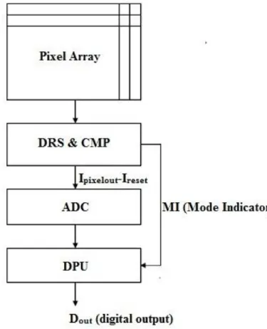
Figure 2.1 shows the block diagram of the proposed imaging system, working on current mode.
Figure 2. 1 Current-mode imaging system architecture
As mentioned in chapter 1, the designed pixel operates in current-mode with linear-logarithmic response. At the end of the integration time of the pixel, two successive pixel output currents are sampled by the Delta Reset Sampling (DRS) to determine the operating mode response of the pixel. Two roughly similar samples indicate that the pixel is in the logarithmic mode. The response mode is detected by the comparator, CMP. After the reset phase, another sample is sent to the DRS to reduce the FPN and the image lag effect. The current mode DRS sends an offset free current to the current mode analog to digital convertor. The corrected output current is independent of the voltage threshold variations of the pixel read out transistor [13]. The comparator Mode Indicator flag (MI) indicates to the Digital Processing Unit (DPU) when the pixel is operating in the logarithmic mode so that the ADC digital output is converted accordingly.
In the following sections, we will describe the architecture and functionality of the designed pixel sensor and then the related readout circuits. We will discuss about the causes of non-linear output current transfer characteristic and develop an analytical solution that can be implemented in the digital domain.
2.2 Pixel Architecture and Operation
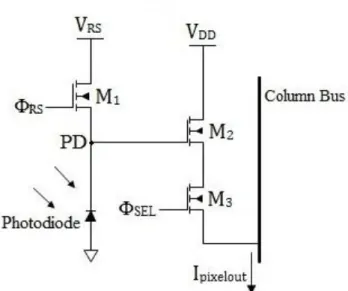
The proposed three-transistor pixel architecture is shown in Figure 2.2.
Figure 2. 2 Proposed pixel architecture
The pixel consists of a photodiode, a diode connected transistor M1p, transistor M2p operating in the linear region and a row select switch M3p to connect the pixel to the column bus. The integration voltage, VPD, is converted to an output current, Ipixelout, by transistor M2p, acting as a transconductance amplifier. In order to increase the dynamic range, the active pixel has been designed in current-mode with a linear-logarithmic response. In current mode pixels, the fixed output voltage Vref prevents from charging and discharging the column capacitance during readout to maximise the operating speed [10]. The drain voltage of M2p should not be far from VDD to ensure that M2p is in the linear region. Under the assumption that Vref is constant, the drain voltage of M2p is
approximately equal to Vref. So, Vref must be close to VDD. The transconductance Gpix, given by (2.1), is approximately linear;
DD ref
p p ox p PD pixelout pix V V L W C V I G 2 2 2 . (2.1)Select switch M3p connects pixel to the output bus. Ideally, M3p has zero on-resistance; meaning that the voltage drop across is 0V. This approximation seen in (2.1) becomes less valid at low supply voltages. The finite on-resistance of M3p produces non-linear effects. The analytical solution for this effect is provided in the next section.
The bias voltage, VS, determines through transistor M1p the pixel reset-integration phase. The VSL and VSH indicate the low and high level of the bias voltage, VS, respectively. VSH is chosen to ensure that the gate voltage of M2p is enough to remain „on‟ during the reset phase. VSL is selected to set the photodiode current at which the pixel operating mode changes from linear to logarithmic, during the integration time. So, to ensure that M2p is always above threshold:
thp DD
S V V
V . (2.2)
The pixel shown in Figure 2.2 operates as follows. At the end of the reset, after charging up the node capacitance CPD through the reset transistor M1p, the photodiode is exposed to the incident light during integration time. It generates the photocurrent Iph that discharges CPD. Then, the photodiode voltage VPD decreases proportionally to the light intensity and the integration time tint.
In the case where the light intensity is not sufficiently strong to decrease VPD substantially, M1p remains in the cut off region. So, the voltage of the photodiode VPD is linearly dependent on the light intensity. It is given by
int 1 t ph PD PD I dt C V . (2.3)For high intensity incident light, VPD becomes logarithmically dependent on the light intensity, due to the subthreshold operation of the diode connected, M1p, transistor. It is expressed as the equation (1.2), explained in Chapter 1.
The transistor M2p being in linear mode of operation will output a current, Ipixelout, linearly proportional to VPD, as described by the following equation:
2 2 , , 2 2 2 2 2 p M DS M DS th GS p p ox p pixelout V V V V L W C I p , (2.4)where µ2p is the hole mobility, Cox is the oxide capacitance, Vth is the threshold voltage, W2p and L2p are the transistor‟s width and length and VGS is VPD-VDD.
This linearity allows for easy suppression of the variations, appearing as fixed pattern noise, using a current mode delta reset on the column circuit.
Figure 1.A, in Appendix, shows the layout view of the pixel with the labelling of the transistors and inputs. In this design, we have chosen traditional n-well/p-substrate photodiode as photo-detector. This kind of photodiode has relatively good performance compared to other traditional photodiode implementations. Also, it has much lower leakage current and higher sensitivity to visible light compare to n+/p-substrate photodiode. In this layout, the light sensitive area is 53.28μm2 in which the total area of the pixel is 144 μm2. So, the fill factor calculated as the percentage of the ratio of these two values is 37%.
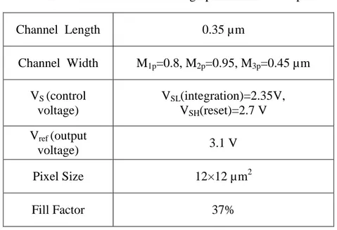
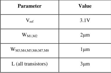
Table 2.1 shows the design parameters and characteristics of the pixel. For all the three transistors, the minimum channel length is used. The VSL and VSH are determined as mentioned above. Also, the column reference voltage, Vref, is set up to the value to keep the transistor M2p in linear region as explained before.
Pixel
Table 2. 1 Characteristics and design parameters of the pixel Channel Length 0.35 µm Channel Width M1p=0.8, M2p=0.95, M3p=0.45 µm VS (control voltage) VSL(integration)=2.35V, VSH(reset)=2.7 V Vref (output voltage) 3.1 V Pixel Size 12×12 µm2 Fill Factor 37%
2.2.1 Pixel Non-linearitiy Analysis
Figure 2.3 shows the output current as a function of time for the linear operating response of the pixel. As it is shown, the different curves are for different widths of the transistor M3p. It can be noticed that the output is not completely linear. The simulation proves that increasing its width even as high as ten times does not solve the linearity problem while increasing dramatically the pixel area.
A first degree contribution to this nonlinearity is the „‟on‟‟ resistance of the select transistor, M3p, which exhibits an increasing drain-source voltage drop as the output current increases. To eliminate the effect caused by M3p „on‟ resistance, Ron, we rely on the digital domain after ADC conversion to apply a linearization function.
Figure 2. 3 Simulated linear current response for different width of M3p
Another non-linearity effect comes from the variation of the photodiode voltage as a function of time, as shown in Figure 2.4. Since the technology used for chip design does not offer photodiode model, the schematic level simulation have to be carried out using a simplified photodiode model that was approximated as a capacitor in parallel with an ideal current source to discharge the diode capacitance. It is suspected that the slight nonlinearity comes from the photodiode capacitance variation as a function of VPD.
Another cause of non-linearity is the hole mobility degradation of transistor M2p as a function of VGS. It has also been recognized as an important source of non-linearity for current-mode active pixel [10,13,48].
Figure 2. 4 Simulated photodiode voltage variations as a function of time
2.2.2 Analytical Solution
To remove the non-linearity effect coming from the Ron, we use an analytical solution
that can be implemented in the digital domain [46]. The transistor M2p works in the linear region, so the relationship between its output current and its gate voltage, VPD is linear as shown in equation (2.4). The square term is neglected as
p
M DS V
2
, has a small value. From
Figure 2.2, we have: pixelout on M DS ref DD V V R I V p 2 , . (2.5)
In ideal case, assuming that the pixel output current is linear and there is no voltage drop over Ron, VDS,M2pis equal to 0.2V. According to the equation (2.4) we have:
0.2 2 2 2 th GS p p ox p lin V V L W C I , (2.6)in which the last term of the equation is neglected.
Deducing p M DS V 2
, from both of the equation (2.4) and (2.5), and replacing VDD-Vref by
0.2V, we have the following equation
GS th
on pixelout p p ox p pixelout I R V V L W C I 2 . 0 2 2 2 . (2.7)Using the last two equations results in the linearization function for a non-negligible Ron as in the following pixelout on pixeloout lin I R I I 5 1 . (2.8)
This correction can be performed numerically by the digital processing unit. Also, we can use the geometric series to obtain approximately the same result as the fractional form. It is therefore easier to implement in digital circuit than the fractional form. The geometric series of the equation (2.8) will be as the following
n n pixelout on pixelout pixelout on pixelout I R I I R I
0 5 5 1 ,for 5RonIpixelout 1 . (2.9)The condition will be satisfied since the Ron is on the order of ohms and Ipixelout is on the order of micro-ampere.
Before digitizing the analog current Ipixelout, a current memory performing a Delta Reset is employed to remove the FPN due to variations of transistors M1p and M2p threshold
voltage [28]. Therefore the output current converted by the current mode ADC is Iout-Ireset. In the context of an ASIC CMOS sensor with on-chip ADC and digital processing, the linearization function (2.8) must be realized effectively with an easy to implement arithmetic logic unit.
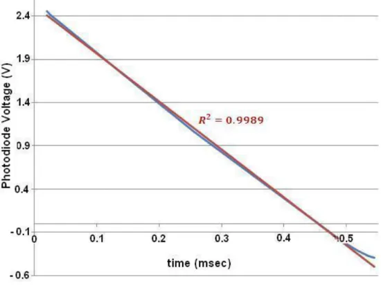
Figure 2. 5 Experimental results of the linearized pixel output current
Figure 2.5 shows the linearized experimental results with both fractional equation (2.8) with a residue of 0.9902, and its geometric series, equation (2.9). A geometric series of 16 terms must be used to obtain approximately the same result as the fractional form. However for an ADC of up to 10 bits, a lookup table could also be used with the advantage of a higher conversion rate. This result obtained when VSL set to zero. Then, the pixel operates in the linear mode response and depending the light intensity it saturates after passing time.
According to the Figure 2.2, when the light intensity increases, the photodiode voltage, VPD, decreases. The maximum pixel output current, Ipixelout, is obtained when the forwarding bias current of the photodiode is equal to Iph, according to the photodiode
characteristic. After that VPD remains constant and the Ipixelout is constant as well. In the Figure 2.5, it is seen that Ipixelout is starting to decrease. This behaviour comes from the threshold voltage temperature dependence of M1p and M2p which affects directly the output current [49]. This part of the output characteristics cannot be linearized using our simple mathematical solution.
2.3 Current-Mode Column Readout Circuits
This section describes the design of the column readout circuit for a current-mode linear-logarithmic pixel. The design includes the circuits required to copy the output current of the pixel into the column, to remove the offset and to determine the operating mode of the pixel. After photocurrent integration in the pixel, readout is performed by transferring the pixel output current to the column circuit. One of the important circuits in the column is a delta reset sampling used to cancel device parameter variations. A current conveyor is used to fix the pixel output voltage and provide a copy of the pixel output current [10].
2.3.1 Current Conveyor
The first part of readout circuitry in current-mode pixels is a current conveyor circuit. The concept of current conveyor is the current conveyed between two ports at different impedance levels [50]. It was initially proposed by Smith and Sedra in 1968 [51-52]. The current conveyor offers several advantages over the conventional opamp. It can provide a higher voltage gain over a larger signal bandwidth under small or large signal conditions [9].
Figure 2.6 represents a block box of current conveyor. If one of the input terminals is connected to a voltage, an equal voltage will appear on the other input terminal. In a dual manner, if a current is applied through one input, an equal current will flow through another input and the same current is conveyed through output terminal. Its operation is
explained in [9,50]. The potential of X, vX, being set by vY is independent of the current being forced into port X. Similarly, the current through input Y, iY, being fixed by iX is independent of the voltage applied at Y.
Figure 2. 6 Basic block diagram of a current conveyor
Current conveyor can be applied in a variety of analog circuits. It can be used to have a fixed voltage node and to copy the input signal as shown in Figure 2.7 for the first generation Current Conveyor (CCI). Assuming that transistors M3-M5 are matched, it can be shown that the currents through them are equal. This forces transistors M1 and M2 to have equal currents and thus equal VGS drops. Thus X and Y track each other in both voltage and current.
Figure 2. 7 CMOS implementation of CCI
vX X Z vY Y IX IY IZ
Figure 2. 8 Current conveyor
In this design, we use the cascoded current conveyor, adding the transistors M6-M8, as shown in Figure 2.8. This architecture reduces the channel length modulation, and the output current is more precise. We connect the first branch, Y, into an external biasing voltage as Vref. The next branch, X, is connected to the pixel output. Then, the voltage of the column bus will be the same as Vref. Accordingly, the pixel output current will be copied in the branch Z by adjusting the transistors dimensions as in Table 2.2, so that IZ is equal to Ipixelout.
Table 2. 2 Parameters values of the current conveyor circuit
Parameter Value
Vref 3.1V
WM1,M2 2μm
WM3,M4,M5,M6,M7,M8 1μm
2.3.2 Current-Mode Offset Cancellation Circuit
A common approach used in voltage mode active pixel sensors is to eliminate offset caused by random variations in the threshold voltage of the pixel transistors with Correlated Double Sampling (CDS). The CDS circuit, usually located at the bottom of each column, subtracts the reset value from the signal pixel value [16]. In current mode active pixel sensors a DRS circuit is used as an offset suppression circuitry. It is implemented in a switched-current memory cell shown in Figure 2.9.
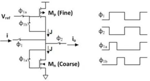
Figure 2. 9 Basic two-step sampling current memory cell
Error cancellation is achieved by switches through a non-overlapping two-step sampling process. In this so-called S2I memory cell [53], the signal is sampled by the NMOS memory, Mn, during the first (coarse) step, φ1a. When the cell has settled, all of the signal current together with the bias current, J, flows into the coarse memory. Then, during the second (fine) step, φ1b, the error is sampled and stored in the PMOS memory, Mp, while the bias current flows through the transistors. On the output phase, the subtraction of these two signals appears at the output which is also free of the bias current.
The applications for current systems will be much the same as for switched-capacitors. Linear floating capacitors are not needed in switched-current circuits. In principle, voltage swings need not to be large as signals are represented by currents [9].
Figure 2. 10 a) Proposed switched-current memory cell (DRS) b) Clock waveforms
Figure 2.10 a) shows the modified current memory cell working as delta reset sampling circuit, different from the basic one. It is connected to the designed current conveyor, node Z of the Figure 2.8, in which the pixel output current passes. The incoming current of the DRS, Ipixelout, is controlled by SEL switch which is in the pixel, Figure 2.2.
In this design, M11 operates as the coarse memory while M22, which is cascoded with M21 to reduce the effect of channel length modulation, works as the fine memory. The error of channel length modulation created by M11 will be removed from fine memory in subtraction cycle. Then, we only use the cascode version for the fine part. The width of cascode transistor M21 is adjusted to minimise the drain-source voltage of M22, while adjusting Vbias to ensure that the transistor is saturated in the range of the input current. The clock waveforms are shown in Figure 2.10 b). The select switch transistor located in the pixel, Figure 2.2, acts as the input switch for the DRS circuit. While the select signal is low, the two sampling of coarse and fine memory are done respectively.
In our work, the design procedure was adopted for optimizing the cell performance as shown in Table 2.3. In memory cell design, transistor sizing is a very important procedure to get behaviour close to optimum performance.
Table 2. 3 Parameters designed values Parameter Value WM11 3.2μm WM21 2.0μm WM22 1.0μm L (all transistors) 9.0μm
2.4 Mode Indicator Circuits
In order to determine the operating mode of the pixel, we need a circuit block to detect the pixel output current and recognize its operating mode. For this purpose a current comparator circuit is needed to compare two successive currents. If these two currents are similar, then the pixel is in the logarithmic mode of operation. Otherwise, it is in the linear operating mode. However, these sampled current must be kept in order to be compared. Consequently, we introduce an integrator with capacitive feedbacks before the comparator circuit. The functionality of each circuit is explained in the following sections.
2.4.1 Integrator
This block consists of a simple one stage fully differential amplifier with Common Mode Feedback (CMFB). A differential feedback loop with high loop gain is used to control the common mode output voltage [54]. Figure 2.11 shows the schematic of the circuit.
Figure 2. 11 One stage fully differential amplifier with CMFB
The simple fully differential amplifier consists of a differential pair MN1-MN2, active loads MP3 and MP4, and tail current sources MN3 and MN4. For the op-amp, an ideal operating point biases MN1-MN4 and MP3-MP4 in the active region and sets the DC common mode (CM) output voltage, VOC, to the value that maximizes the swing at the op-amp outputs for which all transistors operate in the active region. However, VOC is very sensitive to mismatch and component parameter variations, so that accurately setting it to a desired voltage is impossible in practice. To set VOC to a desired DC voltage that biases all transistors in the active region and maximizes the output voltage swing, either Vbiasp or VGS-MN3 must be adjusted. Adjusting VGS-MN3 to force VOC=VCM requires the use of feedback in practice which will be referred to as the common-mode feedback (CMFB). A straightforward way to detect the common-mode (CM) output is to use two equal resistors [54], R0 and R1, as shown in Figure 2.11. This CMFB uses resistive divider and a modified CM sense amplifier that injects currents into the opamp to control the opamp CM output voltage. The voltage between the two resistors is
2 2 1 o o oc V V V . (2.10)This modified CM-sense amplifier directly injects currents to control the opamp CM output. The dimensions of the transistors are shown in Table 2.4. The current injected by MP0 and MP1 into either output is
oc CM
MP m MP cms V V g I I 2 4 0 5 . (2.11)Transistors MN3,MN4, MP3 and MP4 act as current sources. The CMFB loop will adjust Icms so that: 4 3 4 3 D MP 2 cms D MN D MN MP D I I I I I . (2.12)
If Voc=VCM, MP0, MP1, and MP2 give 2Icms=IMP5/2. Therefore, IMP5 should be chosen so that: 4 3 5 4 3 2 D MN D MN MP MP D MP D I I I I I , (2.13)
when all devices are active. Accordingly, in the CM-sense circuit, (W/L)MP0=(W/L)MP1=0.5(W/L)MP2. Table 2.4 shows the design parameters and transistors dimensions in order to operate the differential amplifier with common-mode feedback properly.
Table 2. 4 Transistor‟s parameter values of the differential amplifier with CMFB
Parameter Value Parameter Value
WMP3,4 5.0μm WMP5 11.2μm LMP3,4 0.7μm LMP5 3.0μm WMN1,2 6.4μm WMP0,1 4.0μm LMN1,2,3,4 2.0μm LMP0,1,2 2.0μm WMN3,4 11.4μm WMP2 8.0μm Vbiasp 2.3V R0,1 200KΩ Vbiasn 0.7V
Capacitors are then introduced between the inputs and outputs to sample the current coming from the DRS circuit. Figure 2.12 shows the integrator.
Figure 2. 12 Differential integrator
In this circuit, we used two switches, Fo1 and Fo2, in order to transfer the sampled current coming from DRS circuit. During each phase of input Fo1 or Fo2, one is connected to the IoDRS, while the other input is connected to the common mode voltage, VCM. The current sampled creates voltages across capacitors C1 and C2. The switches P1 and P2 reset the capacitors before starting the output phases, so the inputs and outputs of the integrator are on a common mode voltage level.
First, switches P1 and P2 are closed and the capacitors are reset. Then, we open them and the first sample charges up C1 during Fo1. During this time, C2 charges at the same rate as
C1. Due to the CMFB, while O1 is decreases, O2 increases, so the average output remains VCM. During Fo2, the second current sampled discharges C2 and C1. If the second sample is larger than the first one, the slope of the discharge will be greater. In this case, the pixel operates in linear mode response. Otherwise, the second sample is similar to or smaller than the first one when the pixel is in the logarithmic response.
a)
b)
Figure 2. 13 Integrator output for the pixel operating in a) linear operating mode and b) logarithmic operating mode
Figure 2.13 a) and b) shows the simulation results of these two conditions, respectively. As seen, in the linear operating mode of the pixel, at the end of the stage Fo2, O1 is greater than O2 while in the logarithmic response O1 is smaller than O2. The constant output values appearing before Fo1 pulse and after Fo2 pulse are fixed by the CMFB at 1.65V. The maximum and minimum values of output voltage at the end of a current sampling are limited by the op-amp dynamic range which is approximately 1.3V.
Figure 2.14 shows the output swing of the differential amplifier with CMFB. One of the inputs sets to 1.65V while the other sweeps from 0V to 3.3V. The differential output varies from 1.074V to 2.375V.
Figure 2. 14 Output swing of the differential amplifier
Figure 2.A, in Appendix, shows the layout view of the integrator. We use inter-digitization finger technique to improve transistor matching in the differential pair and the CM amplifier, and also common centroid structures to improve matching between components in the layout. The resistors are implemented by n-well layer.
2.4.2 Comparator
Comparators are widely used in many analog circuits. The low power comparator operation is based on a positive feedback loop of two back-to-back inverters in order to convert a small input-voltage difference to a full scale digital level in a short time. Its operation is controlled by clock signal pulses. When the clock is low (reset phase), the output node is reset to VDD. During the reset phase of the comparator and after it has finished regeneration, there is no supply current [55-56].
There is a large variety of CMOS latched comparators. One of them is static latched comparator in which the regeneration is done by two class A cross-coupled inverters. These comparators are always consuming current even after regeneration therefore; it is not attractive for low power operation [57]. Another type of comparators are more power efficient than the static comparators [58]. However, there is still supply current in the reset phase and after the comparator has finished regeneration. In the dynamic latched comparators, there is only current flowing during the regeneration [58-59]. Figure 2.15 shows the schematic diagram of a dynamic latched comparator.
The differential pair transistors, MN11 and MN12, are input transistors. MN14/MP12 and MN15/MP11 compose a latch structure. MN13 is used for power reduction and the other transistors are used for reset. The comparator is controlled by a single clock phase. During the reset phase, when clock is low, transistors MP13/MP14 and MP17/MP16 reset the output nodes and drains of the MN11/MN12 to VDD. MN13 is off and no supply current exists. When the clock goes high, the reset transistors are opened and the current starts flowing in MN13 and in the differential pair. Depending on the input voltage, one of the cross-coupled inverter that makes the regeneration, MN14/MP12 or MN15/MP11, receives more current and determines the final output state. After regeneration is completed, one of the output nodes is at VDD, and the other output and both drains of the differential pair are at 0V. In this situation, there is no supply current, which maximizes the power efficiency [58-59].
Figure 2. 15 Dynamic latched comparator
According to the pixel response, when it is in linear operating mode, the two successive currents are different and the first one is smaller than the second one. So, the comparator output should be “1”. However, in the logarithmic mode of operation, these currents are sometimes equal or the second current sampled is smaller than the first one. In this state, the comparator output changes to “0”. These normal operating states of the comparator can be altered by the mismatch resulting from variations of the fabrication process, which deteriorates the accuracy of the comparator.