UNIVERSITÉ DE MONTRÉAL
A NOVEL CMOS MICRO-SPECTROMETER BASED ON WAVELENGTH ABSORPTION
KAI ZHANG
DÉPARTEMENT DE GÉNIE ÉLECTRIQUE ÉCOLE POLYTECHNIQUE DE MONTRÉAL
MÉMOIRE PRÉSENTÉEN VUE DE L’OBTENTION DU DIPLÔME DE MAÎTRISE ÈS SCIENCES APPLIQUÉES
(GÉNIE ÉLECTRIQUE) AOÛT 2017
UNIVERSITÉ DE MONTRÉAL
ÉCOLE POLYTECHNIQUE DE MONTRÉAL
Ce mémoire intitulé:
A NOVEL CMOS MICRO-SPECTROMETER BASED ON WAVELENGTH ABSORPTION
présenté par: ZHANG Kai
en vue de l’obtention du diplôme de : Maîtrise ès Sciences Appliquées a été dûment accepté par le jury d’examen constitué de :
M. SAVARIA Yvon, Ph. D., président
M. AUDET Yves, Ph. D., membre et directeur de recherche M. SIROIS Frédéric, Ph. D., membre
DEDICATION
To my parents, who love me and support me all the time. To my father, may you rest in peace.
ACKNOWLEDGEMENTS
In the past years, I struggled and fought for my project. After countless failures, dawn finally comes. I would like to take the hard-earned opportunity to thank various people who helped me to complete this achievement.
First of all, I would like to express my deep gratitude and appreciation to my research supervisor, Prof. Yves Audet, for providing continued support throughout my entire program. Thanks to his profound knowledge in semiconductor device and electric circuits, as well as his great patience at all times. The memory of many nights, we discussed the problems until midnight, is precious and unforgettable. Without his generous help and wise guidance, I would not have finished my thesis.
I must thank the past and current colleagues in Groupe de Recherche en Microélectronique
et Microsystèms at Polytechnique Montréal, Jacques Girardin, Réjean Lepage, Jean Bouchard,
Bryan Tremblay, and especially Pascal Burasa, whose excellent work provides me a solid basis to develop the spectrometer.
I sincerely acknowledge China Scholarship Council, for offering me three-year scholarship, and giving me the opportunity to study in Canada.
I will thank all my friends, who helped me to survive in the most difficult time.
At the end, I’d like to devote this work to my parents. My father passed away because of cancer in 2010 while I was studying in Canada. My mother took care of my father and shouldered all family burden by herself during those years. No words could express how much love and appreciation to them.
RÉSUMÉ
L'analyse spectrométrique est une technique largement utilisée pour étudier les matériaux et les composés. Les spectromètres modernes dédiés à la recherche sont des instruments encombrants composés d’une source lumineuse, d’un élément de dispersion, de lentilles, d’un capteur photonique, de composants électromécaniques et de circuits électroniques de contrôle, de traitement de données et de mémoire. Les éléments de dispersion les plus couramment employés sont les prismes et les réseaux de diffraction ou d’interférence. Les éléments de dispersion sont irremplaçables dans les spectromètres modernes.
Dans cette thèse, une nouvelle méthode pour la détection du spectre basée sur l’absorption des photons dans le Silicium, matériau de base employé dans les procédés de fabrication microélectronique, est proposée. Le spectromètre, nommé Wavelength Absorption Spectrometer (WAS), n’utilise aucun élément de dispersion. Les technologies de fabrication CMOS permettent d’implémenter sur la même puce, le détecteur et les composants de traitement de signal du spectromètre.
La profondeur de pénétration de la lumière incidente dépend de la longueur d’onde pour un matériau semi-conducteur spécifique de sorte que l’information spectrale peut être obtenue en mesurant la concentration en excès de paires électron-trou photo générés en fonction de la profondeur. Le transport des charges en excès photo-générées dépend de la concentration des dopants, de la distribution des champs électrique et magnétique, du taux de génération et de recombinaison, de la vitesse de recombinaison de surface, de la durée de vie des charges, de la température et de la géométrie du dispositif.
La thèse traite en détail le principe de détection proposé et présente les résultats expérimentaux d'un prototype WAS. Trois longueurs d’onde, 470 𝑛m, 530 𝑛m et 640 𝑛m, avec plusieurs irradiances, sont utilisées afin de vérifier le principe de détection utilisant un champ magnétique externe. Lorsque la concentration du transporteur est élevée, les résultats expérimentaux confirment l'analyse théorique que la longueur d'onde devient indiscernable, car le mécanisme de recombinaison Auger est dominant. Un modèle d'éléments finis confirme le principe de détection
des trous en excès en fonction de la profondeur où la trajectoire des trous en mouvement est déviée sous la force de Lorentz vers un ensemble de collecteurs. Afin de réaliser le spectromètre, une méthode de détection du spectre lumineux est développée, ce qui nécessite un ensemble d'équations linéaires où les coefficients de la matrice proviennent de la mesure de la densité de courant en fonction de l'irradiance pour différentes longueurs d'ondes et champs magnétiques.
Différent du spectromètre traditionnel, la résolution de WAS dépend des courants détectables minimaux de trou. Le calcul théorique prédit que la résolution du WAS se situe au environ de 219 selon le niveau de bruit provenant des jonctions de collecteurs.
Afin de développer un spectromètre plus compact et peu coûteux, deux prototypes sont modélisés où le principe de détection ne requiert aucune génération de champ magnétique. Cependant, la faible résolution est un inconvénient principal de ces structures modifiées.
ABSTRACT
Spectrometry analysis is a widely used technique to investigate materials and structures. The current research-grade spectrometers are bulky equipment composed of a light source, a dispersing element, lenses, an optical sensor, electromechanical components and an electronic circuit. The commonly used dispersing elements mainly include a prism, diffraction grating, or an interference component. The dispersing elements are irreplaceable in modern spectrometers.
In this thesis, a novel method of detecting the spectrum based on wavelength absorption phenomenon in silicon is proposed; it is called Wavelength Absorption Spectrometer (WAS). CMOS integrated circuit technology is highly mature and allows the detector and the signal processing component to be implemented on the same chip.
The light incident depth depends on its wavelength for a specific semiconductor material, thus the wavelength spectral information is obtained by measuring the photo-generated electron-hole pairs as a function of depth. Under the electric and magnetic field, the photo-generated holes are collected by reverse-biased PN junctions. The excess carrier transportation depends on the doping concentration, the electric and magnetic field distribution, the generation-recombination rate, the surface recombination velocity, carriers' life time, the temperature, and the device geometry. All of these factors are discussed in the thesis.
The thesis discusses the proposed detection principle in detail and presents experimental results of a WAS prototype. Three wavelengths, 470 𝑛m, 530 𝑛m and 640 𝑛m, with several irradiances, are used to test the prototype under a varying external magnetic field. When the carrier concentration is high, experimental results confirm the theoretical analysis that wavelength becomes indistinguishable because the Auger recombination mechanism is dominant. A finite element model confirms the excess holes’ detection principle as a function of depth where moving holes’ trajectory is deviated under the Lorentz force towards a set of collectors. In order to realize a spectrometer, a light spectrum detection method is developed, which requires a linear equation set where coefficients of the matrix come from the measurement of the current density as a function of the irradiance for different wavelengths and magnetic fields.
Different from the traditional spectrometer, the resolution of WAS depends on the minimal detectable current of excess holes. The theoretical calculation predicts that the resolution of the WAS could reach around 219 depending on the collectors’ junction shot noise.
In order to develop a more compact spectrometer, two models are conceived where the detection principle does not rely on space-consuming magnets. However, the low resolution is the main disadvantage of these modified structures.
TABLE OF CONTENTS
DEDICATION ... iii ACKNOWLEDGEMENTS ... iv RÉSUMÉ ... v ABSTRACT ... vii TABLE OF CONTENTS ... ixLIST OF FIGURES ... xii
LIST OF SYMBOLS AND ABBREVIATIONS... xv
LIST OF APPENDICES ... xvi
CHAPTER 1 INTRODUCTION ... 1
1.1 General Background ... 1
1.2 Objectives of the Project ... 1
1.3 Contributions of the Thesis ... 2
1.4 Structure of the thesis ... 3
CHAPTER 2 LITERATURE REVIEW ... 4
2.1 Optical Absorption ... 4
2.2 Generation and Recombination ... 5
2.3 CCD and CMOS Detector ... 5
2.4 Hall Effect ... 6
2.5 State of the Art in Spectrometry ... 7
2.6 Recent development on filter-less optical sensor ... 11
2.7 Miniaturized spectrometer ... 14
CHAPTER 3 A NOVEL CMOS SPECTROMETER BASED ON WAVELENGTH
ABSORPTIOION ... 16
3.1 Abstract ... 16
3.2 Introduction ... 16
3.3 Detection Principle ... 17
3.3.1 The excess holes’ generation and recombination ... 19
3.3.2 The excess holes’ transportation under magnetic field ... 21
3.3.3 Experiment details and data analysis ... 26
3.4 Application as a spectrometer ... 31
3.5 Conclusion ... 33
CHAPTER 4 RESOLUTION ANALYSIS ... 35
4.1 Definition of Resolution ... 35
4.2 The resolution of the WAS ... 35
4.3 Conclusion ... 39
CHAPTER 5 SOLUTION OF CONTINUITY EQUATION ... 40
5.1 Boundary conditions ... 40
5.2 Surface recombination velocity ... 42
5.3 Carriers lifetime ... 43
5.3.1 Constant Lifetime ... 45
5.3.2 Variable Lifetime ... 49
5.4 Conclusion ... 50
CHAPTER 6 FINITE ELEMENT METHOD MODELING ... 51
6.1 Model Setup ... 51
6.2 Improved Models ... 57
6.2.2 The various depths of P1 collector ... 62
6.3 Conclusion ... 64
CHAPTER 7 CONCLUSION AND FUTURE WORK ... 66
7.1 Summary ... 66
7.2 Contributions ... 67
7.3 Suggestions for future work ... 67
BIBLIOGRAPHY ... 68
LIST OF FIGURES
Figure 2-1 Absorption of photon flux in silicon. ... 4
Figure 2-2 Absorption coefficient vs wavelength in silicon. ... 5
Figure 2-3 The schematic figure of Hall Effect and Lorentz force in a semiconductor... 6
Figure 2-4 Light is dispersed by a prism. ... 8
Figure 2-5 Diagram of reflective diffraction grating principle [24]. ... 9
Figure 2-6 Schematic diagram of Michelson interferometer principle [25]. ... 10
Figure 2-7 Formation of fringes in a Michelson interferometer [26]. ... 10
Figure 2-8 Diagram of the Foveon sensor. ... 11
Figure 2-9 TFD simulation result. The streamlines show the electric field. The contact n1 collects the electrons to depth X1, contacts n2 collect electrons to depth X2, and collectors n3 collect other electrons generated in other region. [30] [Year 2009 of original publication]. ... 12
Figure 2-10 Schematic of sensor pixel and readout circuit [31]. Reprinted with permission from Elsevier. ... 13
Figure 2-11 Operation of the filter-less fluorescence sensor [31]. Reprinted with permission from Elsevier. ... 13
Figure 2-12 Output of the filter-less fluorescence sensor [31]. Reprinted with permission from Elsevier. ... 14
Figure 3-1 The schematic figure of the WAS prototype. ... 18
Figure 3-2 COMSOLTM modeled results of a pixel at magnetic flux density, B= (a) 0T, (b) 1T, (c) 2T, and (d) 3T. The red area represents the high concentration region, and the low concentration region is in blue. The black lines illustrate the electric field orientation, and the blue lines represent the electric potential. ... 25
Figure 3-3 Architecture of the pixel array of the WAS prototype. ... 26
Figure 3-4 Schematic figure of an integrating transimpedance amplifier. The switch S is used to reset the capacitor after a pre-determine integration time. ... 28
Figure 3-5 The sensor board hosting the pixel array chip. ... 28
Figure 3-6 Experimental setup uses to test the WAS prototype. ... 29
Figure 3-7 The reciprocal of detected excess holes concentration variation obtained by sweeping the magnetic field for several illumination irradiances. ... 31
Figure 3-8 Measured current density as a quasi-linear function of the irradiance of 470 𝑛m (blue), 590 𝑛m (orange) and 660 𝑛m (red), at B=2.81T (round) and 1.01T (triangle). ... 32
Figure 4-1 The calculated resolving power vs. wavelength by MATLAB, at the same incident power. The red curve and the cyan curve are almost coincident. ... 36
Figure 4-2 The calculated resolution vs wavelength at the same incident power. ... 37
Figure 4-3 The three P+ electrodes collect holes coming from different depths. ... 38
Figure 4-4 Photo-Generated hole carrier concentration along the depth. The dash lines show the boundaries of the holes concentration integration. ... 38
Figure 5-1 Schematic figure of N-well region with boundaries. ... 41
Figure 5-2 Excess holes’ concentration vs depth for two boundary condition cases. ... 42
Figure 5-3 Carriers’ concentration vs depth for several S values. ... 43
Figure 5-4 Carriers’ concentration vs depth for several lifetimes, ... 48
Figure 5-5 Concentration vs depth in the range of 0 µm to 3 µm, from COMSOLTM, 450nm (blue), 550nm (green), and 700nm (red). ... 49
Figure 5-6 Carriers’ concentration vs depth by iteration method for three wavelengths, 450nm (blue), 550nm (green), and 700nm (red). ... 50
Figure 6-1 Geometry of the WAS model. ... 52
Figure 6-2 Semiconductor module setting. ... 53
Figure 6-3 The mesh for the WAS. ... 54
Figure 6-4 Stationary study mode and Auxiliary sweep function. ... 55
Figure 6-5 Modules in v3.5a for a semiconductor device simulation. ... 56
Figure 6-7 A sensor pixel with seven P+ collectors. ... 59
Figure 6-8 The new pixel array with the structure of Figure 6-7. ... 59
Figure 6-9 Current vs wavelength for several collectors. ... 60
Figure 6-10 Current vs irradiance for several collectors. ... 61
Figure 6-11 COMSOLTM modeled results for several depths of the left collectors. ... 63
Figure 6-12 COMSOLTM modeled current in the middle collector for different depths of the left collector. ... 64
LIST OF SYMBOLS AND ABBREVIATIONS
CCD Charge-Coupled Device
COMSOLTM A multi-physics finite element method software CMOS Complementary Metal-Oxide-Semiconductor ELF Extremely Low Frequency
FEM Finite Element Method FWHM Full Width at Half Maximum
MATLAB Matrix Laboratory, a numerical computing software MOSFET Metal-Oxide Semiconductor Field-Effect Transistor
NMOS N-channel MOSFET
NMR Nuclear Magnetic Resonance
PMOS P-channel MOSFET
SRH Shockley-Read-Hall recombination TFD Transverse Field Detector
VHDL VHSIC Hardware Description Language VHSIC Very High Speed Integrated Circuit WAS Wavelength Absorption Spectrometer
LIST OF APPENDICES
Appendix A – VHDL code ... 73 Appendix B – Resolution calculation code ... 82
CHAPTER 1
INTRODUCTION
1.1
General Background
Spectrometry analysis is a widely used technique to investigate materials and structures. The current research-grade spectrometers are bulky equipment composed by a light source, a dispersing element, lenses, an optical sensor, electromechanical components and an electronic circuit [1]–[5]. The commonly used dispersing elements can be categorized in three main groups according to the mechanism involved in the extraction of spectral information from optical signals: spatial dispersion, interferometer, and resonance. The dispersing element determines the resolution of a spectrometer. A Charge-Coupled Device (CCD) [6], [7] or Active Pixel Sensor (APS) [8]–[16] detects the signals behind the dispersing elements.
Solid-state physics have demonstrated that photons penetrating into semiconductor material interact with atoms, and generate electron-hole pairs. This process is called photon absorption. A measure of the intensity reduction of the photon flux is the absorption coefficient, and it is function of wavelengths. This characteristic has been employed to fabricate color sensors without filters [17], however, the filter-less optical spectrometer area is a virgin land to be discovered.
Enlighted from this concept, a novel filter-less spectrum detection method is proposed in this thesis. The method enables compact and cost effective spectrometer solutions for a wide range of applications. Using silicon based fabrication processes has the main advantage of having a detector compatible with some advance bipolar or CMOS integrated circuit fabrication processes, meaning that the detector, signal conditioning circuits, and digital processing can be implemented on the same substrate.
1.2 Objectives of the Project
To realize the spectrometer based on the wavelength absorption principle, several objectives should be met.
a) The photo-generated excess carriers’ concentration is a function of photon flux intensity, absorption depth, and absorption coefficient for a specific medium. The absorption coefficient is a function of the wavelength. Therefore, the wavelength information can be
obtained by measuring the photo-generated electron-hole concentration as a function of depth, at a constant photon flux intensity. For the first objective, we derive the expression of the functions from the continuity equation.
b) To validate the theoretical analysis in step a), we tested a prototype with a magnetic field that enables to detect the carrier concentration along the depth. Finite element method simulations by COMSOLTM validate the Hall Effect as described in step a).
c) The spectrometer is developed based on the proved principle. To realize a spectrometer, both wavelength and irradiance information are necessary. A spectrum detection method is developed to satisfy the requirement.
d) Resolution is a measure of detection ability of a spectrometer, and it is defined as the ratio of wavelength and the resolving power which is the minimal wavelength difference that can be distinguished. We derive the ultimate resolution of the design. Our goal is to have a detection range covering 400 nm to 750 nm, with a resolution aiming at 100.
1.3 Contributions of the Thesis
By reaching the thesis objectives, the following main contributions will be achieved:
a) The filter-less spectrum detection method is proposed [18] and developed theoretically. The effect of generation-recombination process, Hall Effect, Lorentz force, excess carrier life time, diffusion and drift current, surface recombination velocity, etc., are included in the calculations.
b) Non-linear differential equations can’t be solved analytically, hence multi-physics finite element method software COMSOLTM is used to simulate the photo-generated carriers’ generation-recombination and transportation process. Combined with theoretical analysis and COMSOLTM simulations, the proposed idea has been validated with experimental results obtained from a colleague experimental work.
c) The proposed detection principle relies on space-consuming magnets. New designs which eliminate the need of a magnetic field to realize a spectrometer will be discussed.
1.4 Structure of the thesis
The thesis is composed of the following chapters: Chapter 1 introduces a brief background and general information about the project, main contributions, and the structure. Chapter 2 gives an overview of the art of spectrometry, and research status on filter-less color sensors. Chapter 3 presents an article, A Novel CMOS Spectrometer without Dispersing Elements, submitted to
SENSORS AND ACTUATORS A, which presents theoretical and experimental data, validating the
feasibility of a spectrometer without any dispersing elements. Chapter 4 discusses the resolution of the proposed spectrometer. Chapter 5 calculates the continuity equations and the effect of important parameters, such as boundary conditions, surface recombination velocity, and carrier lifetime. Chapter 6 demonstrates the procedure to set up a Finite Element Method model, followed by the discussion on two improved compact spectrometer designs that eliminate the need of an external magnetic field. As a conclusion, Chapter 7 summarizes the contributions of the thesis, addresses the limitations, and provides suggestions for future researchers.
All necessary information about the spectrometer, including MATLAB codes, VHDL codes, … etc., will be presented in the Appendix section.
CHAPTER 2
LITERATURE REVIEW
2.1 Optical Absorption
Optical absorption is a process where incident photons with energy larger than the band gap of a semiconductor material are absorbed, and generate electron-hole pairs which are called photo-generated excess carriers.
Figure 2-1Absorption of photon flux in silicon.
For a photon flux F(x) penetrating into silicon, as shown in Figure 2-1, a measure of the intensity reduction of photon flux is the absorption coefficient, α [19],
𝑑
𝑑𝑥𝐹(𝑥) = 𝛼𝐹(𝑥)
(2.1) where x is the depth of penetration. The solution to Equation (2.1) is
𝐹(𝑥) = 𝐹0𝑒−𝛼𝑥 (2.2) where F0 is the photon flux at the surface (x=0).
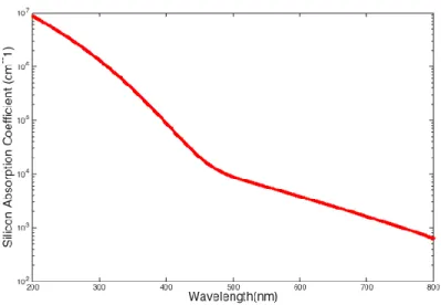
The absorption coefficient is a function of the wavelength and depends on semiconductor materials as well. For silicon, the relationship between the absorption coefficient and wavelengths is drawn in Figure 2-2.
Figure 2-2 Absorption coefficient vs wavelength in silicon.
2.2 Generation and Recombination
A photon with an energy, hv, which is larger than the band gap of silicon will excite an electron from the valence band to the conduction band and leave a hole in the valence band. This process is called generation. The typical band gap of silicon is 1.12eV, therefore, the minimum energy to generate electron-hole pair is 1.12eV, corresponding to the maximum photon wavelength of 1.1µm.
The recombination mechanism is the inverse process of the generation. When a free electron is captured by a positive ion, it combines with a hole. The SRH recombination mechanism is active where there are impurities or defects in the semiconductor material and the SRH lifetime is independent of excess carrier density. While Auger lifetime is independent of the impurity and defect densities, it is, however, a function of carrier concentration. In silicon, the Auger recombination mechanism dominates when either the doping density or the excess carrier concentration is very high, and the SRH recombination mechanism prevails at lower concentration [20].
2.3 CCD and CMOS Detector
Detectors are used to record the dispersed monochromatic beams and transform them into electrical signals. Two dominant optical sensor technologies are CCD (Charge-Coupled Device)
[6], [7] and APS (Active Pixel Sensor) [7]. There are several types of APS sensors, and the most widely used type in cell phone cameras, web cameras, and digital single-lens reflex cameras (DSLRs) is produced in CMOS (Complementary Metal-Oxide-Semiconductor) technology, hence, APS sensor is usually known as CMOS sensor.
CMOS image sensors appeared in the 1960s, earlier than CCD sensors. However, CCD sensors were dominant in this field until the 2000s, because of their lower noise, lower dark current, smaller pixel size, 100% fill factor, electronic shutter without artifacts and higher sensitivity [9]. Coming into the new millennium, thanks to the CMOS process state-of-art, CMOS image sensors attracted lots of attention for potentially higher performance than CCD sensors because they can offer many advantages compared to CCD sensors, such as faster response, lower cost, lower power consumption, lower operation voltage, on-chip functionality [9][10], and most importantly, the compatibility with mature CMOS technologies. This allows CMOS sensors to enter production during a very short period with high quality and low cost.
Both CCD and CMOS sensor have large detection bandwidth, covering the visible spectrum, therefore, they have no color selectivity. The color filters are employed on top of the sensor pixels to add color selectivity.
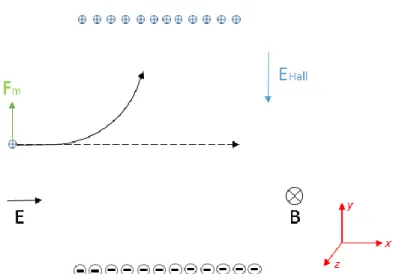
2.4 Hall Effect
As illustrated in Figure 2-3, a positive carrier q is moving under the electric field E with the velocity v in the +x direction as the dashed line showed. After applying an external uniform magnetic field B along –z direction, the carrier will deviate towards to the +y direction as the solid curve indicated under the Lorenz force, which is expressed as:
𝑭𝑚 = 𝑞𝒗 × 𝑩 (2.3) Thus positive carriers accumulate on top face in silicon and will leave equal negative carriers on the bottom face. The separated charges generate an electric field EHall along the –y direction. EHall can be derived when the total force applied on the carrier along the y direction equals to 0:
𝑭 = 𝑞[𝑬Hall+ 𝒗 × 𝑩] = 0 (2.4) 𝑬Hall= −𝒗 × 𝑩 (2.5)
2.5 State of the Art in Spectrometry
The electromagnetic spectrum, usually known as the spectrum, is a scientific collective term for all electromagnetic radiation’s frequencies and their linked wavelengths. It covers from gamma radiation to Extremely Low Frequency (ELF) region. Correspondingly, there are many types of spectrometry to measure different spectrum regions, such as X-ray Diffraction Crystallography, Ultraviolet-Visible Spectrometry, Fluorescence Spectrometry, Nuclear Magnetic Resonance (NMR) Spectrometry, Optical Spectrometry, Infrared Spectrometry, etc. [2], [4], [23].
The current research-grade optical spectrometers are bulky equipment composed of a light source, a dispersing element, lenses, an optical sensor, electromechanical components and electronic circuitry. The optical sensor and dispersing elements are the crucial components that determine the detection ability of a spectrometer.
The commonly used dispersing elements can be categorized into three main groups according to the mechanism involved in the extraction of spectral information from optical signals: spatial dispersion, interferometry, and resonance.
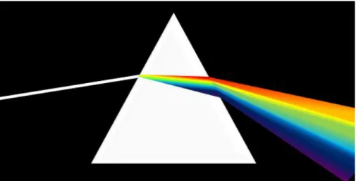
The spatial dispersing element mainly includes prism and diffraction grating. The dispersion of the prism is known since the 17th century, and the light obeys the Snell’s law at every optical surface. Figure 2-4 shows how a prism disperses an incident light.
Figure 2-4 Light is dispersed by a prism.
The diffraction grating consists of a series of parallel grooves used to separate the incident light into monochrome component wavelengths with different scattering angles. Figure 2-5 shows how a diffraction grating disperses an incident white light. The zero order (central white) represents a direct transmission through the grating. The first-order and second-order rainbows represent the increasing wavelengths from purple to red due to wavelength related diffraction angles. The diffraction order is determined by the grooves’ period, and adjacent order of rainbows may overlap, especially for higher orders. By adjusting the grooves’ density, it is possible to concentrate the diffracted energy in a particular order for a given range of wavelength.
Figure 2-5 Diagram of reflective diffraction grating principle [24].
The interferometer utilizes the interference phenomenon to disperse an incident light and the typical instruments are the Fabry–Pérot interferometer and the Michelson interferometer. They could record the frequency domain spectrum by Fourier transform, so both of them are also known as Fourier transform spectrometers.
As shown in Figure 2-6, a Michelson interferometer is composed of two mirrors M1, M2, a beam splitter M and a detector E. An incident beam produced by coherent light source is split at C by M and reflected by A and B, respectively, and both retuning beams are combined at C’ to generate an interference pattern due to the orientation of the mirrors, and the pattern is recorded by the detector E. The optical path difference caused by this process will result in interference. Figure 2-7 illustrates two possible interference fringes. M2’ is the image of mirror M2, S1’ and S2’ are virtual images of source S, respectively. The strictly perpendicular two mirrors M1 and M2 will make S1’ and S2’ are in line, and will generate fringes of equal inclination (Figure 2-7a), and a slight angle of two mirrors will result in fringes of equal thickness (Figure 2-7b).
Figure 2-6 Schematic diagram of Michelson interferometer principle [25].
Figure 2-7 Formation of fringes in a Michelson interferometer [26]. S1’ and S2’ represent the mirror images.
2.6 Recent development on filter-less optical sensor
Dispersing elements in a spectrometer are as crucial as color filter in a color sensor, and no one has ever tried to make a spectrometer without them. Giving that both spectrometer and color sensor are optical detection sensors, we present a short review on filter-less optical sensors.
Standard commercial cameras use the Bayer filter pattern [27] adding color sensitivity to CCD and CMOS sensors. However, filters reduce the pixel sensitivity due to the light reflection and scattering, and increase the production cost due to the post-processing filter deposition.
Recently, efforts to make filter-less image sensors have been made. Foveon Incorporated [17][28] has proposed a sensor structure in which three p-n junctions are implanted at different depths as shown in Figure 2-8. The first junction (upper) that is close to the surface collects the carriers generated by all photons in the visible spectrum. The middle junction collects mainly the carriers generated by all photons except the shorter wavelength (blue), and the deepest one collects mainly carriers generated by all photons except the blue and green range of the visible spectrum. The three junctions act as color filters. The latest product based on this detection principle from Foveon Incorporated is a 14.1 megapixels image sensor [29].
Figure 2-8Diagram of the Foveon sensor.
Another structure, called Transverse Field Detector (TFD), is proposed by Langfelder et al. in 2009 [30]. They implanted several independent N+ collectors in p-type silicon, applying selective voltages between them to generate an electric field in order to collect the carriers at different depths by different collectors. Figure 2-9 gives the simulation result of an electric field of the
TFD structure. The node n1 collects the carriers above depth X1 which generated by all photons in the visible spectrum, and n2 collects carriers coming from X1 to X2 range where carriers are generated except by blue ones, and n3 collects the all the carriers below depth X2. The three collectors act as color filters.
Figure 2-9 TFD simulation result. The streamlines show the electric field. The contact n1 collects the electrons to depth X1, contacts n2 collect electrons to depth X2, and collectors n3 collect other electrons
generated in other region. [30] [Year 2009 of original publication].
Maruyama et al. proposed filter-less fluorescence sensor in 2006 [31], and an improved sensor based on the same principle was reported in 2011 [32] by Nakazawa and in 2017 by Tanaka [33]. The structure and principle are given in Figure 2-10 and Figure 2-11, respectively. The voltage of the load transistor VLN is set at 0.5V and n-type substrate VSUB is biased at 5V. RES is the reset signal. The photogate PG has a voltage VG on it, and VG controls the depth where photo-generated carriers can be collected.
Figure 2-10 Schematic of sensor pixel and readout circuit [31]. Reprinted with permission from Elsevier.
Both VG and RES are set at 0V as in Figure 2-11(a), and RES is set at 5V to reset the floating diffusion (FD) output to 2.5V as shown in Figure 2-11(b). The similar readout operations are indicated in Figure 2-11(c) and (d) with different VG. VG in (d) is larger than in (c) to collect more electrons. The photon generated electrons are accumulated in FD well and the output signal is recorded in voltage after amplification. Because the excitation and fluorescent signals are simultaneous, the intensities could be solved with two VG values at least. Maruyama reported a linear relationship of incident intensity and detected intensity in a wide range of intensities for the fluorescence signal, while the excitation light remains unchanged. As illustrated in Figure 2-12, the author reproduced the excitation and fluorescent lights with 470nm and 530nm simultaneously, and kept the intensity of the excitation light constant, while varying it for 530nm. This relationship characterized the fluorescent wavelength.
Figure 2-12 Output of the filter-less fluorescence sensor [31]. Reprinted with permission from Elsevier. The sensor could detect the wavelength based on the linear ratio of fluorescence-to-excitation light since the wavelength and the intensity of the excitation light are already known.
2.7 Miniaturized spectrometer
The current research-grade spectrometer is bulky because it contains components and some space is necessary for an optical path. Some efforts have been made to miniaturized spectrometers and a handful of new products have emerged on the market to provide compact spectrometry solutions ([6], [34]–[43]) Traditional spatial dispersion elements, such as lens and gratings, are
still employed. However, exquisite optical path designs allow the spectroscopic systems to be accommodated in small containers.
2.8 Summary
Current spectrometers employ dispersing elements to discriminate the spectrum of an incident light. The widely used dispersing elements in optical spectrometer, including prism, grating, and interferometer are introduced. So far, no effort has been made to fabricate an optical spectrometer without dispersing elements.
Efforts made on the development of filter-less color sensor is a good starting point for the design of spectrometers without dispersing elements. The Foveon’s sensor and the TFD could detect three colors (red, green and blue.) It is a great result for color sensitivity but insufficient to distinguish the spectrum. Nakazawa’s design is able to detect up to three monochrome wavelengths simultaneously. However, it needs a calibration light signal every time which limits its applications.
At the same time, people have been working on miniaturization of a spectrometer. The efforts mainly focus on minimizing the volume of dispersing element and the optical path in order to reduce space requirement. One of the benefits of removing dispersing elements is that the required space is reduced so that more compact spectrometers can be fabricated
CHAPTER 3
A NOVEL CMOS SPECTROMETER BASED ON
WAVELENGTH ABSORPTIOION
3.1 Abstract
This article reports on a novel spectrometer without dispersing elements fabricated in standard CMOS technology. The spectrum detection principle is based on the wavelength absorption mechanism in silicon. A finite element model confirms the excess holes’ detection principle as a function of depth where moving holes’ trajectory is deviated under the Lorentz force towards a set of collectors. In the case of high excess carrier concentration, experimental results confirm the theoretical analysis that wavelength becomes indistinguishable because the Auger recombination mechanism is dominant, which should be avoided to realize a spectrometer. For the low excess carrier concentration case, the concentration profile is determined by the incident irradiance and the wavelength and can be additive since the Shockley-Reed-Hall recombination mechanism prevails, where the excess carrier life time is constant, and hence suitable for wavelength discrimination. In order to realize a spectrometer, a light spectrum detection method is developed, which requires a linear equation set where coefficients of the matrix coming from the measurement of the current density as a function of the irradiance for different wavelengths and magnetic fields. The proposed miniature and integrated spectrometer with a pixel array can be used as a spectral imager.
3.2 Introduction
Spectroscopy analysis is a powerful tool to investigate materials and structures. The current research-grade spectrometers are bulky equipment composed of a dispersing element, lenses, photo-detectors, electromechanical components and electronic circuits. The commonly used dispersing elements can be categorized into three main groups according to the mechanism involved in the extraction of spectral information from optical signals: spatial dispersion, interferometer, and resonance [1]. The latter group encompasses spectrometers using materials having properties of absorption, transmission, and reflection that are dependent on the wavelength. Recently a lot of interest has emerged in employing new structures and new
materials such as photonic crystals, metamaterials [44], [45] and quantum dots [1] as the detecting component of a spectrometer. In that respect, a color image sensors design to exploit the wavelength dependent absorption properties of silicon has been developed where the three primary colors employed in digital imaging, blue, green and red are extracted without thin film filtering. Recently, efforts have been made to miniaturized spectrometers and a handful of new products have emerged on the market to provide compact spectrometry solutions[34]–[37]. Traditional spatial dispersion elements, such as lens and gratings, are still employed. However, exquisite optical path designs allow the spectroscopic systems to be accommodated in small containers.
In this paper, we propose a new method of detecting the spectral content of luminous signals by exploiting the absorption properties of semiconductors. The method enables compact and cost effective spectrometer solution for a wide range of applications. Using silicon has the main advantage of having a detector compatible with some advance bipolar or CMOS integrated circuit fabrication processes, meaning that on the same substrate, the detector, signal conditioning circuits and digital processing can be implemented. The proposed principle employs the Lorentz force applied to moving charged particles in the presence of a magnetic field in order to relate wavelengths to the depth of photo-generated carriers. The paper is divided as follows: in Section 3.3, an overview of the underlying physics of carrier generation in semiconductor is described, followed by a description of the carrier concentration profiling method using the Lorentz force; in Section 3.4, a wavelength detection method is developed and also verified experimentally. It relies on a linear system of equations where the coefficients have been obtained from electrical measurement as a function of the optical irradiance for different wavelengths and magnetic fields. Finally, concluding remarks are presented.
3.3 Detection Principle
A monochrome light beam generates a unique excess carrier distribution along the incident depth due to the absorption coefficient. Hence, the wavelength information can be obtained by measuring the photo-generated carrier concentration as a function of depth, and the proposed spectrometer is named the Wavelength Absorption Spectrometer (WAS).
Figure 3-1 The schematic figure of the WAS prototype.
Figure 3-1 illustrates the schematic diagram of a WAS pixel. An N-well region is made in a P-type silicon substrate. Three P+ electrodes (red in Figure 3-1) are heavily doped regions and forms PN junctions with the N-well. The junctions are reversed biased to collect holes only. A uniform electric field along the +x direction is produced by the voltage difference between the two N+ contacts. Light penetrates into silicon through a window area and the oxide layer. Other regions are covered by metal to block the illumination. The light-generated electron-hole pairs are separated by the electric field, and electrons move along the -x direction and holes move along the +x direction. In this first WAS prototype, an external uniform magnetic field is applied along the -z direction, thus, the holes’ current flows towards the three P+ electrodes due to the Lorenz force. For a specific electric and magnetic field combination, the angle of deflection of holes’ current density is constant, so that the electrodes could collect holes from a specific depth. Holes are collected by the middle P+ electrode and form the hole current Im, while the left and the right P+ electrodes collect holes above and below that specific depth, and form current Is and Id, respectively. As a result, excess holes’ concentration profile along the depth (-y direction) could be achieved by varying the magnetic field, hence, the current density angle of deflection.
In the theoretical analysis, we firstly derive the equation giving the photo-generated excess holes’ concentration distribution along the –y direction, and secondly, the excess holes’ transportation mechanism from the window area to the P+ collectors is validated with a finite element model implemented in the software tool COMSOLTM [46] and experimental result.
3.3.1 The excess holes’ generation and recombination
The steady-state continuity equation describes the carrier behavior under the constant incident illumination [47]. Considering the holes’ concentration variation along the depth under the window area, the equation becomes
D𝑝
d2δ𝑝(|y|)
dy2 −
δ𝑝(|y|)
τ𝑝 + g𝑝 = 0 (3.1)
where δ𝑃 is the excess holes’ concentration, D𝑝, the diffusion coefficient [48], and, |𝑦|, the depth from the surface (y=0). For an illumination irradiance, P, at a specific wavelength, λ, the generation rate, g𝑝, is defined as [20]
g𝑝 = P𝜆
ℎ𝑐αλ(1 − Re)e
−αλ|𝑦| (3.2)
where αλ is the absorption coefficient, Re is the reflectivity at the Si/SiO2 interface, h is Plank constant, and c is the speed of light.
The hole recombination lifetime, τ𝑃, is not constant and is determined by the Auger and the Shockley-Read-Hall (SRH) recombination mechanisms
1/τ𝑝 = 1/τAuger+ 1/τSRH . (3.3)
The SRH recombination mechanism is active where there are impurities or defects in the semiconductor material while Auger lifetime is independent of the impurity and defect densities.
In silicon, the Auger recombination mechanism dominates when either the doping density or the excess carrier concentration is very high, and the SRH recombination mechanism prevails at lower concentration [20]. Auger lifetime is a function of carrier concentration, while SRH lifetime is independent of excess carrier density.
At high concentration in N-type silicon as in the scenario of Figure 3-1, the Auger recombination mechanism dominates and the hole lifetime becomes
τ𝑝= τAuger= 1/[C𝑛(𝑛02+ 2𝑛
0𝛿𝑃 + 𝛿𝑃2) + C𝑝(𝑝02+ 2𝑝0𝛿𝑃 + 𝛿𝑃2)] (3.4) where Cp and Cn are the Auger recombination coefficients for holes and electrons respectively
[11]. For holes’ excess concentration 𝛿𝑃 of 1020 cm-3, which is much larger than the equilibrium concentration of electrons, 𝑛0, and holes, 𝑝0, Equation (3.4) becomes
τ𝑝 = τAuger = 1/[𝛿𝑃2(C
𝑛+ C𝑝)] (3.5)
and the lifetime decreases rapidly to reach approximately 1 ns [20]. In these conditions, the recombination term in Equation (3.1) is dominant and the continuity equation becomes
D𝑝d 2δ 𝑝(|y|) dy2 − δ𝑝(|y|) τ𝑝 = 0. (3.6)
Consider the boundary conditions δ𝑝(0) = g𝑝(0), where δ𝑝(0) is the surface excess hole density and δ𝑝(∞) = 0, the analytical solution of Equation 3-6 is:
1 δ𝑝(y)= |𝑦| √2D𝑝⁄(C𝑛+C𝑝) + ℎ𝑐 P𝜆αλ(1−Re) . (3.7)
and reveals that the slope of the reciprocal of photo-generated holes’ concentration versus depth is wavelength-independent at high carrier concentration condition. A high incident illumination
induces a high carrier concentration, and Equation (3.7) indicates that high illumination must be avoided for the spectrometer application.
At lower photo-generated carrier concentrations, for example, when the concentration can be compared to the equilibrium concentration, both Auger and SRH recombination mechanisms play roles, and g𝑝 can’t be ignored in Equation (3.1). g𝑝 is wavelength-dependent, therefore, the carrier concentration distribution along depth provide the spectrum information of the incident light. However, given the relationship of 𝜏𝑃 and g𝑝, Equation (3.1) is a linear non-homogenous differential equation that doesn’t have an analytical solution. The effort to reveal the relationship of carrier concentration vs. depth by experiments is reported in Part 3.3.3.
3.3.2 The excess holes’ transportation under magnetic field
Analysis of the holes’ current density traveling from the volume under the window area up to the collectors and submitted to perpendicular electric and magnetic fields requires coupled equations involving drift and diffusion current densities. Adding to that the geometrical effect of adjacent collectors, makes the derivation of an analytical solution extremely complicated and most likely not representative of the structure. Instead, a Finite Element Method (FEM) model implemented with the multi-physics software tool COMSOLTM is employed to validate the holes’ transportation.
Excess electrons and holes are separated and form current densities under the electric and magnetic field. The hole’s current density obeys the equation [49]
𝑱𝑝 (𝑩) = 𝑱𝑝 (0) + 𝜇𝑃(𝑱𝒑 (𝑩) × 𝑩) (3.8)
where 𝑱𝑝 (0) is the hole current density without magnetic field, B, and it includes drift and diffusion components. Drift current density is a function of electric field and is expressed as 𝐽𝑝_𝑑𝑟𝑖𝑓𝑡 (0) = 𝑞𝜇𝑃𝛿𝑃𝐸𝑥, where q is the elementary charge. Diffusion current density is mainly due to the concentration difference between the illuminated and the shaded area in the substrate.
From the diffusion equation [47], the average diffusion current density is 𝐽𝑝_𝑑𝑖𝑓𝑓 (0) = 𝑞𝐷𝑝𝛿𝑃(1 − 𝑒−𝐿 𝐿⁄ 𝑝)/𝐿 where L
p is the hole diffusion length which is related to the lifetime and L
is the horizontal distance from the middle-point of the window area to the middle P+ collector, as shown in Figure 3-2 (a). Calculation shows that the drift current density is about three orders of magnitude larger than the diffusion, therefore, the diffusion current density component is negligible and hole concentration is mainly determined by drift.
In the scenario of Figure 3-1, 𝑱𝑝 (𝑩) has x and y components while 𝑱𝑝 (0) has only a component along x and B exists along z, Bz. Thus,
𝐽𝑝 (0) = 𝑞𝜇𝑃𝛿𝑃𝐸𝑥+ 𝑞𝐷𝑝𝛿𝑃 𝐿 (1 − 𝑒 −𝐿 𝐿⁄ 𝑝) ≅ 𝑞𝜇 𝑃𝛿𝑃𝐸𝑥, (3.9) 𝐽𝑝𝑥 (𝐵) = 𝐽𝑝 (0) − 𝜇𝑃𝐽𝑝𝑦 (𝐵)𝐵𝑧, (3.10) 𝐽𝑝𝑦 (𝐵) = 𝜇𝑃𝐽𝑝𝑥 (𝐵)𝐵𝑧 = 𝜎𝑝𝐸𝑦 = 𝑞𝜇𝑃𝛿𝑃𝐸𝑦, (3.11) 𝑡𝑎𝑛𝜃 = 𝐽𝑝𝑦 (𝐵) 𝐽𝑝𝑥 (𝐵)= 𝜇𝑝𝐵 (3.12)
where, 𝐸𝑦 is the Hall electric field, 𝜃 is the Hall angle. Since there is no electron current density in y direction at equilibrium,
𝐽𝑛𝑦 (𝐵) = 𝑞𝜇𝑛(𝐸𝑦− 𝜇𝑛𝐵𝑧𝐸𝑥) = 0, (3.13)
and combining Equations (3.9) to (3.11), the excess hole concentration 𝛿𝑃 is obtained
𝛿𝑃 = 𝐽𝑝𝑦 (𝐵) (𝑞𝜇𝑝2𝐵𝐸 − (𝜇𝑝𝐵) 3
𝑞𝜇𝑛𝐸)
⁄ (3.14)
where 𝐽𝑝𝑦 (𝐵) can be deduced by measuring the current, Im, of the middle collector .
Figure 3-2 shows the simulated holes’ concentration profile and holes’ current density in a pixel of WAS under electric field and a magnetic field varying from 0T to 3T. The magnetic field is pointing inward in a direction perpendicular to the paper. As shown in Figure 3-2, the middle P+
collector collects holes coming from a certain depth in the window area. At B=0T in (a), the current density presented by black lines is parallel to the surface in the window area and then slightly bends when reaching the collectors’ region. While increasing the magnetic field, holes move up under the Lorenz force, and the Hall angle increases, allowing the collection of holes generated deeper in the N-well, as shown by the current density lines in (b), (c) and (d) for 1, 2 and 3 T respectively. Hence, by sweeping the magnetic field, it is possible to measure the excess holes’ concentration along the depth.
Figure 3-2 (a)
Figure 3-2 (c)
Figure 3-2 (d) Figure 3-2 COMSOLTM modeled results of a pixel at magnetic flux density, B= (a) 0T, (b) 1T, (c) 2T, and
(d) 3T. The red area represents the high concentration region, and the low concentration region is in blue. The black lines illustrate the electric field orientation, and the blue lines represent the electric potential.
3.3.3 Experiment details and data analysis
In this section, important experiment details including the pixel array architecture of the WAS are presented, and experimental results validate the behavior of the proposed sensor.
As illustrated in Figure 3-3, the WAS is composed of an array of 20x20 pixels along with pass transistors in order to direct the collected currents row-wise and column-wise down to three common outputs to each Is, Im and Id pixel collector. Benefits of disposing of the proposed spectrometer in an array include the increase of the dynamic range and the capability of using the array as a micro spectral imaging sensor.
Each pixel is composed of three NMOS transistors, as shown in the red circle. They link the collectors to the vertical buses, t when the row selector signals, R0 to R19, are applied to their gates. The logic inverter allows the use of the same signal to establish an electric field in the pixel, and activate the row selection transistors. When R0 is set to 0V and other rows are 5V, an electric field is generated in the pixels of the first row, oriented towards the N+ contact of the row R0. The NMOS transistors on the row are turned ON through a logic inverter, such as only pixels in the row ‘0’ are activated. In addition, column selector transistors are selected by the column control signal to connect one pixel at a time to the output bus. To allow the measurement of small currents and reduce the noise bandwidth, each line of the output bus is connected to an off-chip integrating transimpedance amplifier, as shown in Figure 3-4.
Figure 3-5 shows the printed circuit board, on which the pixel array is bounded. The pixel array is fabricated in 0.5 μm CMOS technology. It is placed at the center between two electromagnetic poles, as shown in Figure 3-6. The control board contains all the components of the reading circuit. It is connected to the sensor board by a flexible flat cable. To eliminate the mechanical forces acting on the pixel array and thus to avoid disturbing the optical alignment, all the conductors are made of copper only, which is a diamagnetic material.
Figure 3-4 Schematic figure of an integrating transimpedance amplifier. The switch S is used to reset the capacitor after a pre-determine integration time.
Figure 3-6 Experimental setup uses to test the WAS prototype.
The spectrometer is placed in an adjustable electromagnetic field and is illuminated by a light source at different irradiances and wavelength. The intensity of the magnetic field between the two poles depends strongly on the distance between them and the diameter of their external faces. The objective is, therefore, to have the part of the sensor board hosting the chip as slim as possible in order to obtain a wide range of magnetic field values between the two poles.
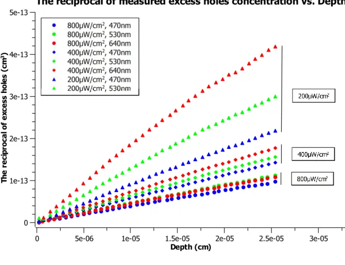
Figure 3-7 gives the experimental relationship of the reciprocal of detected excess holes’ concentration versus depth. The concentration 𝛿𝑃 is derived from 𝐽𝑝𝑦 (𝐵) = 𝑉𝐶/𝑡𝐴 and Equation 3-14, 𝛿𝑃 = 𝑉𝐶/[𝑡𝐴 (𝑞𝜇𝑝2𝐵𝐸 +𝑞𝐷𝑝 𝐿 (1 − 𝑒 −𝐿 𝐿⁄ 𝑝)𝜇 𝑝𝐵 − (𝜇𝑝𝐵) 3 𝑞𝜇𝑛𝐸)] (3.15)
where C is the capacitor (10pF) of the integrating transimpedance amplifier as seen in Figure 3-4,
t is the integration time, A is the surface area of a P+ collector, and V is the amplifier output
data processing in order to remove the effect of the dark current on the P+ collector. The depth value |𝑦| as introduced in Equation 1 is derived based on the Hall Angle 𝜃 which is function of the magnetic field Bz,
|𝑦| = 𝐿 𝑡𝑎𝑛𝜃 (3.16) Figure 3-7, chromatic illumination results at 470 𝑛m, 530 𝑛m, and 640 𝑛m, are represented in blue, green and red, respectively. The chromatic illuminations have been obtained from a halogen lamp with 70 nm bandwidth color filters. Excess holes’ concentration is calculated according to Equation (3.15) from the measured voltages under three incident illumination irradiances (200W/cm2, 400W/cm2, and 800W/cm2). As seen on the graph, as the irradiance increases, the 1/𝛿𝑃vs |y| relationships becomes more linear with slope values converging toward a constant as predicted by Equation (3.7) at high excess holes’ concentrations where the Auger
recombination mechanism is dominant. For each irradiance, the concentration generated by the 470 nm wavelength photons exhibits higher values due to the fact that penetration depth decreases for high energy (shorter wavelength) photons. That trend is also confirmed by
concentrations produced by green photons (530 nm) being larger than the one of the red photons (640 nm).
Figure 3-7 The reciprocal of detected excess holes concentration variation obtained by sweeping the magnetic field for several illumination irradiances.
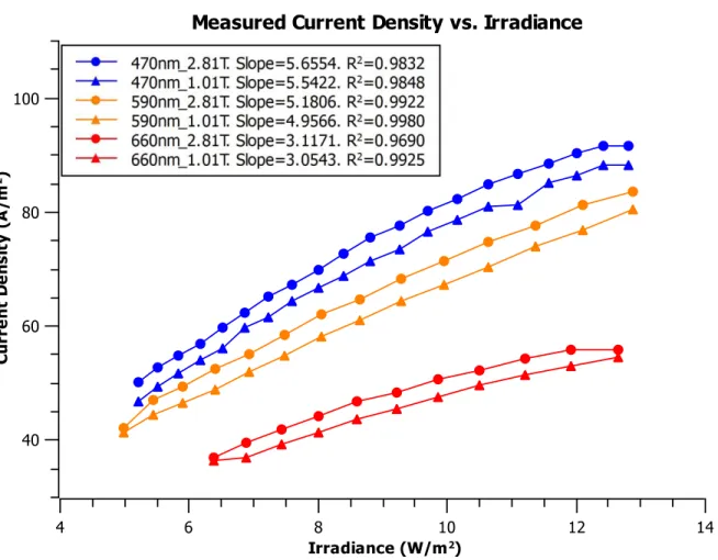
3.4 Application as a spectrometer
In order to use the WAS as a spectrometer, the substrate must be in the SRH recombination regime where it is independent of the excess carrier concentration. We assume that photo-generated holes coming from different wavelength are additive, hence a linear system of equation can relate the irradiance of the light signal spread over a given spectrum to the collector currents. Through a calibration procedure, a system of linear equation can be built. Figure 3-8 illustrates the experimental curves of current density of the middle P+ collector as a function of the irradiance for three wavelengths, 𝜆=470 𝑛m , 590 𝑛m and 660 𝑛m, for two constant magnetic fields, 2.8 T and 1.0 T. The graph depicts quasi-linear relationships of current densities as a function of irradiances.
Figure 3-8 Measured current density as a quasi-linear function of the irradiance of 470 𝑛m (blue), 590 𝑛m (orange) and 660 𝑛m (red), at B=2.81T (round) and 1.01T (triangle).
For an illumination composed of n discrete wavelengths, the current density J, can be expressed as
𝐽 = 𝑚𝜆1𝐼𝜆1+ 𝑚𝜆2𝐼𝜆2+ ⋯ 𝑚𝜆𝑛𝐼𝜆𝑛+ 𝑛𝐽0 (3.17)
where terms 𝐼𝜆𝑥 are the irradiance of the wavelength, 𝜆𝑥, 𝑚𝜆𝑥 are the slopes of the current density versus irradiance relationship for 𝜆𝑥 and J0 is the current density collected in the dark. Equation
(3.17) represents a linear equation with n unknown 𝐼𝜆𝑥. Terms, 𝑚𝜆𝑥 have been measured previously from n chromatic filters having non-overlapping band pass and a center wavelength,
𝜆𝑥. In order to solve Equation (3.17), we need a set of n equations. Given that the slopes of the J
vs 𝐼𝜆𝑥 relationships vary not only with respect to the wavelength but also with respect to the magnetic field, it is then possible to obtain the following solvable system of equations,
𝐽𝐵1 = 𝑚𝐵1,𝜆1𝐼𝜆1+ 𝑚𝐵1,𝜆2𝐼𝜆2+ ⋯ 𝑚𝐵1,𝜆𝑛𝐼𝜆𝑛+ 𝑛𝐽𝐵1,0
𝐽𝐵2 = 𝑚𝐵2,𝜆1𝐼𝜆1+ 𝑚𝐵2,𝜆2𝐼𝜆2+ ⋯ 𝑚𝐵2,𝜆𝑛𝐼𝜆𝑛+ 𝑛𝐽𝐵2,0 (3.18) ⋯
𝐽𝐵𝑛 = 𝑚𝐵𝑛,𝜆1𝐼𝜆1+ 𝑚𝐵𝑛,𝜆2𝐼𝜆2+ ⋯ 𝑚𝐵𝑛,𝜆𝑛𝐼𝜆𝑛+ 𝑛𝐽𝐵𝑛,0
where the suffix Bx indicates different magnetic field values. Hence, Equation
(
3.
18) can be written in a matrix form,𝐽𝐵 = 𝑀𝐵𝜆𝐼𝜆+ 𝐽𝐵,0 (3.19)
where JB and JB,0 are the n×1 vector representing the measured current densities with and without
illumination respectively, 𝑀𝐵𝜆 is the n×n matrix of the JBx vs 𝐼𝜆𝑥 slopes and 𝐼𝜆 is the n×1 vector
of the irradiances. Therefore, the solution can be found from
𝐼𝜆 = (𝐽𝐵− 𝐽𝐵,0)𝑀𝐵𝜆−1. (3.20)
Coefficients of matrix 𝑀𝐵𝜆 are obtained from the slopes of calibration curves as the ones shown in Figure 3-8.
3.5 Conclusion
A novel spectrum detection method is proposed, and the mechanism is discussed in this article. The detection principle is based on the wavelength absorption in silicon where the photon-generated excess holes’ concentration is a function of depth, wavelength, and irradiance. Variable magnetic field enables the measurement of the excess carrier concentration profile as a function of depth. Experimental results of collected current densities as a function of irradiances for different magnetic fields have validated the detection principle that relies on the additive property of photo-generated carriers when the device is in the SRH recombination regime. Those quasi-linear relationships are employed to determine the coefficients of a matrix used to solve
algebraically a set of linear equations linking the measured current densities to the wavelength spectrum of the incident light. The small footprint of the WAS and its compatibility with standard CMOS fabrication processes allow for the design of an array which enables applications in the field of spectral imaging. Future work will be focusing on improving the current density vs. magnetic field linearity on a wider dynamic range by modifying the pixel geometry and implementing the WAS in smaller feature size CMOS processes.
CHAPTER 4
RESOLUTION ANALYSIS
4.1 Definition of Resolution
The resolution is a crucial parameter for a spectrometer. It is necessary to calculate the resolution of the WAS to understand its ability, limitation, and the ways to improve it. No magnetic field is considered to simplify the analysis.
The spectrometer resolution is defined as: R = λ
∆λ (4.1) where ∆λ is called the resolving power, which is the minimal wavelength difference that can be distinguished.
4.2 The resolution of the WAS
The WAS doesn’t detect the wavelength directly, instead, it detects the hole current. Thus, its resolving power is limited by the minimum detectable current. The ∆δ is defined as the minimal detected carrier concentration variation, which is determined by the shot noise [50]:
𝑖𝑛2 = 2𝑞𝐼𝐷𝐶∆𝑓 (4.2) ∆𝛿 = √𝑖𝑛2⁄(𝑞) (4.3)
𝐼𝐷𝐶 is the detected current, the experimental value is approximately 10-12A. ∆𝑓, 10 MHz, is the
bandwidth of the oscilloscope employed to measure the current for the prototype WAS. The black line in Figure 4-1 represents the ∆δ.
For the WAS prototype, without the magnetic field, the difference in excess holes’ concentration of two wavelengths is expressed as:
∆𝛿′= |∫ 𝛼1I1e−𝛼1ydy y2 y1 − ∫ 𝛼2I2e −𝛼2ydy y2 y1 | (4.4)
where y1 and y2 are the vertical boundaries of the region where the carriers are collected. As
shown in Figure 4-1
,
∆𝛿′ is calculated for various wavelengths, 450 𝑛m (blue curve), 550 𝑛m (green curve), 650 𝑛m (cyan curve), and 750 𝑛m (red curve), respectively.Figure 4-1 The calculated resolving power vs. wavelength by MATLAB, at the same incident power. The red curve and the cyan curve are almost coincident.
When ∆𝛿 = ∆𝛿′, the abscissa of the intersection is the resolving power. In Figure 4-1, the resolving power is within a range of 3 𝑛m to 19 𝑛m over the range (450 𝑛m to 750 𝑛m).
Figure 4-2 The calculated resolution vs wavelength at the same incident power.
Figure 4-2 gives the resolution of the WAS over the range 400 𝑛m to 800 𝑛m. The best resolution reaches 219 at the 438 𝑛m, and the smallest resolution is around 10 at 475 𝑛m. The non-linear resolution-wavelength relationship indicates that the resolution of the WAS is determined by mainly two factors: the absorption coefficient and geometry. The 400 𝑛m to 800 𝑛m range is divided into four zones, and the resolution in each zone will be discussed, respectively. Zone 1: 400 𝑛m to 438 𝑛m; Zone 2: 438 𝑛m to 475 𝑛m; Zone 3: 475 𝑛m to 525 𝑛m; Zone 4: 525 𝑛m to 800 𝑛m. As shown in Figure 4-2.
Zone 1 & 2: From Figure 2-2, it is clear that, wavelengths in Zone 1 and Zone 2 have much higher absorption coefficient and therefore generates carriers closer to the surface which form a larger current Im. In addition, this range has a big slope 𝑑𝛼⁄𝑑𝜆 , which induces a bigger difference of carrier concentration generated by the adjacent wavelengths and explains the higher resolution. Wavelength (nm) 400 450 500 550 600 650 700 750 800 R e sol u ti on 0 50 100 150 200 250 Resolution vs. Wavelength
2 3
4
1
Zone 1: For the reasons stated above, should have higher resolution than Zone 2. However, the resolution drops with the wavelength becoming shorter. This is the same effect as observed in Figure 4-3 where carriers closer to the surface are collected by the left P+ electrode and have less contribution to the current Im.
Figure 4-3 The three P+ electrodes collect holes coming from different depths.
Figure 4-4 Photo-Generated hole carrier concentration along the depth. The dash lines show the boundaries of the holes concentration integration.
Zone 4: As seen in Figure 2-2, the 475 𝑛m is an inflection point, after which the 𝑑𝛼⁄𝑑𝜆 becomes smaller. This will decrease the resolution, as shown in Figure 4-2. In this region, the resolution is in the vicinity of 30 for a maximum of 50.
Zone 3: This is a special range because the absorption coefficient is still high but the resolution is very low. The Equation 4-4 indicates that the low resolution is determined by the small difference of the generated carrier concentration. Actually, the concentration is an integration result between 0.8 𝜇m and 1 𝜇m, not from a single depth, as shown in the Figure 4-4. The integration range is limited by the designed geometry, as shown in Figure 4-3. A different geometry will bring a different integration range. Figure 4-4 gives the concentration variation with the depth for several wavelengths (from 475 𝑛m to 525 𝑛m). It is clear that the integration results of these wavelengths are similar due to actual position of the depth integration limits (from 0.8 𝜇m to 1 𝜇m). It explains why the WAS prototype has smallest resolution in Zone 3.
For the current WAS prototype, the best theoretical resolution occurs in Zones 1 and 2. The Zone 4 has a stable resolution, and Zone 3 should be avoided for high accuracy application.
To expand the best detection spectrum region, the geometry and structure modification is necessary. The possible improvements may include: a smaller depth for the left P+ electrode, more P+ electrodes, and a larger distance between the electrodes.
4.3 Conclusion
The study on resolution of the Wavelength Absorption Spectrometer (WAS) based on experimental data and a finite element model proved its functionality. The theoretical calculation predicts that the resolution of the WAS could reach around 219 depending on the collectors’ junction shot noise. The structure requires further development for better performance.
CHAPTER 5
SOLUTION OF CONTINUITY EQUATION
In previous chapters, we analyzed the photo-generated excess carriers’ generation, recombination and transportation under an electric and magnetic field. In this chapter, we pay attention to the effect of some parameters of the continuity equation in order to get a full view of the mechanisms of generation and recombination. All discussions are related to the one dimensional photo-generated excess holes without electrical and magnetic field.
The photo-generated excess holes’ concentration is described by the continuity equation. D𝑝
d2δ𝑝(|y|)
dy2 −
δ𝑝(|y|)
τ𝑝 + g𝑝 = 0 (5.1)
Where τ𝑝is the holes’ lifetime, δ𝑃 is the excess holes’ concentration, D𝑝, the diffusion coefficient [48], and, |𝑦|, the depth from the surface (y=0). For an illumination irradiance, P, at a specific wavelength, λ, the generation rate, g𝑝, is defined as [20]
g𝑝 = P𝜆
ℎ𝑐αλ(1 − Re)e
−αλ|𝑦| (5.2)
where αλ is the absorption coefficient and Re is the reflectivity at the Si/SiO2 interface.
5.1 Boundary conditions
Different boundary conditions result in different solutions to Equation (5.1). For the WAS prototype, there are four possible boundary conditions. All of them are discussed in this chapter.
Photons generate excess carriers in N-well and P-substrate regions. However, only the N-well region is of interest since the collected holes come mainly from the N-well. The reversed-biased PN junction prevents the abundant holes in the P-substrate to be collected.
![Figure 2-7 Formation of fringes in a Michelson interferometer [26]. S 1 ’ and S 2 ’ represent the mirror images](https://thumb-eu.123doks.com/thumbv2/123doknet/2352629.36616/26.918.283.638.564.890/figure-formation-fringes-michelson-interferometer-represent-mirror-images.webp)
![Figure 2-11 Operation of the filter-less fluorescence sensor [31]. Reprinted with permission from Elsevier](https://thumb-eu.123doks.com/thumbv2/123doknet/2352629.36616/29.918.148.767.599.967/figure-operation-filter-fluorescence-sensor-reprinted-permission-elsevier.webp)