HAL Id: dumas-00636795
https://dumas.ccsd.cnrs.fr/dumas-00636795
Submitted on 28 Oct 2011HAL is a multi-disciplinary open access archive for the deposit and dissemination of sci-entific research documents, whether they are pub-lished or not. The documents may come from teaching and research institutions in France or
L’archive ouverte pluridisciplinaire HAL, est destinée au dépôt et à la diffusion de documents scientifiques de niveau recherche, publiés ou non, émanant des établissements d’enseignement et de recherche français ou étrangers, des laboratoires
Design and study of a massively multi threaded shared
memory architecture
Christophe Riolo
To cite this version:
Christophe Riolo. Design and study of a massively multi threaded shared memory architecture. Distributed, Parallel, and Cluster Computing [cs.DC]. 2011. �dumas-00636795�
Design and study of a massively multi threaded
shared memory architecture
Internship report Research master’s degree in computer science Universit´e de Rennes 1
Author : Christophe Riolo Supervised by Dominique Lavenier Symbiose team, IRISA June 2nd, 2011
Abstract
Most biocomputing problems require a high processing power with high memory needs while showing massive paral-lelism opportunities. Unfortunately, although advances are made in software parallelism, current architectures do not provide a transparent way to use this parallelism at its full potential. We thus started to design an massively parallel megathreaded architecture that would match biocomputing algorithms requirements both in terms of processing power and memory.
Contents
1 Introduction 5
2 State of the art 6
2.1 Massively Parallel Processor Arrays . . . 7
2.2 General Purpose GPUs . . . 9
2.3 MIMD architectures . . . 13
2.4 Conclusion . . . 13
3 The massively multi threaded shared memory architecture 15 3.1 Motivations and objectives . . . 15
3.2 Multithreaded processor . . . 16
3.3 The network. . . 17
3.3.1 Direct implementation of a multistage network . . . . 17
3.3.2 Second architecture: a step further from theory . . . . 21
4 Experimental results 22 4.1 Experimental setup. . . 22
4.2 First architecture . . . 24
4.2.1 Components parameters . . . 24
4.2.2 Results and analysis . . . 24
4.2.3 Protocol presentation . . . 25
4.3 Prospective results of the second architecture . . . 27
5 Conclusion 27 A Three dimensional conception 31 B Protocol for each component 33 B.1 Messages . . . 33 B.2 Channels . . . 34 B.3 Switches . . . 34 B.3.1 Normal routing . . . 34 B.3.2 Multicast . . . 34 B.3.3 Conflicting transmission . . . 35 B.3.4 Pseudo-code protocol . . . 36 C Example of transmission 38 D Example of architecture description 39 E Statistics 39 E.1 Some statistics for 5000 cycles, with 2048 memories and 1024 processors . . . 39
E.1.1 Simple processor (random instructions) . . . 40
List of Figures
1 The Am2045 chip . . . 8
2 Am2045 tile architecture . . . 8
3 Interconnection of neighbouring tiles . . . 9
4 Comparison of CPU and GPU . . . 10
5 GPU architecture detail . . . 11
6 Thread block and grid hierarchy . . . 12
7 MIMD classification . . . 14
8 Theoretical best architecture . . . 15
9 Communication through a network . . . 16
10 Latency and multithreading . . . 17
11 Processor description . . . 18
12 Bus hierarchy . . . 19
13 Baseline network . . . 20
14 Multi layered technology . . . 21
15 Two dimensional architecture . . . 22
16 Simulator description. . . 23
17 Comparison of simple and SPMD processors . . . 26
18 Blender representation of a baseline network. . . 31
19 Baseline network on multiple cards . . . 32
20 A switch is mainly a router from two inputs to two outputs. In our architecture, the four channels are bidirectional. . . 33
21 Routing of a single message . . . 35
22 Conflict-free transmission of messages . . . 36
23 Multicast massages . . . 36
24 Message transmission. . . 38
List of Tables
1 Comparison of different architectures . . . 6Acknowledgements
I would like to thank all the people who supported me during this internship, with special mention to all members of the Symbiose team.
Special thanks to Dominique Lavenier for his supervision and for having given me the opportunity to do this internship.
Special thanks also to the other interns at Symbiose, especially but not restricted to Mathilde, Gaelle and Sylvain, for their support and for the lively — yet serious — atmosphere.
Special thanks again to Eily and neko for their advice and corrections. Thanks also to other people who supported me and will recognize them-selves.
1
Introduction
Biological data require a tremendous computing power to be processed. Not only do the databases grow exponentially but the algorithms used require a lot of computation and of memory.
Let us consider the well publicized example of human DNA alignment. First, fragments of a person’s genome, reads, are now obtained via next generation sequencing techniques, for instance Illumina sequencing. One run of Illumina sequencing produces approximately 50 million reads. We often perform multiple runs, so we can reach a billion of 40 base pair1 reads to be aligned to a 3 billion base pairs reference genome. A very demanding computation indeed.
Next generation sequencing (NGS)[Mar08,Ans09] has definitely brought genome analysis into the new century. Previously, extracting sequences of a genome was a highly time consuming task, since hundreds of thousands sequences had to be extracted by groups of only a hundred. Now, millions of sequences are extracted in a massively parallel way. This high throughput technique has made possible the study of new fields of genomics but also raised new challenges. Not only are the sequences of lower quality, since smaller ; this massive library of sequences created during the sequencing need be processed. Fortunately, this data obtained with massive parallelism can also be treated with massive parallelism. The data produced is made of sequences that can all be treated independently from one another. It would be possible to define a GPU-like routine executing multiple instances of the same code to process all sequences in parallel, provided an architecture can execute it.
This example is quite representative of biocomputing. Considering DNA analysis only, we have over a thousand human genomes, and numerous other species too. Then we can consider other problems, more complex, manipu-lating complex structures, sometimes NP-complete, and we have a glimpse of the complexity of biology and bioinformatics. To address this problem, different kind of architectures are currently used. The first is a server, pro-viding a lot of memory and a powerful core, but little parallelism. To achieve more parallelism, the clusters provide numerous cores, but the data has to be correctly distributed on the nodes. A third architecture that provides massive parallelism is GPUs2, which have long been used for general pur-pose computing. GPUs have many processing units, more than clusters, but their programming model is limited and they have less memory. This is summarized in table1.
Still all architectures show disadvantages. For instance, the server does not have enough cores, the cluster needs further adaptation of the software
1
A base pair is roughly a nucleotide, that is to say one of the letters A,C,G or T.
Architecture Nb cores Memory type Memory size Parallelism type Server ˜8 centralized 512 Go to 1 To mainly SPMD
Cluster 10 to 100 distributed several To any
TESLA 448 split / local 6Go SIMD
Table 1: Comparison of different architectures that can be used in bioinformatics. The GPUs evolve quickly so we chose a Tesla C2070 card. Each architecture has its advantages and disadvantages. The server has little processing power compared to the others. The cluster has more processing power but the data has to be distributed on the different nodes, and not all softwares can be scaled to run on a cluster. The graphic card has many processing units, but has little memory, and its management is complicated for the developer.
that is not always possible, the GPU does not have enough memory. There-fore we started to develop a new architecture that would be able to answer the needs of bioinformatics algorithms. We sought inspiration in diverse existing massively parallel architectures, some modern some not, to design an architecture able to run a massive load of similar threads sharing a great memory. We thus designed two different architectures where numerous pro-cessors are connected to not less numerous memories, running hundreds of threads to hide the memory access time so that the threads are not slowed down.
We will first present a short state of the art of massively parallel architec-tures from which we got inspiration, more precisely three different general purpose architectures. Then we will explain the general design of our archi-tecture an show how its originality resides in the massive multithreading, before detailing the two designs tested. Then, we will analyse the experi-mental results to show the pros and cons, and finally we will conclude with a summary and perspectives.
2
State of the art
For years, processor evolution has been dictated by Moore’s Law, stating that the number of transistors on a single chip doubles every 18 months. Since 2005, this evolution is no longer possible since miniaturization is reach-ing its limits due to several factors includreach-ing heat dissipation. Concurrently — no pun intended —, at the program level, parallel programming has be-come more and more widely used to improve program efficiency, especially since the high performance architectures gave birth to power hungry pro-grams, e.g. in scientific computation.
In this context arose the need for parallel architectures. The supercom-puters once monolithic have been replaced by clusters and clouds of clus-ters. The processors have been replaced first by multi-processor and then by multi-core processors, and according to some authors ([FB09]) Moore’s law
is now about doubling the number of cores instead of transistors. Intel has recently revealed its Knights corner project that would implement around 50 cores [intb], and another project that aims to implement cloud computing on a single chip [inta] mimicking the highly popular distributed computing paradigm.
But this might not be sufficient, some applications being highly demand-ing in parallelism[Gue10]. To address this issue, two kind of massively par-allel architectures coexist: general purpose architectures and architectures dedicated to a single activity. Although our goal is to develop a general purpose architecture, we sought inspiration in both general purpose and specific architectures. We will focus on three general purpose architectures: massively parallel processor arrays, GPUs and MIMD architectures. We will notably explain the choices made concerning access to memory and the programming model. We will conclude this state of the art by explaining why those architectures may still not be sufficient.
2.1 Massively Parallel Processor Arrays
Massively parallel processor arrays are, as their name suggest, a tiling of a great number of processors. Although they are designed mainly for stream-ing media, they can be used for various applications. We will here study the Am2045, an MPPA designed by the company Ambric[But07a, Hal06,
But07b].
Am2045 architecture The Am2045 is an array of 9 × 5 tiles contain-ing each 8 processors. The tiles are composed of two compute units and two memory units (fig. 1). After those raw facts, let us describe more pre-cisely the architecture of a tile and the core of the card, the communication between tiles.
The architecture of half a tile can be seen in figure2. In the compute unit, the three CPUs with their local memory can be seen in two SR (Stream-ing RISC3) and two SRD (SR with DSP extensions, so an enhanced SR) blocks. Those blocks are connected together point to point with a crossbar so the data can show local dependency: processors on the same tile show a privileged connection. And this is true for the whole tile, not just half a tile: as can be guessed in figure 1, the two half tiles are symmetric to the other one, so that the compute units are next one to the other. This way, communication between compute units and between memories is eased, as can be seen in figure3. This locality enables efficient access to the memory in the direct vicinity.
Finally, connection between distant tiles is done through dedicated chan-nels. Those channels running between the tiles is made of special registers
Figure 1: The Am2045 card is an array of 9 × 5 tiles of two compute units and two memory units. The compute units are next to each other at the center of the tile to facilitate communication.
Figure 2: Architecture of half a tile. The RISC processors are connected together point to point with a crossbar and to the RAM by dedicated channels. The dif-ferent RAM units are abstracted into a single one by the dynamically arbitrating interconnect.
Figure 3: Neighbouring tiles are connected through special channels that permit fast exchange of data. The compute units are connected together, but the RAM units too can exchange data easily.
that implement some signal transmission. Indeed, each register can tell its neighbour that it has valid data, with a signal valid or that it is ready to receive data with a signal accept. The channels are made of a succession of such registers.
Programming model The different tiles are independent from the oth-ers, except for some dependencies caused by the data of course. For this reason, the architecture is said to be Globally Asynchronous Locally Syn-chronous (GALS). There is no global clock, but synchronization is done through a clocked communication, notably through the channels4.
To easily control those over 300 processors, the programming paradigm of this architecture is inherited from object oriented programming — if I may say so. The programmer designs more or less complex objects that will be mapped on one or several tiles and designs. The programmer then uses a special language to specify the communication between the objects. Those objects permit some abstraction over the architecture. All this process is described in[Hal06].
2.2 General Purpose GPUs5
Paradoxically, GPUs can be considered as a general purpose architecture. Though they have been designed for graphic tasks, they are mainly
com-4Hence Ambric’s name: Asynchronous Machine But Really It’s Clocked. 5
posed of memory and lots of processing units (fig.4). Those processing units are general purpose, with some operations optimized.
Figure 4: A GPU have numerous arithmetic and logic units, a lot more than a CPU. These ALUs are placed in groups of 16 or 32 sharing the same cache and control unit.
Since the beginning of the millennium GPUs have been derived from their original purpose to run generic programs6. Given their tremendous computation power, they have been used notably for scientific computation, under the name GPGPU “general purpose graphical processing units”. At the beginning, GPGPU was mainly adapting the program into a graphical paradigm so that it would be computed on the GPU. Aware of the potential of the market, the GPU designers provided programming toolkits to the programmers. For instance, NVidia created the CUDA language, based on C. Now even graphic cards with no graphical output exist dedicated only to this general purpose computing (e.g. NVidia Tesla).
Card architecture In figure 4 we mainly see that there are many arith-metic and logic units, and that some share their control unit and some memory. In figure5 this architecture is further developed.
An NVidia graphic card7 is composed of device memory (DRAM) and a certain number of multiprocessors. The multiprocessor themselves are composed of multiple processors, as their name suggest, which share the same instruction unit, and three kinds of faster memory.
We have to note at this point that the shared memory is divided into 16 or 32 — depending on the card — memory banks. Each memory bank has a bandwidth of 32 bits per two clock cycles. This division of the memory enables a higher memory bandwidth, but we will see in the next paragraph that sometimes there are bank conflicts where the theoretical bandwidth cannot be reached [NVI10a].
6It had been investigated a couple of times before, according to gpgpu.org 7
Since I will present CUDA I would rather describe their architecture with which I am familiar.
Figure 5: A multiprocessor is as described in figure 4 constituted of processors sharing the same instruction unit. Different kind of memories exist, but only device memory is shared by all multiprocessors. The GPU is constituted of a certain number of those multiprocessors.
CUDA programming model As said before, the CUDA language is based on C. There are both restrictions and new features. To run on the multiprocessors, a CUDA program is threaded. The threads run on a single processor in a Single Instruction Multiple Threads fashion — which is akin to SIMD, notably the threads are synchronized at each instruction [Col10]. Those threads are structured in the following way (fig 6).
1. Warps are groups of 32 threads executing simultaneously on a multi-processor. Warps are scheduled to reduce latency.
2. Blocks are three-dimensional groups of threads. The spacial local-ity of the threads is meant to match the spacial locallocal-ity of the data: neighbour threads should access neighbour data to reach optimal per-formance. A block executes on one single multiprocessor until all its threads are finished.
3. Then blocks are placed in a two-dimensional grid
Figure 6: Thread block and grid hierarchy. Threads are grouped in 3-dimensional blocks which are in turn placed on a 2-dimensional grid.
We can now explain bank conflicts. Let us consider the shared memory is divided into 32 banks8. The different threads of a warp are meant to access different banks so that there is no conflict. If two threads access two different words in the same bank, there will be a conflict, and one of
8
the threads will have to wait another two cycles to retrieve its data (see [NVI10b] appendix G for more details).
Concerning the programming itself, CUDA has an elegant approach. There are different types of functions :
Host function are called from the CPU to run on the CPU, with the same syntax as in C
Device functions are called from the GPU to run on the GPU, again with the same syntax as in C, with only an indication that it is __device__. Example : __device__ float double(int *a) {a[tid] *= 2;} Kernels are functions that are called from the CPU to run on the GPU.
They are declared with the indication __global__ and called with an indication of the dimensions of the grid and the blocks that I will not detail.
Among the general purpose architectures,the GPU paradigm shows great compute capabilities for a rather low energy consumption[THL09] and a sim-ple programming model. However, several drawbacks remain. The program on the GPU and the CPU do not share the same memory and memory copy comes with a high cost. Moreover, the memory on the GPU is too small for some programs to run on it easily. Furthermore, the memory conflicts can cost a lot, especially for the programmer that has to think his data and his threads so that it maximizes coalescing — that is to say proximity of data accessed by neighbouring threads — and minimizes bank conflicts.
2.3 MIMD architectures
During this study of the state of the art, the NYU Ultracomputer[GGK+83] kept my attention. This now abandoned project used an omega network[Law75] to connect the processors to the memory, following the global design we were studying. The NYU Ultracomputer is a example of MIMD architecture, which have evolved a lot since then (figure7). Given we plan to develop an SPMD architecture, some results and developments can be directly inspired from those MIMD architectures.
2.4 Conclusion
Bioinformatics algorithms can be massively parallelized. However, the cur-rent solutions used to run them do not meet the requirements either in term of parallelism or in term of memory. Servers provide little parallelization, clusters need the data to we well split or even duplicated on the different cores, and GPUs have too little memory. We then decided to design a novel architecture that would be efficient on massively parallel algorithms, and we sought inspiration in other parallel architectures.
Figure 7: This image from [Fly08] summarizes the different choices for shared memory MIMD architectures. The MIMD architectures can be classified on dif-ferent criteria. Among them, the difdif-ferent interconnection schemes can give us inspiration to design ours. Given we design an SPMD architecture, not MIMD, not all designs can be adapted though. We believe for instance that the hierarchical bus structure which is effective in MIMD would result in too much bus contention, whereas switching networks could show good capabilities.
We have studied three very different approaches to massively parallel execution of programs. All three architectures map their tasks on their processing units differently. In MIMD architectures, each program or thread uses its own processor, but multiple programs being executed, there is no global plan regarding the repartition of tasks on the different processors. Ambric’s MPPA on the other hand maps the different objects of a program on the different units, each object being independent. A well structured program then result in good performance. The GPU go to the level of the instruction: all processors in the same multiprocessor execute the same instruction at the same time. But the two latter approaches need to think the programs to be adapted to the architecture, and to be written in a special programming language.
These three architectures also differ by the way they access memory. In the GPU, the memory is divided into private memory and shared memory,
Memory
P P P P P P P P P P P PFigure 8: In theory, the best architecture possible would be made of multiple processors (P) accessing one big memory atomically, so that each processor accesses this big shared memory like a small local memory.
private memory being faster than the shared one. The programmer has to be cautious to make use of the right memory. In Ambric’s MPPA on the other hand, the memory is used for the attributes of the object mapped and the variables of its methods. But an object using a large amount of memory would need more processing units thus reducing the computing power available and this behaviour should be avoided in our case. In the end, the memory accesses in MIMD architectures seem more appropriate to our problem.
We thus aimed to design an architecture keeping the maximum advan-tages of all three designs .
3
The massively multi threaded shared memory
architecture
3.1 Motivations and objectives
Given our needs, the target architecture must have a high number of pro-cessors that connect to a massive memory. Ideally, each processor would be connected directly to this memory as depicted figure8 to ensure a high response from the memory and little to no time to wait for the processor.
P P P P P P P P P P P P M M M M M M Network
Figure 9: The memory is divided into multiple instances. The processors are then connected to them through a network that carry the read and write messages to the memory. Each processor must be able to connect to each memory.
it too difficult to create such a big memory but it also cannot answer to all processors at the same time. To emulate this structure, we divide the memory into multiple smaller memories that we connect to the processors through a network (figure9). There are several constraints on this network. To be efficient, communication must be fast and without loss of messages between the processors and memory. The network being at the core of this design, our study was focused on its limits and parameters. Our goal was to design the network such that this communication layer be invisible for the processors.
3.2 Multithreaded processor Multithreading
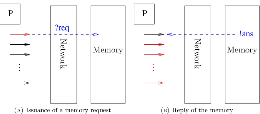
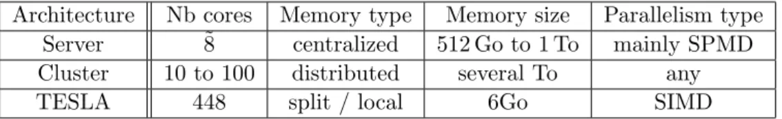
Since the processors does not communicate directly with the memory there is necessarily some time between the moment the processor emits a request to the memory and the moment it receives a reply for it. If the processor has to wait for the memory to reply, it will be dramatically slowed down. To address this issue we oriented our architecture towards massive megath-reading. The figure 10 illustrate this idea. When a thread has to read in memory9, the processor switches to another thread, and continues running,
9
P ?req Net w ork .. . Memory
(a) Issuance of a memory request
P !ans Net w ork Memory .. .
(b) Reply of the memory
Figure 10: When a thread (in red in 10a) sends a read request to the memory, the processor switches to the remaining threads (in red in10b) to hide the latency. When the processor switches back to the first thread, the answer from the memory has arrived in most cases. If a write request is issued, the processor does not have to wait for an answer from the memory.
switching threads when necessary, until it eventually switches back to the first one. If the answer from the memory has arrived, the thread will have virtually waited only one clock cycle for the memory to answer and the overall execution will not be delayed.
Processor
The processors needed for this architecture must support this massive thread-ing and quick context switchthread-ing. Our study has for now focused mainly on the network, but for further work, the processor could be the next part to be studied.
The registers of a processor reflect the state of the thread it is executing. We can know which instruction it executes and the memory that has been loaded. Usually, context switching is expensive because the state of the thread, those registers, have to be stored in memory, and another state has to be loaded. One way to perform this context switching would then be to duplicate those registers into an array of registers (figure11) so that each thread can switch back to its original state in no time, its registers having not been stored back in memory.
3.3 The network
3.3.1 Direct implementation of a multistage network
Multistage networks For a first architecture, we implemented the theo-retical design in a straightforward manner. Inspired by the NYU
Ultracom-Program Program Registers T1 T2 T3 T4 T5 P P Registers
Figure 11: In an SPMD (Single Program Multiple Data) architecture, all threads share the same program, they differ by the content of their registers (and thus by the memory they access). By duplicating the registers and giving each thread its registers, the processor can switch from one thread to another without being slowed down by memory accesses.
puter [GGK+83], we studied the different interconnection schemes used in MIMD. Given the number of elements we have to connect, crossbars, single bus and multiple buses architectures are not an option. Crossbars would be too expensive, since there would be millions of connections between the elements. Single and multiple buses on another hand would remain cheap, but the protocol to implement to avoid conflicts between elements to use the bus would be difficult. Moreover, all the memories would need to be present on all buses to be accessed from all processors.
P M P M P M P M P M P M P M P M P M P M P M P M P M P M P M P M
Figure 12: Pairs of processor–memory are connected together via a tree of buses. When the processors access in priority nearer memories, this structure limits the use of buses shared by all processors (the root of the tree). In our case however, each processor might want to access any memory, so there is a high probability of using the top bus, and the messages would be in fierce competition.
Let us consider the case of bus hierarchy (figure 12). This structure is very effective in MIMD architectures[Fly08]. Each processor has its own memory attached, and the pairs processor–memory are then grouped in clusters connected by a bus, in turn connected to other buses. Memory accesses are made in priority on neighbouring memories, so that each bus has fewer messages circulating. Unfortunately, and like in GPUs, in this system not all memories are treated equally as would be our goal, to abstract the shared memory into a single memory. If all memories were treated equally in this architecture, there would be many accesses to memories on other clusters and there would be bus contention, the transmission would be slowed down.
Therefore, we studied multistage networks first. One of those networks, the Omega network, was used in the NYU Ultracomputer[GGK+83]. With multistage networks, the number of network elements is greater than for buses but lesser than crossbars. The number of paths a message can take is greater than with buses and thus the probability of a conflict is lesser. There are different existing topologies, but to keep a simple one, we opted for a baseline network. Wu in [WF80] proved that baseline, omega and a couple of other networks are isomorphic, but in matters of connection we believe the baseline network has better properties for architecture repartition on cards, as is detailed in the appendixA.
Details of the architecture The network we implemented is an array of switches connected as in figure 13. Seen from a processor, the paths reaching the memories form a binary search tree, so the n layers first bits of the physical address design the memory on which the word is.
Processeurs
Mémoires
Figure 13: The baseline structure of the network. The number of processors and memory can vary, but since the addresses are random10, we must ensure that each
path leads to a memory, thus we need 2n layersmemories. On the other hand, we can have any number of processors, dispatched as we want, this is a parameter of the architecture. In red we see that the set of paths from a processor to the memories is a binary tree.
At each clock cycle, the switches transmit one of the messages on their input in both directions — from and to the processors — unless its output channels are full. When a message arrives on a switch, the first bit of the address is used to determine the direction to take and the message is transmitted to the next stage. The basic algorithm for the transmission follows. A more detailed description of the protocol can be found in the appendix B, for the sake of clarity.
if there is no message on input then do nothing
else if there is only one message on input then transmit it
else
if their destination channel is not the same then transmit both
else
3.3.2 Second architecture: a step further from theory
Motivation A lab of the CEA in Grenoble developed a technology that can do a multi-layered architecture (figure14). When we knew more about the specifications we started to work on an architecture designed for this technology.
Figure 14: In this architecture, the central CMOS can have connections between its two layers. Components connected on each face can then communicate via a complex network. (Image from a slide of the team)
This technology allows us to develop a 2D four-layered network. The two middle layers would be used to create two similar networks, and on each face we place processors and memories respectively. This architecture is currently in development so no results have been obtained yet.
Protocol presentation The global structure of the architecture can be seen in figure15. The processors send their message to the network which transmit it to the memories with the right destination coordinates by the shortest way. Since several such paths exist, we chose to limit it to one — by forcing the messages to first go vertically then horizontally — to ensure that two consecutive messages from the same source to the same destination always remain in the same order.
Finding the shortest path can be done by checking th most significant bit of the difference destination − position. For instance, if the network is 8 switches wide, and we are at position 010. If we want to go at position 111, the difference is 101, the most significant bit is 1, it is shorter to go left. If we wanted to go to 101, the MSB is 0, it is shorter to go right.
For now, each network layer has its own purpose, one for requests one for replies. But since there are more requests than replies — since write requests yield no reply — we believe that by inverting the used layer for every other processor, we would have better results.
Another improvement that could be implemented, although with diffi-culties in the simulation, would be to distinguish local variables of a thread from global variables at compilation time. With this knowledge, it would be possible to favour nearer memories when obtaining the physical address
P P P P MM MM MM MM P P P P MM MM MM MM P P P P MM MM MM MM P P P P MM MM MM MM
Figure 15: The two dimensional architecture (M stands for memory and P for processor). The processors are connected to the memories by a two-dimensional network. We consider this network is a torus, that is to say the components on opposite borders are connected. This way, each processor is at a maximal distance of the size of the architecture from each memory.
from the logical address. This way, we would have two advantages. Firstly, we would prevent unnecessary avoidable latency for those variables. But the main advantage is that by limiting the distance, the messages would remain in the network for less clock cycles, thus reducing the traffic and the transmission times.
4
Experimental results
4.1 Experimental setup
To test the robustness of this architectures sensitive part, that is to say the network, we developed a simulator in Python. This simulator purpose is to simulate the behaviour of each component of the architecture at clock level. The designer can define its components with little constraint — some constraints in the constructor and the need of two clock functions — to create a library of components, or they can reuse already existing components. At this level of description, specifying the component is the same as specifying the protocol. Then this library can be used to describe several architectures on separate files, which can then be run by the simulator. This process is described in figure16. A graphical interface has been added to visualize the architecture and to see where there is message congestion.
The visualization gives hints for optimization, notably for the best size for bounded channels, but the most meaningful information come from the logs. We seek to parametrize our architecture so as not to be slowed down.
Components library Architecture description
Simulator
Visualization LogsFigure 16: The simulator takes an architecture description as an input and give a textual description of what happens in the architecture. To check the architecture description and to localize potential hotspots visually, a graphical representation has been added. The architecture description uses a library of components known to the simulator.
In the logs, we can find in how much time a thread receives an answer from memory, and we can then extract statistics to study the impact of the different parameters on the global behaviour of the architecture.
4.2 First architecture
4.2.1 Components parameters
We implemented the network described in section3.3.1. In all our experi-ments, the memories are modelized by a component that puts requests in a queue and then treats them in a given number of clock cycle. In our ex-periments we opted for a latency of 3 clock cycles but in future exex-periments we shall test the impact of this parameter. Also, for a first approach, this queue is considered unbounded.
The processors on another hand are more complex components. We first implemented a “simple processor” where all processor have a single thread and no common program, then we implemented multithreaded processors sharing a common program. To limit the number of hotspots, we dispatch randomly the memory words in physical memory components, thus doing a hash of virtual addresses into physical addresses. We modelize this by using random addresses when the processor issues a request.
As parameters, the processors have a given probability of issuing a mem-ory request, either read or write, and then a ratio of read and write requests. According to [GHPR88], there is approximately 55% of memory requests, among which there are 1.7 times more read instructions. These values might have changed since then, but they are a good starting point for our simula-tions.
4.2.2 Results and analysis
We tested the architecture described by the file in the appendixD and its counterpart with independent processors. This architecture had the follow-ing properties :
• 1024 processors • 2048 memories • 23552 channels
• 100 threads of 50 instructions • program executed during 5000
cycles • 11 stages
• one stage transmits its message in one cycle
• messages stay in memory for 3 cycles
• approximately 2/3 of memory requests are loads
Number of cycles Minimum Maximum Median Mean Simple processors 26 118 33 35 26 383 63 78 SPMD 55% memory access 26 250 36 53 26 335 53 71 SPMD 25% memory access 26 133 28 30 SPMD 35% memory access 26 224 30 38 SPMD 45% memory access 26 164 29 32 SPMD 65% memory access 26 402 62 77 SPMD 75% memory access 26 616 49 85
Table 2: These statistics over transmission time of messages give an idea of how many threads a processor should run. Gross[GHPR88] studied that programs used approximately 55% of memory requests, so we first focused on this value.
We extracted statistics on how long took a read message to return to the processor. The results of this experiment take the form of graphs and statistical data summarized in table2.
With the graphs we can have a better understanding of the distribution of this time. By comparing the figures 17a and 17b we can see that the SPMD paradigm has the effect of delaying more messages. A first simple statistical analysis by analysing the statistical values tend to show that with independent processors and programs we have a chi-squared distribution and with SPMD processors with the same code we have a geometric distribution. Later more precise studies could be led to find more about the parameters of those distributions. The graphs corresponding to the runs in table 2can all be found in the appendixE.
The programs we tested had few instructions, to run faster. The statis-tics we have are representative of the program generated, not of all programs with the same parameters. We can see the results can vary in table 2 on the SPMD 55% line for instance. Nevertheless, before starting more precise statistics, those results give a first evaluation of the architecture.
4.2.3 Protocol presentation
The global structure of the architecture can be seen in figure15. The proces-sors send their message to the network which transmit it to the memories with the right destination coordinates by the shortest way. Since several such paths exist, we chose to limit it to one — by forcing the messages tu first go vertically then horizontally — to ensure that two consecutive mes-sages from the same source to the same destination always remain in the same order.
(a) Simple processors
(b) SPMD processors
Figure 17: Distribution of the number of messages given their transmission time. X-axis: transmission time, Y-axis: number of messages. When the processors all share the same program, they all tend to send requests at the same time, thus delaying the messages. Here the two architectures have the same parameters except the first has simple independent processors and the second uses SPMD processors.
4.3 Prospective results of the second architecture
As for now, the protocol of the second architecture is unfinished, and has bugs, we therefore cannot extract statistics. Currently, most messages do not return to the processors, but due to the late design, we did not have to time to debug it yet. The few messages that do arrive back to the processors have a rather high time of propagation, but due to the alpha stage of the protocol, we expect this time to decrease when the protocol is better defined. We also believe that a better use of the two layers of network, by making only half the processors use each layer, would lessen the transmission time.
5
Conclusion
To answer the needs of current bioinformatics challenges we designed and started to test two different architectures in which numerous processors are connected to a set of memories via a network. Since the communication between the processors and the memories through th network cannot be done instantaneously, we introduced massive megathreading to conceal the effect of latency, as the processors can run another thread while its requests are carried by the network. We studied the reaction of the network to different parameters, including the impact of the SPMD paradigm and the ratio of memory access instructions in a program. We needed to know if the latency induced remains acceptable and how many threads per processor are needed to conceal this latency. Our first results are rather encouraging. The observed transmission time of most messages was under 200 clock cycles even with a high probability of a memory instruction. Given we consider millions of threads split on a couple of thousands processors, the number of threads per processor should suffice to hide the latency induced by the network.
Of the two architecture models we tested, only one is currently fully operational, but both approaches already show strengths and limits. The main difference between the multistage design and the bidimensional design resign in its components repartition. In the former, the memories are all seen the same way from all processors, none can be favoured. The latter on the other hand has an inherent spatial locality which can become an asset. If a processor uses a nearer memory, the distance the messages have to cover would be shorter and they will stay in the network for a shorter time, thus reducing the load of the network. This is not possible in the first architecture. But on another hand, for farther memories, the transmission time becomes longer than for those observed in the first architecture, from our first measures. If further study confirm this trend, there will have a choice to make. Can we accept longer communication time for some requests if we speed up others or should all requests be treated equally? It is not possible to give a clear answer at this stage of the simulations since we lack
results on the second architecture.
We will therefore continue the study of those architectures to have more precise results and study some points that are yet to be considered.
The first major work in progress is to refine the protocol of each archi-tecture. The first architecture is already well defined but could still benefit from minor improvements and the second architecture is currently in an al-pha state. Fortunately, the simulator itself, which was developed jointly, has now reached a mature design and we can focus on the architectures. Once the protocol is well specified, we will run more experiments to yield more statistics. We would notably be interested in the global slowdown of the thread pool to evaluate the efficiency of the architecture. We will also study the influence of the different parameters on the results. We have already studied the impact the proportion of memory accesses, we can now change the bounds of the channels, the ratio of read/write accesses and the latency of the memories for instance.
Apart from the networks, the other components can be refined and lead to further study.One cause of the high latency is that a memory can only treat one request at a time. If the memory processes a request in 10 clock cycles, the fifth request in the waiting queue will be treated in 50 clock cycles. In further studies, we shall evaluate the impact of this phenomenon on the latency time. It might prove interesting to investigate the possibility to provide a memory with a reduced access time using more logic for instance. Another point related to memory is the randomization of the memory words. It is sometimes interesting to get more than one word from memory in one operation, when we want to access an array for instance. We might then wonder the granularity of the randomization process, to see the impact of a fine grain hashing when accessing structures that would normally be retrieved in one operation.
But the major component that should be studied next is the processor. To provide this megathreading, we need a processor able to switch from one thread to another in no time. At each clock cycle, the processor should be able to change its context to adapt to a new thread, in the fashion of “barrel processors”, which require further investigation. Given the number of threads, the processor will need many registers, and it might be impossible in practice to provide a cache large enough to be usable. Also, the current model of the processor generates a random program based on the given parameters. The next step of this model would be to execute real programs, or at least the load and store instructions. This way, we would evaluate the robustness of the network in real life situations.
Finally, the climax would be to eventually create the hardware, with reconfigurable devices for instance, to put it into real life tests, to validate all the work that we have done and that remains to do.
References
[Ans09] Wilhelm J. Ansorge. Next-generation DNA sequencing tech-niques. New Biotechnology, 25(4):195–203, April 2009.
[But07a] M. Butts. Ambric massively parallel processing arrays technology overview. Micro, IEEE, 27(5):32–40, 2007.
[But07b] M. Butts. Synchronization through communication in a massively parallel processor array. Micro, IEEE, 27(5):32–40, 2007.
[Col10] Sylvain Collange. Enjeux de conception des architectures GPGPU : unit´es arithm´etiques sp´ecialis´ees et exploitation de la r´egularit´e. PhD thesis, Universit´e de Perpignan, November 2010.
[FB09] S. Furber and A. Brown. Biologically-inspired massively-parallel architectures-computing beyond a million processors. In Appli-cation of Concurrency to System Design, 2009. ACSD’09. Ninth International Conference on, pages 3–12, 2009.
[Fly08] Ola Flygt. Computer architecture : Shared memory mimd architectures.
http://w3.msi.vxu.se/users/ofl/DA2022/Material/CH18. pdf, 2008.
[GGK+83] A. Gottlieb, R. Grishman, C.P. Kruskal, K.P. McAuliffe, L. Rudolph, and M. Snir. The NYU Ultracomputer – Designing an MIMD Shared Memory Parallel Computer. IEEE Transactions on computers, pages 175–189, 1983.
[GHPR88] Thomas R Gross, John L Hennessy, Steven A Przybylski, and Christopher Rowen. Measurement and evaluation of the MIPS architecture and processor. ACM Transactions on Computer Sys-tems (TOCS), 6:229–257, August 1988. ACM ID: 45060.
[Gue10] Alexandre Guerre. Approche hi´erarchique pour la gestion dy-namique des tˆaches et des communications dans les architectures massivement parall`eles programmables. PhD thesis, Facult´e des sciences d’Orsay, Universit´e Paris-Sud 11, September 2010. [Hal06] T. R. Halfhill. Ambric’s New Parallel Processor, 2006. [inta] Intel research :: Single-Chip cloud computer.
http://techresearch.intel.com/ProjectDetails.aspx?Id= 1.
[intb] Intel unveils new product plans for High-Performance computing.
http://www.intel.com/pressroom/archive/releases/2010/ 20100531comp.htm.
[Law75] D.H. Lawrie. Access and alignment of data in an array processor. IEEE Transactions on Computers, pages 1145–1155, 1975. [Mar08] Elaine R. Mardis. The impact of next-generation sequencing
tech-nology on genetics. Trends in Genetics, 24(3):133 – 141, 2008. [NVI10a] NVIDIA. CUDA Best Practices Guide Version 3.0, February
2010. CA Patent 95,050.
[NVI10b] NVIDIA. programming guide version 3.0, 2010.
[THL09] D. B Thomas, L. Howes, and W. Luk. A comparison of CPUs, GPUs, FPGAs, and massively parallel processor arrays for ran-dom number generation. In Proceeding of the ACM/SIGDA in-ternational symposium on Field programmable gate arrays, pages 63–72, 2009.
[WF80] C.L. Wu and T.Y. Feng. On a class of multistage interconnection networks. Computers, IEEE Transactions on, 100(8):694–702, 1980.
A
Three dimensional conception
One side concern was to design an architecture that could be inplemented in a three dimensional way. When I started working on the multistage networks I tried to visualize in three dimensions how it would be possible to implement — quite a mind torturing activity I have to say. To ease this work, I tried to create a model in 3D with the software Blender, the result can be seen in figure 18. The network is already a baseline network. At each stage, the network is divided into two blocks, one for each bit in in the address. We represented these blocks giving a different color for each stage. In the end, we can see there remain one block per “layer”. This way, the baseline network proved to be a binary tree ideal for addressing layers.
Figure 18: This representation of a baseline network show that the baseline net-work enables addressing of different layer while keeping a good separation of each path. The different stages of the network are represented in different colours.
A second interpretation of the 3 dimensional goal is the repartition on different layer or cards. Again, the baseline network shows good properties. Indeed, after log2n cards layers, there is no more connexion between cards, as can be seen in figure19.
Figure 19: At each stage of the baseline network the number of distant connections is reduced, thus simplifying its integration on multiple cards
B
Protocol for each component
We here call request the sending of a message from a processor to the mem-ories and reply the message from a memory to the processors. An example of switch has been given at figure 20. The names are taken with a request convention, since all channels are bidirectional.
in0
in1
out0
out1
Figure 20: A switch is mainly a router from two inputs to two outputs. In our architecture, the four channels are bidirectional.
B.1 Messages
A message can be described by four characteristics:
Function Describes if the message shall be interpreted as a memory read, write, or some more complex operation
Source adress Contains the adress of the processor from the point of the network where the message is. When the message is produced by the processor, this is an empty word.
Destination adress Contains the adress of the memory word from where the message is in the network again. When the message leaves the mrocessor, this is the virtual adress, and when it reaches the memory, it is the physical adress in it. It can be divided into two parts: the adress of the memory and the adress of the word in the memory. Data Data associated with the function. The value to write in memory or
the number of contiguous words to read for a request or the value read for a reply, for instance.
It is important to note that a message can be divided into a header (function and source and destination adresses) and the data. The headers size does not vary, since as the message goes from the processors to the memories, the size of the memory adress decreases as much as the source adress increases — and reciprocally for a reply.
B.2 Channels
As mentioned in the previous subsection, inputs and outputs of switches — but not only, memories and processors too — are modeled by bidirectional FIFO channels. Those channels may have a bound that can vary according to the direction. For the first simulations, the channels will be unbounded. The basic operations on the channels are:
read: Reads the first message of the channel without removing it. write: Writes a message at the end of a channel.
pop: Deletes the first message of the channel. B.3 Switches
A switch can route the messages from its inputs to its outputs for a request and the other way for a reply. The messages coming from all four arriving channels are analysed (read), and those that can be transmitted are removed from their channels (popped) and written on the right outgoing channel11.
When a message is transmitted on a request (resp. reply), the first symbol of its destination (resp. source) is used and popped to know its target channel and the number of the input (resp. output) channel it comes from is added to the source (resp. destination). This way, at any moment, it is possible to know how to go either to the processor it comes from or the memory it is bound to.
The switch can take different configurations depending on the messages incoming.
B.3.1 Normal routing
When only one channel yields a message, it can be routed without problem. For instance, on a request, if the message’s destination starts with a 0, it will be routed to out0. The four possible configurations are listed in figure21.
If two messages are read with different destinations — from the point of view of the switch, that is to say they will be written in different channels — they can be routed independently one from the other. We thus have the two situations depicted at figure22.
B.3.2 Multicast
When two messages want to read the same word in memory, it is possible to collapse the two messages to limit the number of messages in the network. When such a case happens, instead of writing ’0’ or ’1’ in the source field, a special symbol is written, that we denote ’x’, and only one message is
11
in0 in1 out0 out1 in0 in1 out0 out1 in0 in1 out0 out1 in0 in1 out0 out1
Figure 21: Routing of a single message. The process is symmetric for a request or a reply. For instance, in the upper right situation, for a request, ’0’ has been read in the messages destination, and ’1’ has been appended to its source before being transmitted.
forwarded. On the reply, when a ’x’ is read, the message has to be routed to both in0 and in1. The situation is summarized in figure23.
B.3.3 Conflicting transmission
When two messages should write on the same channel without accessing the same word for reading ends in a conflict. Three types of conflicts exist: Read-Read (RR), Read-Write (RW) and Write-Write (WW). The behaviour on a RW and a WW conflict has yet to be studied.
On a RR conflict, one of the messages only is transmitted, as in a normal routing (figure21). The other message is delayed, and shall try again to be transmitted at next clock cycle. The message to be transmitted is chosen by an unspecified arbiter, though we consider a random arbiter for our model, since we believe it will have good properties.
in0 in1 out0 out1 in0 in1 out0 out1
Figure 22: Transmission of two messages without conflict. It works like a single message transmission for each message.
in0 in1 out0 out1 in0 in1 out0 out1
Figure 23: Multicasting of messages. The message is forwarded from one input only but the answer will be redirected to both.
B.3.4 Pseudo-code protocol
In this section we will first define what transmitting a message is: if the target channel is full then
do nothing else
update the source and destination of the message write the message in its target channel
The protocol for a request is then: if there is no message on input then
do nothing
else if there is only one message on input then transmit it
else
if their destination channel is not the same then transmit both
else if the message can be multicast then transmit one
forget the other else
transmit one ; /* the other is delayed */
The protocol for a reply it very similar: We must note that in the case if there is no message on output then
do nothing
else if there is only one message on output then transmit it
else
if one message is a multicast then
transmit one ; /* the other is delayed */
else if their destination channel is not the same then transmit both
else
transmit one ; /* the other is delayed */
of a multicast reply, the message is transmitted if and only if none of the destination channels (in0 and in1 in this case) is full. We do not transmit a multicast in two parts.
C
Example of transmission
We have a switch with no input on in0 and a message on in1 (request) with the header defined as the following:
src 1110 dst 011101001 function 00 (read)
Since src is of size 4 we know we are at the fifth layer of switches (we passed 4 already). The representation of the header can be represented as in order:
1. the function 2. the dst
3. the mirror of the src
The reason we use the mirror is that it is easier to add the number of the input to update the src.
Here, our header would be : 00 011101001 0111. The function will not be changed so we will concentrate on the two other parts. To know where the message is headed, we read the leftmost bit. Here it is 0 so the message will be written on output out0.
The new addresses are produced by applying : addr = (addr << 1) | input_number. Here the input is in1 so the addresses fields become, concatenated : 1110100101111.
All is summarized in figure24. If the message were a reply rather than a request, it would have been symmetric: read the rightmost bit, shift to the right and set the third bit of the resulting header to the output number.
in0 in1 out0 out1 Message: function: 00 Addresses: 0111010010111 Message: function: 00 Addresses: 1110100101111
Figure 24: Transmission of a message. This can be read either from the left to the right or from the right to the left.
D
Example of architecture description
from b a s e l i n e import q B a s e l i n efrom math import l o g from g r a p h i c a l import ∗ N = 2048 LN = i n t ( l o g (N, 2 ) ) p r o c e s s o r s = [ ] memories = [ ] # c r e a t e s a c h a n n e l i f n e c e s s a r y def chan ( p ) : i f p == None : return qBiChannel ( s c e n e ) e l s e : return p . c h a n n e l # i n s t a n c i a t e h a l f a s p r o c e s s o r s a s memories f o r i in x r a n g e (N/ 2 ) : p r o c e s s o r s . append ( s e l f . i n s t a n c i a t e ( ’ qSimpleSPMD ’ , s e l f . s c e n e , 0 , i , 5 0 , 1 0 0 , 0 . 7 5 , 2 0 , 1 0 , boundRequest = 3 , boundReply = 3 ) ) p r o c e s s o r s . append ( None ) # c r e a t e s t h e b a s e l i n e n e t w o r k # t h i s f u n c t i o n i s d e f i n e d i n a n o t h e r f i l e
o u t p u t s = q B a s e l i n e ( s e l f , map( chan , p r o c e s s o r s ) , 1 , 0 , bound = 3 )
# i n s t a n c i a t e s t h e memories and c o n n e c t s them t o t h e e x i s t i n g c h a n n e l s
f o r i in x r a n g e (N ) :
memories . append ( s e l f . i n s t a n c i a t e ( ’ qMemory ’ ,
s e l f . s c e n e , LN + 1 , f l o a t ( i ) / 2 . , 2 , o u t p u t s [ i ] , boundRequest = 3 , boundReply = 3 )
)
E
Statistics
E.1 Some statistics for 5000 cycles, with 2048 memories and 1024 processors
• 1024 processors • 2048 memories • 23552 channels • 5000 cycles • 11 stages
• 1 cycle per stage
• messages stay in memory for 3 cycles
• 55% of memory instructions, 2/3 of which are loads
• channels buffer size : 3 E.1.1 Simple processor (random instructions)
There were 710 tries to write in a full channel.
A total of 1761388 messages returned to the processors.
Distribution of the number of messages given their transmission time. X-axis: trans-mission time, Y-axis: number of messages. Mean : 35 Median : 33 Maximum : 118 Minimum : 26 Variance: 64
E.1.2 Simple SPMD (no branches, random adresses) First run A total of 1686606 messages returned to the processors.
Distribution of the number of messages given their transmission time. X-axis: trans-mission time, Y-axis: number of messages. Mean : 78 Median : 63 Maximum : 383 Minimum : 26 Variance: 2570
Second run A total of 1403450 messages returned to the processors.
Distribution of the number of messages given their transmission time. X-axis: trans-mission time, Y-axis: number of messages. Mean : 53 Median : 36 Maximum : 250 Minimum : 26 Variance: 1070
Third run A total of 1506022 messages returned to the processors.
Distribution of the number of messages given their transmission time. X-axis: trans-mission time, Y-axis: number of messages. Mean : 71 Median : 53 Maximum : 335 Minimum : 26 Variance: 2431
E.2 Varying the number of memory accesses
The parameters are the same as before except the number of memory ac-cesses.
25% of memory accesses. X-axis: transmission time, Y-axis: number of messages. Mean : 30 Median : 28 Maximum : 133 Minimum : 26 Variance: 62
35% of memory accesses. X-axis: transmission time, Y-axis: number of messages. Mean : 38 Median : 30 Maximum : 224 Minimum : 26 Variance: 493
45% of memory accesses. X-axis: transmission time, Y-axis: number of messages. Mean : 32 Median : 29 Maximum : 164 Minimum : 26 Variance: 110
55% of memory accesses. X-axis: transmission time, Y-axis: number of messages. Mean : 53 Median : 35 Maximum : 256 Minimum : 26 Variance: 1167
65% of memory accesses. X-axis: transmission time, Y-axis: number of messages. Mean : 77 Median : 62 Maximum : 402 Minimum : 26 Variance: 2455
75% of memory accesses. X-axis: transmission time, Y-axis: number of messages. Mean : 85 Median : 49 Maximum : 616 Minimum : 26 Variance: 5373


![Figure 7: This image from [Fly08] summarizes the different choices for shared memory MIMD architectures](https://thumb-eu.123doks.com/thumbv2/123doknet/5461450.129179/15.892.179.728.189.596/figure-image-summarizes-different-choices-shared-memory-architectures.webp)