HAL Id: hal-01588445
https://hal.archives-ouvertes.fr/hal-01588445
Submitted on 15 Sep 2017HAL is a multi-disciplinary open access archive for the deposit and dissemination of sci-entific research documents, whether they are pub-lished or not. The documents may come from teaching and research institutions in France or abroad, or from public or private research centers.
L’archive ouverte pluridisciplinaire HAL, est destinée au dépôt et à la diffusion de documents scientifiques de niveau recherche, publiés ou non, émanant des établissements d’enseignement et de recherche français ou étrangers, des laboratoires publics ou privés.
Racetrack micro-resonators based on ridge waveguides
made of porous silica
Pauline Girault, Nathalie Lorrain, Jonathan Lemaitre, Luiz Poffo, Mohammed
Guendouz, Isabelle Hardy, Michel Gadonna, Aldo Gutierrez, Loïc Bodiou,
Joël Charrier
To cite this version:
Pauline Girault, Nathalie Lorrain, Jonathan Lemaitre, Luiz Poffo, Mohammed Guendouz, et al.. Race-track micro-resonators based on ridge waveguides made of porous silica. Optical Materials, Elsevier, 2015, 50 (part B), pp.167-174. �10.1016/j.optmat.2015.10.017�. �hal-01588445�
1
Racetrack micro-resonators based on ridge waveguides made of porous silica.
P. Girault1, N. Lorrain1*, J. Lemaître1, L. Poffo1, M. Guendouz1, I. Hardy2, M. Gadonna2,
A. Gutierrez1, L. Bodiou1 and J. Charrier1
1
UMR FOTON, CNRS, Université de Rennes 1, Enssat, F22305, Lannion, France
2
UMR FOTON, CNRS, Institut Mines Telecom, Telecom Bretagne, F29238, Brest, France
* Corresponding author: [email protected]
Abstract
The fabrication of micro-resonators, made from porous silica ridge waveguides by using an
electrochemical etching method of silicon substrate followed by thermal oxidation and then by a
standard photolithography process, is reported. The design and fabrication process are described
including a study of waveguide dimensions that provide single mode propagation and calculation
of the coupling ratio between a straight access waveguide and the racetrack resonator. Scanning
electronic microscopy observations and optical characterizations clearly show that the
micro-resonator based on porous silica ridge waveguides has been well implemented. This porous
micro-resonator is destined to be used as an optical sensor. The porous nature of the ridge
waveguide constitutes the detection medium which will enhance the sensor sensitivity compared
to usual micro-resonators based on the evanescent wave detection. A theoretical sensitivity of
1170 nm per refractive index unit has been calculated, taking into consideration experimental
data obtained from the optical characterizations.
2
1. Introduction
Porous silica is obtained from a total oxidation of porous silicon (PS) which allows to obtain
transparent porous silica with low waveguide optical losses [1, 2]. PS is easily fabricated by
electrochemical[3] etching of silicon. The tunability of the porosity and of the thickness of PS
layers which depends on fabrication parameters, allows optoelectronic components [4], filters
[5,6], sensors for chemical [7, 8], biological [9,10,11,12,13] applications to be developed.
Indeed, the large internal surface of PS and its biocompatibility are significant advantages for
biosensing applications [11]. However, as the surface of PS is strongly hydrophobic, thermal
oxidation and chemical adaptation must be applied respectively to stabilize and functionalize the
internal surface of the porous silicon layer to obtain subsequent efficient molecules attachment.
The oxidation of PS has been extensively investigated by several authors in order to fabricate
SOI structures or to form a dielectric isolation material for IC components [14] or integrated
optical waveguides [15].
The partially or totally oxidized PS material can be used as a host for various molecules
which can either be in solution in the pores, or grafted onto the internal surface after the
functionalization of the PS [10]. In most cases, these molecules can be detected by a change in
the refractive index of the porous material, induced by their presence inside the pores. Indeed,
the refractive index is a weighted average of the refractive index of silicon (if partial oxidation),
silica, and the components inside the pores (molecules, air…). For small sized pores (less than
the optical sensing wavelength) the effective medium method can be used to estimate the
refractive index of the PS, which can be even partially or totally oxidized (porous silica), and the
3 Optical sensors based on PS using refractive index variations [11] have already been the
subject of several studies, the number of which continues to grow due to the interest of this
material for increasing the sensor sensitivity. Among components based on PS partially or totally
oxidized, microcavities sensors [9,17,18],Bragg reflectors[8] and planar ARROWs [19] do not
need any photolithographic steps for fabrication as only vertical light confinement is required.
Other optical structures have been developed with both lateral and vertical confinement using
photolithography processes [20, 21]or a direct laser writing method [22]; for example, buried
waveguides have been used to fabricate integrated Mach-Zehnder interferometers for sensing
applications [23, 24]. Recently, the first single side coupled micro-ring resonator based on PS
[25] has been fabricated using standard electron beam lithography and reactive ion etching. The
porous core ridge waveguide height was 600 nm. The highest sensitivities of optical sensors
based on PS reported to date are obtained from spectral measurements of resonant cavities [26]
(300-500 nm per Refractive Index Unit (RIU)) or of grating coupled waveguides (1000 nm/RIU)
[12] made using electron beam lithography and reactive ion etching for the detection of peptide
nucleic acid (PNA).
Micro-Resonators (MRs) for sensing applications are now being widely investigated as they
offer the advantage of significant miniaturization of the device, which greatly reduces the
number of molecules needed for detection [27, 28].
The best Q factors, better than 107, are obtained with microsphere resonators using
whispering-gallery mode (WGM) resonances [29, 30]. The WGM have a large potential for
sensing application with very low optical detection limits as they are able to react to a monolayer
4 However, microsphere resonators lack integration capability [32], which limit their use in
practical applications. To solve these problems, integrated micro-ring, racetrack or micro-disk
resonators are used, albeit with reduced Q factors [33]. In integrated optics, the Q factor is
limited in the range of 104 - 105 because of the optical losses into the resonators due mainly to
the material and the technological process.
Silicon and polymers are the main materials used in the fabrication of integrated resonant
structures, which rely on the evanescent waves to detect the presence of molecules whether
adsorbed on the sensor surface (surface sensing) or spread into the surrounding medium
(homogeneous sensing) [34].
However, the sensitivity of integrated MRs can be improved by optimizing the interaction
between the molecules and the optical wave. This optimization can be provided by the use of a porous waveguide core that will allow a direct interaction between the propagated light and the
molecules to be detected [12]. Mancuso et al. [35] have used a nanoporous polymer for
waveguide MRs cores, allowing an increase in the device sensitivity of 40 %.
In the present work, fully oxidized PS (or porous silica) will be used for the core of the MR
waveguides so as to greatly enhance the interaction between the propagated light and detected
molecules and thus the sensitivity. The first all PS single side coupled micro-ring [25] with ring
radii of 10 or 25 µm and a gap between the ring and the straight waveguides of 200 nm, gave a
detection sensitivity of 380 nm/RIU when salt water solutions infiltrated the device. Besides, a
theoretical study of a PS micro-ring resonator with a rib waveguide geometry has been
performed by Hutter et al [36]. Their study clearly demonstrated the potential of a PS micro-ring
for sensing application with a single ring resonator. An improved sensitivity of 700 nm/RIU was
5 design and a detection mode based on evanescent waves. Higher values could be reached by
using a cascade of micro-resonators[37] or by an integration of micro-resonators into a Mach Zehnder interferometer [38].
For the conception of a MR, low loss waveguides supporting single-mode propagation are
required [28]. The design can be horizontal, the most widely used because its simplicity, or
vertical, which requires several photolithographic mask levels [39]. For a horizontal design,
lateral flanks of the core waveguides have to present a rectangular section in the coupling region
for the control of the coupling ratio between a straight access waveguide and a resonator
waveguide. Up to now, porous silica buried single mode waveguides have been fabricated with
losses from about 1 dB/cm[22] to 4 dB/cm[40] but the lateral flanks were not vertical but were
slightly rounded.
To date, no rib based on partially or totally oxidized PS single mode waveguide with vertical
lateral flanks and with a height larger than 1 µm has been fabricated.
In this study we demonstrate the feasibility of the fabrication of a racetrack MR based on
porous silica ridge waveguides using standard photolithographic patterning with a polymer
photoresist. In the first part, we present the fabrication method and the characteristics of the
porous silica layers obtained. Then the photolithography method implemented to elaborate the
racetrack micro-resonator based on ridge waveguides made of porous silica is described. In a
second part, we detail calculation methods that we have implemented to get the waveguide
dimensions required for single mode propagation and to determine the coupling ratio between
the straight and the racetrack ridge waveguides. Then, the design of the MRs based on ridge
waveguides made of porous silica is detailed including the waveguide dimensions for single
6 are structurally and optically characterized. As the MRs will be used for sensing application, we
also present a preliminary theoretical study of the porous MRs sensitivity.
2. Material and Implementation method 2.1. Porous silica layers
Three consecutive PS layers were prepared by electrochemical anodization of a heavily doped P
substrate with three successive current densities of 4, 50 and 100 mA/cm² for specific times. The
electrolyte was composed of (50 %) HF, ethanol and deionized water solution with ratios of
2:2:1 respectively. Following this, the PS layers were completely oxidized at 960 °C for 1 hour
under a humid oxygen flow in order to obtain porous silica layers. The first porous (upper) layer
(4 mA/cm²) presents a low porosity (around 6 %) and plays the role of a “technological barrier”
that prevents the other deeper porous silica layers from being infiltrated by the resin during the
subsequent photolithography process which is necessary to create the ridge porous waveguides.
The second (50 mA/cm²) and the third (100 mA/cm²) porous layers constitute the core and the
lower cladding layers respectively of the porous silica waveguides.
The porosity and the refractive index of the core and cladding silica porous layers were extracted
using the Bruggeman model from reflectivity spectra of two single porous layers whose
fabrication parameters corresponds to the core and the cladding respectively [2, 17]. The
accuracy of 60 nm on the thicknesses of the single porous layers induces errors of 5 % and 0.02
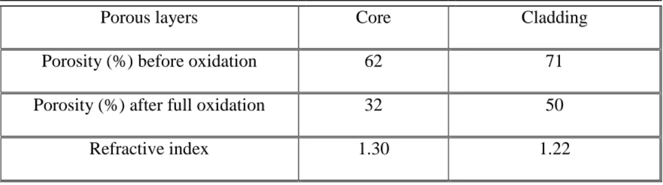
7 The values of porosities and refractive indices of the core and the cladding porous silica
layers are given in Table I. We also have mentioned the porosity of the porous silicon layers
before their full oxidation.
Table I: Porosity of the PS layers before oxidation and photolithography steps. Porosity and
refractive index at 1550 nm for the porous silica ridge waveguide structure.
Porous layers Core Cladding
Porosity (%) before oxidation 62 71
Porosity (%) after full oxidation 32 50
Refractive index 1.30 1.22
As in ref [2], the adjustment of theoretical and experimental reflectance spectra is obtained by
considering a total oxidation of the porous silicon layers. Moreover, the use of the M-lines
method have also shown the same indices taking into consideration the accuracies of
measurements. Besides, as mentioned in reference [14, 41], as the porosities of the core and the
cladding layers are, before the oxidation step, higher than 56 % (table I), a full oxidation of PS is
obtained. However, a slight difference in the stoechiometry compared to silica could occur [42],
Beside, according to Yakovtseva et al [15], with the use of a temperature of 800-900°C, the
quality of the material obtained is still different from that a standard thermal SiO2.
Yet, as the effect on the change in the indices is lower than the accuracies of the measures, we
8
2.2.Photolithography process
The ridge porous waveguides were then created using a standard photolithography process on
the porous silica layers. The process is described for a straight waveguide in Fig. 1. A positive
SPR photosensitive resin layer was deposited by spin coating on the top of the structure. Patterns
were then produced under UV exposure through a well-defined chrome mask designed using
Olympios software.
To obtain the desired ridge waveguides, a trifluoromethane (CHF3) plasma RIE (Reactive Ion
Etching was performed. Carefully checking was required to be sure that the resin had not
infiltrated the pores through the first low porous layer (barrier porous silica layer) during the
photolithography process. In order to verify this step, the method used relies on reflectivity
measurements of a single porous layer obtained with the same anodization parameters (4
mA/cm²) as the porous barrier layer, without and with the resin deposit.
Fig. 1. Schema of the photolithography process used for the fabrication of porous silica
9 exposure; b) wet etching development of the photosensitive resin; c) dry etching of the
porous silica layers (“technological barrier” and core) under the unprotected area.
To obtain a good resolution, the thickness of the photosensitive resin has to be the thinnest.
Yet, it has to be thick enough in order to allow the etching of the core layer before the complete
etching of the photosensitive resin without which the patterns are not well defined. The
selectivity, the ratio between the etching rate of the photosensitive resin and the core layer
(shown in table II), has to be the highest. By adjusting RIE parameters, we experimentally
obtained a selectivity around 5. Then, knowing the selectivity, we have to adjust the resin
thickness in order to get a target core thickness at the end of the process.
Table II: RIE dry etching rate for the different layers
Layers in the photolithography
process
Resin SPR Porous silica core Porous silica cladding Photolithography etching rate (nm/s) 50 250 500 3. Calculation methods
3.1 Waveguide dimension range for single mode propagation
The dimensions of the porous silica core waveguide have to be chosen to provide single
mode propagation at 1.55 µm. The effective refractive index method [43] and Matlab software
were used to calculate the effective refractive index of the ridge porous silica waveguide as a
10 mode, the 01 mode and the 10 mode. Then, the lowest dimension limits (width and height) that
involve solutions to the Maxwell equations [43] for these TE and TM modes propagation, were
deduced. The possible dimensions of the ridge waveguides required to obtain only single mode
(00 mode) propagation for both the TE and TM modes, are between the lower limit dimensions
of the 00 mode and the lower limit dimensions of the 01 and the 10 modes.
3.2 Calculations of the coupling ratio between access and micro-resonator waveguides
The MR configuration which has been studied is a single side coupled racetrack
resonator. Fig. 2.a represents the top view of the coupling area that has been considered and
which includes the straight waveguide and half of a racetrack waveguide.
The separation (gap) “g” between the straight waveguide and the MR is an important
parameter which contributes to the coupling ratio. In order to calculate the coupling ratio for a
range of gaps studied, we have used the method described in the following for both the TE and
TM modes.
Fig. 2.b is a schematic cross section which shows the straight and the ring core waveguides
(refractive index n1) surrounded by the lower (refractive index n2) and upper cladding (refractive
index n3) layers at the minimal gap “g”.
In this configuration, the gap between the straight and the racetrack waveguide is a constant in
the z axis only along the straight coupling area (distance Lc).
In the y direction, in the curved coupling area, the distance separation between the straight
and the racetrack waveguides, as a function of z, can be expressed by the following equation:
11 where g is the minimal distance between the straight and the racetrack waveguides, Re is the
extern radius and , defined by
e
R z arcsin
θ , varies from to .
Fig. 2. Schema of the coupling region of racetrack resonator: (a) top view and (b) cross
section view at z = 0.
We note that CT(z) the coupling coefficient for a z abscissa, given in the Marcatili method
12
where:
- a is the core waveguide width (in the y transverse direction),
- kz is the axial propagation constant which depends on the transverse propagation
constants kx and ky, and on the propagation constant k1 in the free space medium of
refractive index n1; the constant kz, kx and ky for the TE and TM modes can be
expressed by:
The transverse propagation constants kx and ky depend on the refractive indices (Fig. 2.b)
of the core (n1), the lower (n2) and the upper cladding (n3) layers of the waveguides and on the
13
Then to obtain the coupling coefficient Cw over the whole distance of the coupling area (Fig.
2.a), the CT(z) function has to be integrated between
and Re and then multiplied by a factor
2 because of the symmetry of the geometry:
Then the coupling ratio is equal to[43]:
4. Results and discussion
4.1 Design of the all porous silica micro-resonator
4.1.1. Waveguide dimension range for single mode propagation
Using the method described in the part 3.1, the lowest dimension limits (width and height)
that involve solutions to the Maxwell equations [43] for the TE00, TE01 and TE10 modes
14 Fig. 3. Solutions of the Maxwell equationsfor the TE00, TE01 and TE10 modes as a function
of the porous silica ridge waveguide dimensions. The grey area between the TE00
fundamental mode curve and the TE01 and TE10 modes curves represents the waveguide
dimensions range for which only single mode propagation is possible.
The grey area between the lowest limits of the TE00 mode (fundamental mode) and the TE10
and TE01 modes, represents the single mode region. For TM modes, the curves are similar to TE
modes but are slightly shifted towards higher dimension values. Based on these results, the
waveguide width could be between 1.5 µm and 3.5 µm so that a wide range of height (typically
from about 1 µm to 3 µm) could allow single mode propagation. In this dimension range, we
have chosen to experimentally target a waveguide width of 2 µm and a height waveguide of 2.5
µm. Then, for these chosen dimensions, an effective refractive index of 1.238 ± 0.020 for the TE
mode and 1.243 ± 0.020 for the TM mode were calculated using the effective index method [43].
Similar values were obtained from the Finite Difference Generic (FDG) method which is a
15 refractive indices take into account the measurements errors on the refractive index of the core
and cladding porous silica layers.
4.1.2. Coupling study between the access and the porous micro-resonator waveguides
Since the porous silica MR will be used for sensing applications, the MR is designed as a
racetrack with a radius R of 25 µm in order to obtain a free spectral range superior to
5 nm which is sufficient enough to get a large detection window. Furthermore, to obtain a
sufficient coupling ratio between the straight and the curved waveguides, different coupling
length Lc have been studied (0, 30, 40, 50, 60 and 70 µm). Considering that the theoretical
resolution limit of photolithography is 0.4 µm for polymer materials [45], gaps varying from 0.5
to 1 µm have been studied.
Using the calculation method defined in part 3.2, the coupling ratio κ2
has been calculated at
= 1550 nm as a function of the gap “g” for a waveguide width of 2 µm and a height of 2.5 µm for different studied coupling lengths Lc.
For a coupling length of Lc = 70 µm and within the studied gap range (0.5 µm to 1 µm) that
can be obtained from a process point of view, the coupling ratio varies from 8 % to 90 % for TE
16 Fig. 4. Calculated coupling ratio as a function of the gap between the straight and the
curved waveguides for the TE and TM modes for a waveguide width of 2 µm at 1550 nm
(R = 25 µm and Lc = 70 µm).
For this case, the range of gap studied here allows us to reach a wide scale of coupling ratios
that should be sufficient to obtain good MR transmission spectra.
In Fig. 5, the top view (a) and the cross section (b) of the porous silica racetrack MR design
are reported with the chosen waveguide dimensions and the MR geometry that provide a
sufficient coupling ratio (Lc = 70 µm) and a sufficient free spectral range which is in this case of
17 Fig. 5. Schema of a top view (a) and a cross section (b) of the porous silica racetrack MR.
4.2.Control of manufacturing process
Scanning Electronic Microscopy (SEM) images of the ridge racetrack porous MR are
presented in Fig. 6. The cross section of the etched waveguide in Fig. 6.a shows a waveguide
core, the height of which is 2.5 ± 0.1 µm. The core is rectangular only in its lower half, with a
width of 1.8 µm instead of the 2 µm expected from the photolithography mask. During the
photolithographic step of etching the top of the porous layers, the edges of the ridge waveguides
are also affected, more so in the top half, which explains the width profile.
The SEM top view of the whole structure is given in Fig. 6.b. At this magnification, the
racetrack is well defined and with the target dimensions. The separation between the straight and
the racetrack MR ridge, constituting the coupling region, has been well achieved. At a high
18 width of 1.8 µm ± 0.1 µm, appears in light grey whereas the cladding layer shows as dark grey in
the SEM image.
Fig. 6. SEM images of the racetrack resonator: (a) cross section of a porous silica
waveguide; top views at different scales: (b) whole racetrack MR, (c) the two waveguides
in the coupling area, (d) the gap separation between the two waveguides of the coupling
area.
In Fig. 6.d, the pores are visible and have larger dimensions in the cladding layer than in the
core layer, in accordance with their respective porosities. The gap between the straight
waveguide and the racetrack waveguide is 0.8 µm ± 0.1 µm instead of the 0.6 µm expected. The
real separation distance between the two waveguides is higher than expected by 0.2 µm because
19
4.3. Transmission responses of the porous silica racetrack MR
In order to verify that the porous silica racetrack MR is optically operational, the spectral
transmission responses, for different gaps, were measured. The output from a tunable wavelength
laser is injected in the input straight waveguide using a lensed fiber with a mode radius of 2.2
µm. A second lensed single mode fiber is also used to couple the output of the straight
waveguide to a power meter or to an optical spectrum analyzer. A polarization controler was
inserted between the output of source and the first lensed fiber. The transmission measurements
were done with a step resolution of 1 pm over the wavelength range of 1545-1560 nm at the
output of the straight waveguide. The measured transmission as a function of the wavelength for
one polarization of light is reported in Fig. 7 for the experimtental gap of 0.8 µm. The spectrum
shows two resonance wavelengths at 1549 nm and 1555 nm in the range studied. This
demonstrates that the light is propagated in the waveguide and in addition, good coupling of the
light occurs between the access waveguide and the MR. This experiment shows clearly that we
have succeed in making a ridge porous silica racetrack MR.
Fig.7. Experimental transmission spectra for one polarization of light. In the insert, the
20 From the experimental transmission spectra (Fig. 7), the following characteristics of the
resonator that we have already described in reference [46] have been deduced, with the same
assumption that the coupling losses are negligible : an extinction ratio of around 6.5 dB, a Free
Spectral Range (FSR) of 5.6 nm which is of the order of magnitude expected, taking into account the geometry of the design and the effective index. A full width at half maximum (δλ) of 0.45
nm is obtained, with a corresponding quality factor Q of 3392.
Using the equations defined in our previous study on polymer micro-ring resonators[47], the
theoretical transmission has been calculated and then adjusted to match the experimental one.
The adjustment of the resonance shape (insert in Fig. 7) is performed by modifying the coupling
ratio and the propagation losses in the ring, whereas the FSR is adjusted with the group index
parameter. A coupling ratio κ² of 32.5 ± 1.0 % and a field attenuation constant a = 0.931, which
corresponds to propagation losses per length unit (α) of 20.4 ± 0.4 dB/cm, have been obtained in
this way. To match the experimental FSR, the group index ng was adjusted to 1.4175 ± 0.0001.
Due to the width of waveguides being slightly smaller than expected, it is difficult to
compare the experimental coupling ratio to the theoretical one obtained previously from the
coupling study that was performed for a waveguide width of 2 μm (Fig. 4). Therefore, using this
same method, the coupling ratio, over the gap range from 0.7 µm to 0.9 µm for a waveguide
width of 1.8 µm corresponding to the one measured on the SEM image (Fig. 6.d), has been
recalculated for the TE mode. The experimental value of 32.5 % corresponds to a gap of 0.82 µm
for the TE mode and to a gap of 0.74 µm for the TM mode. The gap value of the 0.82 µm for the
TE mode is very close to of the experimental one, meaning that this is the mode of polarization
21
4.4. Theoretical sensing study
In order to use the porous silica MR for biosensing application, an activation of the surface is
needed. In a previous study [48], the functionalization of single porous silica layer for Bovin
Serum Albumin (BSA) attachment has been studied. The functionalization procedure including a
silanization step 3 using Aminopropyltriethoxysilane (APTES) and a coupling step using
Glutaraldehyde (GL) molecules, has been optimized using Raman spectroscopic and Fourier
Transform Infrared Spectroscopy (FTIR). A modelling study of the reflectance spectra and the
use of the Bruggemann model allowed the volume fraction and refractive index variations to be
estimated after each step by assigning them with the number of molecules of APTES, GL and
BSA grafted on the porous silica.
The active porous silica layer used in the porous silica MR is prepared in the same conditions as
in reference [48]. So in order to estimate the sensitivity and the detection limit, we have taken
into consideration the refractive index before the BSA grafting, equal to 1.369 [48] for the
calculation of the MR transmission spectra.
We have supposed that the refractive index of the waveguide lower cladding layer are not
affected by the functionalization process. This hypothesis can be experimentaly taken into
consideration by adding a technological barrier to prevent from the molecules inflitration in the
lower cladding. We also have neglected the change of losses that likely can occur, as the losses
do not affect the resonant wavelenght. Then, we have calculated the transmission spectra for
different volume fractions of BSA grafted on the functionnalized porous silica. The volume
fraction of BSA is correlated to the number of molecules grafted per surface unit on the
22 surface specific area of 30 m²/cm3 calculated from [49], the volume of BSA of 125 nm3 [50] and
the molar weight of 66.43 kDa of BSA [50]. Figure 8 represents the resonant shift calculated as a
function of the refractive index variation and as a function of the correlated volume fraction of
grafted BSA molecules in the range of the FSR.
The theoretical and expected sensitivity of the porous silica MR reaches 1170 nm/RIU
(Refractive Index Unit) which corresponds to a sensitivity of 0.02 nm/pg/mm². Such a sensitivity
value is high for such single porous silica MR and is very promising for the sensing applications.
Fig.8. Resonant wavelenght shift deduced from calculated transmission spectra of the
functionalized porous silica racetrack after BSA grafting, resonator taking into account the
adjustment parameters obtained from Fig. 7.
We also have estimated the detection limit taking into consideration the minimal shift that is
23 characterizations. At this stage, we thus supposed that the functionalization does not affect the
quality factor of the MRs. However, it is reported that the activation of the surface of MRs such
as for example microspheres which have been functionalized for specific recognition of proteins
induced a spoiling of the quality factor [30].
A detection limit of 10 pg/mm² has been estimated. Such a value is in the order of magnitude of
the ones published in references [51, 52] with microring biosensor based on the evanescent
detection. To improve the detection limit in porous silica sensor, the design, and the choice of
porosities will have to be yet optimized to get higher quality factor.
5. Conclusion
In this paper, porous silica ridge waveguides used in a MR structure have been designed,
fabricated and characterized. The structure was created by photolithography of three different
porous silica layers; the first one prevented resin infiltration during the photolithography process
and the two others formed the core and the lower cladding of the porous ridge waveguide. The
design of the MR was carried out with the aim of a future sensing application by defining a
minimum detection wavelength range of 5 nm corresponding to a maximum shift of the resonant
wavelength when molecules are attached in the pores of the porous structure. Knowing the
refractive index of each porous layer, the dimensions of the ridge waveguide to provide single
mode propagation were determined and a coupling study allowed us to determine the geometry
of the racetrack resonator. Following this, porous silica ridge waveguide was obtained by plasma
etching. SEM observations reveal that not only a top etching was obtained but there was also
some lateral etching which reduced the width of the waveguide and increased somewhat the gap
24 characterizations of the porous silica MR showed that it had been successfully implemented. Our
current work, in progress, is to further optically characterize the resonator and the waveguides in
order to determine the various losses. The MR based on porous silica ridge waveguides will be
used as a sensor and we will experimentally determine its sensitivity which should be promising.
This is because the molecules to be detected will infiltrate the porous silica core waveguide and
will directly interact with the propagated light instead of with the evanescent waves in the MRs
of the current literature. A very promising theoretical sensitivity (1170 nm/RIU) of the porous
racetrack MR has been obtained. It should be possible to improve this sensitivity by cascading
several porous MRs [7].
Acknowledgments
This work is supported by the NORCAP and FOCUS projects, funded by the French Research
Ministry, and the ARED funded by Conseil Général des Côtes d’Armor and the Région
Bretagne.
References
[1] J. Charrier, C. Lupi, L. Haji, C. Boisrobert, Materials Science in Semiconductor Processing 3
(2000) 357 – 361.
[2] P. Pirasteh, J. Charrier, A. Sotani, S. Haesaert, L. Haji, C. Godon, N. Errien, Applied Surface
Science 253 (2006) 1999 – 2002.
[3] R.L. Smith, S.F. Chuang and S.D. Collins, Sensors and Actuators A 21-23 (1990) 825 – 829.
25 [5] M.G. Berger, R. Arens-Fischer, M. Thönissen, K. Krüger, S. Billat, H. Lüth, S. Hilbrich, W.
Thei, P. Grosse, Thin Film Solid 297 (1997) 237 – 240.
[6] S. Ilyas, J. Böcking, K. Kilian, PJ. Reece, J. Gooding, K. Gaus, M. Gal, Optical Materials 29
(2007) 619 – 622.
[7] A. Foucaran, F. Pascal-Delannoy, A. Giani, A. Sackda, P. Combete, A. Boyer, Thin Film
Solid 297 (1996) 317 – 320.
[8] I. Rea, M. Iodice, G. Coppola, I. Rendina, A. Marino, L.D. Stefano, Sens. Actuators B: chem.
139, n°1 (2009) 39 – 43.
[9] S. Chan, P.M. Fauchet, Y. Li, LJ. Roberg, BL. Miller, Phys. Status Solidi A- Appl. Res. 182
(2000) 541 – 546.
[10] S. Dhanekar, S. Jain, Biosensors and bioelectronics 41 (2013) 54 – 64.
[11] S. M. Weiss, G. Rong, JL. Lawrie, Physica E 41 (2009) 1071 – 1075.
[12] X. Wei, S.M. Weiss, Optics Express 19, n°12 (2011) 11330 – 11339.
[13] J. Lawrie, Z. Xu, G. Rong, P.E. Laibinis, S.M. Weiss, Phys. Status Solidi A 206, n°6 (2009)
1339 – 1342.
[14] A. Gharbi, B. Remaki, A. Halimaoui, D. Bensahel, A. Souifi, Semicond. Sci. Technol. 27
(2012) 105017 – 105022.
[15] V. Yakovtseva, L. Dolgyi, N. Vorozov, N. Kazuchits, V. Bondarenko, Journal of Porous
Material, 7 (2000) 215 – 222.
[16] J.E. Lugo, J.A. Del Rio, J. . Tag e a-Mart ne , J. Appl. Phys. 81 (1997) 1923 – 1928.
[17] N. Lorrain, M. Hiraoui, M. Guendouz, L. Haji, Material Science and Engineering B 176
(2011) 1047 – 1053.
26 [19] M. Hiraoui, L. Haji, M. Guendouz, N. Lorrain, A. Moadhen, M. Oueslati, Biosensors and
Bioelectronics 36 (2012) 212 – 216.
[20] J. Charrier, M. Guendouz, L. Haji, P. Joubert, Phys. Stat. Sol. (a) 182 (2000) 431 – 436.
[21] P. Pirastesh, J. Charrier, Y. Dumeige, S. Haesaert, P. Joubert, Journal of Applied Physics
101 (2007) 083110-1 – 083110-6.
[22] A. M. Rossi, G. Amato, V. Camarchia, L. Boarino, S. Borini, Appl. Phys. Lett. 78 (2001)
3003 – 3005.
[23] K. Kim, T.E Murphy, Optics Express 21, n°17 (2013) 19488 – 19497.
[24] M. Hiraoui, M. Guendouz, N. Lorrain, L. Haji, M. Oueslati, Appl. Phys. Lett. 101 (2012)
191114-1 – 191114-5.
[25] G.A Rodriguez, H. Shuren, S.M. Weiss, Optics Express 23, n° 6 (2015) 7111 – 7119.
[26] L. A. Delouise, P. M. Kou, B. L. Muller, Anal. Chem. 77 (2008) 3222 – 3230.
[27] W. Bogaerts, P. De Heyn, T. Van Vaerenberg, K. De Vos, S. Kumar Selvaraja, T. Claes, P.
Dumon, P. Bienstman, D. Van Thourhout and R. Baets, Laser Photonics Rev. 6 (2012) 47 – 73.
[28] R. Landgraf, R. Kirchner, A. Finn, S. Arndt, T. Haugwitz, F. Deicke, W.J. Fischer,
GMA/ITG-Fachtagung Sensoren und Messsysteme, Nürnberg 2012 Tagungsband (2012) 259 –
267.
[29] S. Soria, S. Berneschi, L. Lunelli, G. Nunzi Conti, L. Pasquardini, Advances in Science and
Technology 82 (2011) 55 – 63.
[30] A. Chiasera, Y. Dumeige, P. Féron, M. Ferrari, Y. Jestin, G. Nunzi Conti, Laser &
Photonics Reviews, 4, n°3 (2010) 457 – 482.
27 [32] G.C. Righini, Y. Dumeige, P. Féron, M. Ferrari, G. Nunzi Conti, D. Ristic, Rivista del
Nuovo Cimento 34, n°7 (2011), 435 – 488.
[33] C.Y. Chao, W. Fung, L.J. Guo, , IEEE journal of selected topics in quantum electronics, 12,
n°1 (2006) 134 – 142.
[34] C.Y. Chao, W. Fung, L.J. Guo, Journal of Lightwave Technology 24, n°3 (2006) 1395 –
1402.
[35] M. Mancuso, J. M. Goddard, D. Erickson, Optics Express 20, n°1 (2012) 245 – 255.
[36] T. Hutter, N. Bamiedakis, S. R. Elliott, Proceedings of COMSOL Conference, (2010) Paris.
[37] D. Dai, Optics Express 17, n°26 (2009) 23817 – 23822.
[38] H. Yi, D. S. Citrin, Y. Chen, Z. Zhou, App. Phys. Lett., 95 (2009) 191112-1 – 191112-3.
[39] A. Ramachandran, S. Wang, J. Clarke, S.J. Ja, D. Goad, L. Wald, E.M. Flood, E. Knobbe,
J.V. Hryniewicz, S.T Chu, D. Gill, W. Chen, O. King, B.E. Little, Biosensors and Bioelectronics
23 (2008) 939 – 944.
[40] J. Charrier, C. Lupy, L. Haji, C. Boisrobert, Materials Science in Semiconductor Processing
3 (2000) 357 – 361.
[41] K. Barla, R. Herino, G. Bomchil, J. Appl. Phys. 50 n°2 (1986) 439 – 443.
[42] M. Ivanda D. Ristic, , G. Speranza, Z. Siketic, I. Bogdanovic-Radovic, M. Marciuš, M.
Ristic, O. Gamulin, S. Music, K. Furic, G. C. Righini, M. Ferrari, J. Phys. Chem. C 116 (2012)
1003910047 – 1003910050.
[43] K. Okamoto, “Fundamentals of optical waveguides”, 2nd edition, Academic Press (2006)
p.37 – 40, 197 – 198.
28 [45] A. Maalouf, M. Gadonna, D. Bosc, Journal of Physics D: Appl. Phys. 42 (2009) 015106 -1 – 015106 – 11.
[46] P. Girault, J. Lemaitre, M. Guendouz, N. Lorrain, L. Poffo, M. Gadonna, D. Bosc, SPIE
Proceedings, Optical Sensing and Detection III 9141 (2014) 76 – 84.
[47] P. Girault, N. Lorrain, L. Poffo, M. Guendouz, J. Lemaitre, C. Carré, M. Gadonna, D. Bosc,
G. Vignaud, J. Appl. Phys. 117, (2015) 104504-1 – 104504-8.
[48] M. Hiraoui, M. Guendouz, N. Lorrain, A. Moadhen, L. Haji, LM. Oueslati, Materials
Chemistry and Physics 128 (2011) 151 – 156.
[49] M. Dribek, J. Charrier, Journal of Applied Physics 107 (2010) 044905-1 – 044905-10.
[50] F. L. G. Flecha, V. Levi, Biochemistry and Molecular Biology Education 31, n°5 (2003)
319 – 322.
[51] A. Barrios, M. J. Bannls, V. Gonzales-Pedro, K.B. Gylfason, B. Sanchez, A. M. Holgado,
R. Casquel, Optics Letters 33 (7) (2008) 708 – 710.
[52] M. K. Park, J. S/ Kee, J. Y. Quah, V. Netto, J. Song, Q. Fang, E. Mouchel La Fosse, G-Q