HAL Id: hal-00325417
https://hal.archives-ouvertes.fr/hal-00325417v3
Submitted on 26 Jan 2009
HAL is a multi-disciplinary open access
archive for the deposit and dissemination of
sci-entific research documents, whether they are
pub-lished or not. The documents may come from
teaching and research institutions in France or
abroad, or from public or private research centers.
L’archive ouverte pluridisciplinaire HAL, est
destinée au dépôt et à la diffusion de documents
scientifiques de niveau recherche, publiés ou non,
émanant des établissements d’enseignement et de
recherche français ou étrangers, des laboratoires
publics ou privés.
Successful Attack on an FPGA-based WDDL DES
Cryptoprocessor Without Place and Route Constraints.
Laurent Sauvage, Sylvain Guilley, Jean-Luc Danger, Yves Mathieu, Maxime
Nassar
To cite this version:
Laurent Sauvage, Sylvain Guilley, Jean-Luc Danger, Yves Mathieu, Maxime Nassar. Successful Attack
on an FPGA-based WDDL DES Cryptoprocessor Without Place and Route Constraints.. Design,
Automation & Test in Europe Conference & Exhibition, 2009. DATE ’09., Apr 2009, NICE, France.
pp.640-645. �hal-00325417v3�
Successful Attack on an FPGA-based WDDL DES Cryptoprocessor Without
Place and Route Constraints.
Laurent SAUVAGE, Sylvain GUILLEY, Jean-Luc DANGER, Yves MATHIEU and Maxime NASSAR
Institut TELECOM, TELECOM ParisTech
CNRS LTCI (UMR 5141)
D´epartement COMELEC, 46 rue Barrault
75 634 PARIS Cedex 13, FRANCE
Email: < [email protected] >
Abstract
In this paper, we propose a preprocessing method to improve Side Channel Attacks (SCAs) on Dual-rail with Precharge Logic (DPL) countermeasure family. The strength of our method is that it uses intrinsic characteris-tics of the countermeasure: classical methods fail when the countermeasure is perfect, whereas our method still works and enables us to perform advanced attacks.
We have experimentally validated the proposed method by attacking a DES cryptoprocessor embedded in a Field Programmable Gates Array (FPGA), and protected by the Wave Dynamic Differential Logic (WDDL) countermeasure. This successful attack, unambiguous as the full key is re-trieved, is the first to be reported.
Keywords: Side-Channel Analysis (SCA), Differential
Power Analysis (DPA), ElectroMagnetic Analysis (EMA), Dual-rail with Precharge Logic (DPL), Wave Dynamic Dif-ferential Logic (WDDL), Field Programmable Gates Array (FPGA).
1
Introduction
Since the first Side-Channel Attack (SCA) in 1998 [10], considerable research has been devoted to defeating them. Many publications deal with countermeasure embedded on Application Specific Integrated Circuits (ASICs), such as smart cards or TPMs, but only dozens [4] study their ro-bustness on Field Programmable Gates Arrays (FPGAs). Amongst them, few provide experimental results, a pinch use ElectroMagnetic Analysis (EMA). Our works tackle both the evaluation of countermeasures for cryptographic applications in FPGAs and Correlation and Differential ElectroMagnetic Analysis (C/DEMA), but also
State-of-The-Art attacks: Correlation [2] and Differential [10] Power Analysis (C/DPA), Template Attack (TA) [3] and Mutual Information Analysis (MIA) [6]. In this paper, we focus on the Wave Dynamic Differential Logic (WDDL) attacked by DPA and EMA. Basically devised to further resist C/DPA, WDDL as well as the other DPL countermeasures are sup-posed to be robust against C/DEMA [11]. We give here experimental results confirming this.
Our contribution is double. First, we propose a pre-processing method to improve SCAs of Dual-rail with Precharge Logic (DPL) countermeasures. Our method con-sists in first collecting the ElectroMagnetic (EM) field over the targeted chip, then using a dedicated postprocessing to build a 2D cartography of the areas of interest for the attack. Finally, classical EMA can be conducted on these relevant areas. The strength of our method is that it uses intrinsic characteristics of the countermeasure instead of SCA leak-ages, i.e. physical phenomenons correlated to the inputs of the cryptographic algorithm. In the presence of a perfect countermeasure, no information leaks, and classical meth-ods of localisation and SCAs fail, whereas our method still locates sensitive points of the cryptoprocessor. Then, it is possible to perform advanced attacks such as the Optical Beam Induced Current (OBIC) attack [14], which locally increases the power consumption of enlightened transistors, or future attacks exploiting for example the “early evalua-tion” bias in the case of WDDL.
Second, we report the first successful attack on a DES cryptoprocessor embedded in an FPGA and protected by WDDL. This successful attack, unambiguous as the full key is retrieved, has been carried out to experimentally validate the proposed method.
The rest of the paper is organized as follows: Section 2 recalls some information about the concepts applied in our experiments. The target of our attack is described in
Sec-tion 3. SecSec-tion 4 presents our results, and finally, conclu-sions and perspectives are given in Section 5.
2
Related Works
2.1
Dual-rail with Precharge Logic
The Dual-rail with Precharge Logic (DPL) is a counter-measure family which tries to make the power consumption constant, and thus independent of the data manipulated by a cryptoprocessor. The logic properties are both spatial (dif-ferential logic) and temporal (two dynamic phases).
“Differential logic” means that every variable x is
com-posed of two signals: the “True” xT and the “False” xF,
involving a “dual rail” routing. Hence, the calculation is done differentially with two logic networks, True and False, receiving respectively the True and the False signals.
The DPL temporal property consists in splitting the cal-culation in two phases: precharge and evaluation. During the precharge phase, the differential signals are forced into the same state, for example 0. Then, in the evaluation phase
of a variable x, either xT or xF goes from 0 → 1, but never
both. Thereby, the number of transitions when switching from the precharge to the evaluation phase, or vice versa, is constant. As the power consumption is directly related to the number of transitions in CMOS technology, the activity is constant as well, whatever the variables’ values.
2.2
Wave Dynamic Differential Logic
The Wave Dynamic Differential Logic (WDDL) coined by Kris Tiri in [18] belongs to the DPL countermeasure family. We recall in this section some information about WDDL; for a complete description and experimental results obtained by attacking an WDDL AES ASIC, please refer to [20].
In WDDL, the precharge value propagates from the in-puts to the outin-puts, like a wave. Its major advantage is the use of a standard cell flow, which facilitates the syn-thesis process. Moreover, this enables the implementation on Components Off The Shelf (COTS) such as FPGAs.
WDDL presents two flaws. The first one is the “early evaluation” bias [17], difficult to mitigate. Consequently, the design flow needs special care at the synthesis (front-end) and place and route (back-(front-end) stages, to obtain a per-fect balance between the propagation times of the True and False networks. The back-end operations are not so easy when targeting FPGA [7], where the interconnect structure is imposed by the vendor. Patrick Schaumont et al. propose a solution for FPGAs in [21]. It consists in duplicating the WDDL in such a way that the True and False networks are inverted between the two WDDL instances. This is however
rather costly as the complexity is at least multiplied by four with regard to a non protected design.
The second flaw comes from the glitch generation if WDDL is not implemented using positive functions.
Up to now, none of these flaws have been exploited to lead a complete successful attack on a fully-fledged crypto-core.
In this paper, we target a positive WDDL implementa-tion, which has no specific effort of placing and routing but which remains unattacked up to now.
2.3
ElectroMagnetic Analysis
The first EMA was done by Karine Gandolfi et al. in [5]. Since then, few articles have been published, and they all study the ElectroMagnetic (EM) field in a global manner. For example, the antenna used in [9] is a large home-made coil, located around the FPGA, which then intercepts nu-merous sources of EM field: the layers, the wires, the vias of the PCB, the power decoupling capacitors and each logic block of the FPGA. Many of these sources have an activity uncorrelated with the activity of the attacked cryptoproces-sor: from an attacker standpoint, these sources just generate noise.
The Signal to Noise Ratio (SNR) of the EMA can be improved by performing a local measurement using an an-tenna with small dimensions regarding the dimensions of the targeted chip, and located over the point(s) leaking the most. As a consequence, there is a preliminary step con-sisting in building a 2D cartography of the EM field to ac-curately position the antenna. Such a technique has existed or a while, and is commonly used on ASICs by the Electro-Magnetic Compliant (EMC) community [15]. The principle is to measure the EM field for every point of a 2D grid cov-ering all or only a part of the chip. This grid corresponds to the set of positions of the antenna placed by means of an X-Y motor driven table. The measurements are typically made with a spectrum analyser when working in the frequency domain, or with a digital oscilloscope in the temporal do-main. Under some limitations, it is possible to gather mea-surements for both domains using a single acquisition de-vice: measurements with an oscilloscope can be converted from the temporal domain to the frequency domain by us-ing the Discrete Fourier Transform (DFT). Lastly, postpro-cessing has to be applied on these measurements to obtain the final map. For example, it can consist in extracting the maximum amplitude or computing the mean value of the EM field (temporal domain), or in targeting a specific or a range of frequencies (frequency domain).
In the SCA topic, the postprocessing has to bring out point(s) where the EM field is correlated to the cryptopro-cessor activity. Background on this problem is little as only two publications to our knowledge deal with it: in [11],
J.-J. Quisquater and D. Samyde report the EM cartography of an 8-bit smart card processor, but did not perform attacks. In [13], two techniques are described, but validated only on unprotected implementations. In the temporal domain, the method simply consists in comparing the difference be-tween the EM field radiated during an encryption and the EM field when no encryption occurs. The encryption should not be continuous, and difference in the amplitude of radia-tion should exist, which could not be the case with protected implementations. In the frequency domain, the frequency signature of the cryptoprocessor should be known, which seems difficult to be learnt. However, our method is based on this analysis: the frequency signature of DPL counter-measures is well defined, as explained in Section 4.2.
EM exploration of deep-sub micron devices remains an open topic of research, especially in the field of trusted com-puting.
3
The FPGA-based Crypto SoPC
Several experiments to evaluate the security of an im-plementation rely on the design of only a part of a crypto-graphic algorithm. With no special care, when performing analysis, emerging correlations could be due to this restric-tion on the design, whereas we are looking for correlarestric-tions due to the computations inside. As an example, we consider the obvious test of a single Substitution Box (SBox) of DES or AES. If the output of the SBox is provided outside of the chip to check the computation, correlations come from the power consumption (or the EM field) of the I/O slots, not from the power consumption of the SBox logic elements.
To prevent such a problem and attack a real-life ap-plication, we have designed a complete System on Pro-grammable Chip (SoPC) including a master processor for I/O communication and cryptoprocessors for encryption with standard algorithms such as DES, 3DES, AES. This way, total control on I/O operations is achieved, and none occurs during encryption.
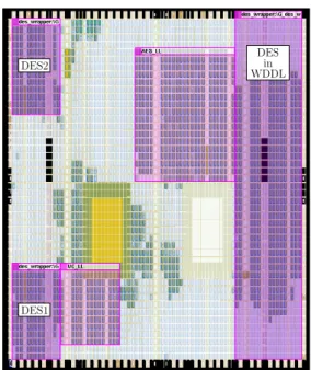
Fig. 1 depicts the floorplan of the SoPC. We can see the unprotected DES1 and DES2 modules on the top left and bottom left corners, which serve as reference to evaluate the security level of the protected ones. The WDDL module, on the right, has been synthesized following the recommenda-tions of Kris Tiri in [19]. The SoPC is programmed in an EP1S25 “Stratix” Altera FPGA (130 nanometers technol-ogy), embedded on a “SHIX2.0”, an 8-layer PCB profes-sional board. Note that this FPGA is not EM-shielded, thus our attack is totally non-invasive.
DES2
DES1
DES in WDDL
Figure 1. Floorplan of the system-on-chip programmed in a Stratix.
4
Experimental Results
4.1
Background Material
Our power analysis sensor drives a “1169A” differential probe from “Agilent Technologies” [1]. The EM field is collected with an antenna of the “HZ-15 Probe Set” from “Rohde and Schwarz” [12], then amplified 60 dB in the frequency range from 100 kHz to 3 GHz. The antenna is mounted on a 2D motorized table and moved over the FPGA through an area of 2.08 cm×2.00 cm. The resolution is of 50 points on X and on Y. In other words, the mechani-cal step equals 400 µm. Fig. 2 is a photograph of the EMA experimental setup, with the antenna over the most leaking point.
The signal outing from the differential probe and the am-plifier are digitized by an “54855 Infiniium Agilent” [1] os-cilloscope, whose bandwidth is 6 GHz and maximal sample rate is 40 GSa/s.
4.2
Spotting by Cartography
As written in the previous section 2.3, we use the fre-quency method described in [13], but we improve it by us-ing no averagus-ing or coherent synchronization signal. In-deed, averaging is powerful to reduce the noise and to dis-cern pattern in a temporal trace, but as the method focuses on a specific frequency, the contribution of the noise on this
Y X Motorized X-Y table ~ H probe FPGA board
Figure 2. The antenna over the “SHIX2.0” board and the FPGA.
latter is minimum because it is spread over the entire fre-quency range. As a consequence, this slightly reduces the number of messages to be intercepted.
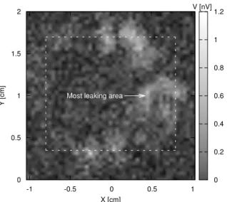
Now, to locate the WDDL DES cryptoprocessor, we have to guess its frequency signature. As explained in Sec-tion 2.2, WDDL runs in two phases: precharge and evalua-tion. In our implementation, these phases occur on the ris-ing edge of the SoPC clock, whose frequency is 8.333 MHz. Therefore, the internal frequency of the WDDL DES cryp-toprocessor can be viewed as being equal to half of that of the SoPC clock, and thus equal to 4.166 MHz. The map for this latter is given in Fig. 3. The dashed rectangle is a land-mark which delimits the ASIC of the FPGA. On the right, the scale gives the voltage dynamic range at the output of the antenna (proportional to the EM field).
Five areas stand out: two at the top, two at the bottom, and one large to the right of the figure. A first validation of our method is that highlighted areas are mostly on the right, which corresponds to the place of the WDDL DES module in the floorplan (refer to Fig. 1). The validation will be completed by analysing the results of the attack on these five points. We detail them in the following section.
4.3
EMA Attack
For all the relevant areas, new acquisitions have been launched to perform a classical EMA, but this time with an external synchronization signal to obtain coherent traces. C/DEMA (C/DPA) has been performed by guessing the value of the R register after the first round of DES, with the Hamming Weight (HW) and Hamming Distance (HD) models, by targeting one to four bit. For clarity of explana-tion, only the best results will be presented in the rest of the
0 0.2 0.4 0.6 0.8 1 1.2 V [nV] -1 -0.5 0 0.5 1 X [cm] 0 0.5 1 1.5 2 Y [cm]
Most leaking area
Figure 3. EM field at 4.333 MHz.
paper. They have been obtained for the large area marked “Most leaking area” in Fig. 3, whose center is located at X=0.416 cm and Y=1 cm. With an eye to illustrate par-ticular phenomenons, a 256 times averaged temporal trace of the EM field at this point is depicted in Fig. 4, on the left. We can observe that the EM field is positive for the precharge, negative for the evaluation. This could be ex-plained by the current inversion of the CMOS capacitors. At the beginning of the precharge phase, the CMOS gates of WDDL go from 1 to 0, whereas this is the other way round when switching from the precharge phase to the evaluation phase.
Tab. 1 reports the statistics for the PA: the number of Measurements To Disclose (MTDs) the key, with the worst value grayed, the SNR and the covariance factor at dis-closure. The SNR indicator illustrates the ratio between the level obtained with the right key and those from the strongest wrong key. For the unprotected DES module, as expected, the best results are obtained with the CPA, by guessing the HD of four bit. For WDDL, because of the precharge, the best results are obtained by guessing the HW (the precharge value of the R register is 0). Targeting a sin-gle bit is more powerful than four bit. Indeed, the leakage in WDDL is caused by the imbalance between the True and the False network, and this imbalance could be opposite for targeted bits, and therefore counterbalance themselves.
Results for the EMA are reported in Tab. 2. Its superior-ity to the C/DPA is well illustrated as the number of MTDs for the unprotected DES module is hundreds of times less.
For WDDL, CEMA able to retrieve the secret key in less than 62,976 encryptions.
By considering the worst MTDs and cross-comparing them, we can conclude that the security gain of our imple-mentation of WDDL equals 7.8 against CPA, 11.6 against CEMA. It confirms that WDDL brings a certain protection against EMA, yet insufficient with respect to the 5,508,224 measurements needed to disclose the key with the CPA.
Finally, Fig. 4 presents on the right the differential trace obtained for the SBox1 after the “CEMA Hamming Weight 1 bit” on the protected module. We can observe correlation on the evaluation phase, but also the opposite correlation on the precharge phase: indeed, the processed data are the same, except that transitions are opposite.
5
Conclusion and Perspectives
We have proposed a method to improve SCAs of DPL countermeasures, and experimentally validated it by suc-cessfully attacking a FPGA-based WDDL DES cryptopro-cessor. This confirms that WDDL with regular place and route shows side-channel leakage, and that differential place and route is mandatory.
Perspectives for future works are first to reiterate the at-tack on a WDDL module with differential place, then dif-ferential place and route, to study the impact on the secu-rity of both improvements. Second, others targets may be attacked such as FPGAs from Xilinx, for which place and route seems to be easier constrainable. Finally, we think that our method can be counteracted if the precharge occurs on the falling edge of the clock: we could imagine combining a DDR architecture [8] that protects against faults attacks by the same token. Alternatively, the precharge can be random, as suggered in [16]. We thus plan to implement and attack these solutions.
References
[1] Agilent Technologies: http://www.agilent.com/.
[2] ´E. Brier, C. Clavier, and F. Olivier. Correlation Power
Anal-ysis with a Leakage Model. Proc. of CHES’04, 3156:16– 29, August 11–13 2004. ISSN: 0302-9743; ISBN: 3-540-22666-4; DOI: 10.1007/b99451; Cambridge, MA, USA. [3] S. Chari, J. Rao, and P. Rohatgi. Template Attacks. In CHES,
volume 2523 of LNCS, pages 13–28. Springer, August 2002.
[4] S. Drimer. Personal web page at Cambridge University,
UK. It is entitled “FPGA design security bibliography”. Available at: http://www.cl.cam.ac.uk/˜sd410/ fpgasec/.
[5] K. Gandolfi, C. Mourtel, and F. Olivier. Electromagnetic
Analysis: Concrete Results. In CHES, volume 2162 of
LNCS, pages 251–261. Springer, May 2001.
[6] B. Gierlichs, L. Batina, and P. Tuyls. Mutual Information Analysis – A Universal Differential Side-Channel Attack. Cryptology ePrint Archive, Report 2007/198, 2007.
[7] S. Guilley, S. Chaudhuri, L. Sauvage, T. Graba, J.-L. Dan-ger, P. Hoogvorst, V.-N. Vong, and M. Nassar. Place-and-Route Impact on the Security of DPL Designs in FPGAs. In
HOST (Hardware Oriented Security and Trust), IEEE, pages 29–35, Anaheim, CA, USA, jun 2008.
[8] P. Maistri and R. Leveugle. Double-data-rate computation as a countermeasure against fault analysis. IEEE Trans.
Com-put., 57(11):1528–1539, 2008.
[9] E. D. Mulder, P. Buysschaert, S. B. ¨Ors, P. Delmotte, B.
Pre-neel, G. Vandenbosch, and I. Verbauwhede. Electromag-netic Analysis Attack on an FPGA Implementation of an Elliptic Curve Cryptosystem. In IEEE International
Confer-ence on Computer as a tool (EUROCON), pages 1879–1882, November 2005. Belgrade, Serbia & Montenegro.
[10] P. Kocher and J. Jaffe and B. Jun. Differential Power Analy-sis. In Proceedings of CRYPTO’99, volume 1666 of LNCS, pages 388–397. Springer-Verlag, 1999. (PDF).
[11] J.-J. Quisquater and D. Samyde. ElectroMagnetic Analysis (EMA): Measures and Counter-Measures for Smard Cards. In I. Attali and T. P. Jensen, editors, Smart Card
Program-ming and Security (E-smart 2001), volume 1240 of LNCS, pages 200–210. Springer-Verlag, 2001. ISSN 0302-9743. [12] Rohde and Schwarz: http://www.rohde-schwarz.
com/.
[13] L. Sauvage, S. Guilley, and Y. Mathieu.
ElectroMag-netic Radiations of FPGAs: High Spatial Resolution
Car-tography and Attack of a Cryptographic Module. ACM,
2008. To be published, full text in http://hal.
archives-ouvertes.fr/hal-00319164/en/. [14] S. P. Skorobogatov. Optically Enhanced Position-Locked
Power Analysis. In CHES, volume 4249 of LNCS, pages 61–75. Springer, 2006.
[15] K. Slattery, J. Neal, and W. Cui. Near-Field Measurements
of VLSI Devices. Electromagnetic Compatibility, IEEE
Transactions on, 41(4):374–384, Nov 1999.
[16] D. Sokolov, J. Murphy, and A. Bystrov. Improving the Secu-rity of Dual-Rail Circuits. In CHES, LNCS, pages 282–297. Springer, Aug 2004.
[17] D. Suzuki and M. Saeki. Security Evaluation of DPA
Coun-termeasures Using Dual-Rail Pre-charge Logic Style. In
CHES, volume 4249 of LNCS, pages 255–269. Springer,
2006. http://dx.doi.org/10.1007/11894063_ 21.
[18] K. Tiri and I. Verbauwhede. A Logic Level Design Method-ology for a Secure DPA Resistant ASIC or FPGA Imple-mentation. In DATE’04, pages 246–251, February 2004. Paris, France.
[19] K. Tiri and I. Verbauwhede. Secure Logic Synthesis. In
FPL, volume 3203 of LNCS, pages 1052–1056, August
2004.
[20] K. Tiri and I. Verbauwhede. A digital design flow for se-cure integrated circuits. IEEE Trans. on CAD of Integrated
Circuits and Systems, 25(7):1197–1208, 2006.
[21] P. Yu and P. Schaumont. Secure FPGA circuits using con-trolled placement and routing. In CODES+ISSS’07:
Pro-ceedings of the 5th IEEE/ACM international conference on Hardware/software codesign and system synthesis, pages 45–50, New York, NY, USA, 2007. ACM.
-40 -30 -20 -10 0 10 20 30 40 50 0 0.2 0.4 0.6 0.8 1 V [nV] t [µs] -40 -30 -20 -10 0 10 20 30 40 0 0.2 0.4 0.6 0.8 1 Covariance factor [%] t [µs] SBox1
Figure 4. EM field at X=0.416 cm and Y=1 cm (left), and covariance factor for the SBox1 (right).
Table 1. Statistics for the Power Analysis.
(a) Unprotected DES Module - CPA Hamming Distance 4 bit
Parameter \ SBox # S1 S2 S3 S4 S5 S6 S7 S8
Measurements To Disclose 478,720 197,056 464,128 614,720 418,944 709,056 348,288 134,080
Covariance factor [%] 5.58 6.23 5.84 4.78 5.42 4.47 4.58 8.23
SNR @ Disclosure 6.22 6.41 6.23 7.03 6.37 5.29 4.57 8.08
(b) WDDL DES Module - CPA Hamming Weight 1 bit
Parameter \ SBox # S1 S2 S3 S4 S5 S6 S7 S8
Measurements To Disclose 5,469,440 1,368,000 557,248 3,597,184 1,116,672 2,876,480 5,508,224 2,563,200
Covariance factor [%] 1.89 0.88 3.27 1.08 2.48 1.75 1.77 1.64
SNR @ Disclosure 3.66 3.79 3.70 4.69 4.80 3.94 4.18 4.63
Table 2. Statistics for the ElectroMagnetic Analysis.
(a) Unprotected DES Module - DEMA Hamming Distance 4 bit
Parameter \ SBox # S1 S2 S3 S4 S5 S6 S7 S8
Measurements To Disclose 2,610 5,422 1,454 4,902 3,056 3,637 2,804 655
SNR @ Disclosure 7.81 6.32 5.65 7.43 7.17 4.69 4.24 7.83
(b) WDDL DES Module - CEMA Hamming Weight 1 bit
Parameter \ SBox # S1 S2 S3 S4 S5 S6 S7 S8
Measurements To Disclose 62,976 32,768 45,312 14,592 27,136 3,840 37,120 27,648
Covariance factor [%] 25.65 28.93 30.25 60.97 37.23 32.16 26.87 44.69