HAL Id: tel-01428037
https://tel.archives-ouvertes.fr/tel-01428037
Submitted on 6 Jan 2017
HAL is a multi-disciplinary open access
archive for the deposit and dissemination of sci-entific research documents, whether they are pub-lished or not. The documents may come from teaching and research institutions in France or abroad, or from public or private research centers.
L’archive ouverte pluridisciplinaire HAL, est destinée au dépôt et à la diffusion de documents scientifiques de niveau recherche, publiés ou non, émanant des établissements d’enseignement et de recherche français ou étrangers, des laboratoires publics ou privés.
Contribution to the study of directive or wide-band
miniature antennas with non-Foster circuits
Abdullah Haskou
To cite this version:
Abdullah Haskou. Contribution to the study of directive or wide-band miniature antennas with non-Foster circuits. Electronics. Université Rennes 1, 2016. English. �NNT : 2016REN1S043�. �tel-01428037�
ANNÉE 2016
THÈSE / UNIVERSITÉ DE RENNES 1
sous le sceau de l’Université Bretagne Loire
pour le grade de
DOCTEUR DE L’UNIVERSITÉ DE RENNES 1
Mention : Traitement de Signal et Télécommunications
Ecole doctorale MATISSE
présentée par
Abdullah Haskou
préparée à l’unité de recherche IETR (UMR 6164)
Institut d’Electronique et de Télécommunications de Rennes
UFR Informatique et Electronique
Contribution à l’Etude
des Antennes Miniatures
Directives ou
Large-Bande avec des Circuits
Non-Foster
Thèse soutenue à Rennes le 7 Septembre 2016 devant le jury composé de :
Robert STARAJ
Professeur à Polytech’Nice Sophia / examinateur et président
Anja SKRIVERVIK
Professeur à l’Ecole Polytechnique Fédérale de Lausanne / rapporteur
Eric RIUS
Professeur à l’Université de Bretagne Occidentale / rapporteur
Christophe DELAVEAUD
Docteur (HDR) au CEA-LETI Grenoble / examina-teur
Sylvain COLLARDEY
Maitre de conférences à l’Université de Rennes 1 / examinateur
Ala SHARAIHA
Professeur à l’Université de Rennes 1 / directeur de thèse
To my parents Ji bo dê û bavê min
Acknowledgments
This thesis started October 1, 2013 and finished September 7, 2016 after three years of hard work, patience, anxiety, and sometimes despair. During these years I had the chance to meet and work with some wonderful people to whom I shall be forever indebted.
First of all I am profoundly grateful for my PhD. advisers Prof. Ala Sharaiha, Dr. Sylvain Collardey and Dr. Dominique Lemur for giving me the opportunity to do this PhD. I am particularly thankful for their guidance, supervision, valuable advise and constant encouragement that helped achieving this work. I am also thankful for our discussions that improved my knowledge.
I would like to thank all the technical staff in Institut d’Electronique et de Télé-communications de Rennes (IETR) for all the prototypes they realized and the measurements they helped me perform.
I am also thankful for all the administrative team in IETR for facilitating my administrative procedures and my professional traveling.
I would also like to give a special thank to all my colleagues for all the interesting time we spent together and the discussions we had.
I would like to express my gratitude to the jury members for the time they de-voted for reading this thesis and their valuable comments and questions that helped enhancing the quality and readability of this manuscript.
Finally, I would like to thank my family for their constant encouragement, support and belief in me. Their presence on my side means the world to me and I shall be forever grateful.
List of Abbreviations
ESA . . . Electrically Small Antenna Q . . . Quality Factor
PCB . . . Printed Circuit Board HPBW . . . Half-Power Beamwidth FBR . . . Front to Back Ratio CP . . . Circularly-Polarized
LHCP . . . Left-Hand Circular Polarization RHCP . . . Right-Hand Circular Polarization NIC . . . Negative Impedance Converter OIP . . . Output Intercept Point
AMC . . . Artificial Magnetic Conductor NF . . . Noise Figure
SNR . . . Signal to Noise Ratio
TCM . . . Theory of Characteristic Modes HIS . . . High Impedance Surface
NII . . . Negative Impedance Inverter OpAmp. . . Operational Amplifier
BJT . . . Bipolar Junction Transistor FET . . . Field Effect Transistor ILA . . . Inverted-L Antenna IIP . . . Input Intercept Point VNA . . . Vector Network Analyzer PSD . . . Power Spectral Density UWB . . . Ultra Wide-Band PCB . . . Printed Circuit Board AUT . . . Antenna Under-Test SLL . . . Side Lobe Level AR . . . Axial Ratio
Contents
Résumé des Travaux 23
General Introduction 27
1 Non-Foster Matched Antennas, Literature Review 33
1.1 Introduction . . . 33 1.2 Foster Theorem . . . 34 1.3 NIC Definition . . . 35 1.4 NIC Applications . . . 37 1.4.1 Antenna Matching . . . 37 1.4.2 Antenna Loading . . . 43 1.4.3 Other Applications . . . 45 1.5 NIC Stability . . . 46 1.6 Conclusion . . . 47
2 Realization of Negative Impedance Convertor (NIC)-Matched An-tennas 49 2.1 Introduction . . . 49 2.2 OpAmp-Based NIC . . . 49 2.3 Transistor-Based NIC . . . 51 2.4 NIC Realization . . . 52 2.4.1 Circuit Topology . . . 52 2.4.2 Parametric Analysis . . . 56 2.4.3 Losses Analysis . . . 59 2.4.4 Stability Analysis . . . 60
2.4.5 Gain Compression Analysis . . . 61
2.4.6 Inter-Modulation Analysis . . . 62
2.4.7 Noise Figure Measurement . . . 64
2.5 NIC-Matched ILA on a PCB . . . 65
2.5.1 Antenna Structure . . . 65
2.5.2 Active Antenna Performance . . . 66
2.5.2.1 Matching Performance . . . 66
2.5.2.2 Stability, Noise and Linearity Performance . . . 67
2.5.2.3 Radiation Performance . . . 68
2.6 NIC-Matched ILA on Small PCB . . . 69
2.6.1 Antenna Structure . . . 69
2.6.2 Active Antenna Performance . . . 70
2.6.2.2 Stability and Noise Performance . . . 71
2.6.2.3 Radiation Performance . . . 72
2.7 Conclusion . . . 73
3 Superdirective Antenna Arrays, Literature Review 75 3.1 Introduction . . . 75 3.2 Optimization Methods . . . 76 3.2.1 Hansen-Woodyard Method . . . 78 3.2.2 Dolph-Chebyshev Method . . . 79 3.2.3 Schelkunoff Method . . . 80 3.2.4 Yaghjian Method . . . 82
3.2.5 Spherical Wave Expansion Method . . . 84
3.2.6 Capon Method . . . 86
3.3 Superdirective Antennas Realizations . . . 87
3.4 Previous Works in IETR . . . 93
3.5 Conclusion . . . 94
4 Design of Parasitic Superdirective Antenna Arrays 97 4.1 Introduction . . . 97
4.2 Superdirective Arrays Limits . . . 97
4.3 Proposed Design Approach . . . 99
4.3.1 Practical Limitations . . . 100 4.3.1.1 Two-Elements Array . . . 101 4.3.1.2 Three-Elements Array . . . 101 4.3.1.3 Four-Elements Array . . . 103 4.3.2 Application on ESAs . . . 104 4.3.2.1 Spiral-Based Array . . . 104
4.3.2.1.1 Integrating a Two-Element Array in a PCB . . . 105
4.3.2.1.2 Measurements Difficulties . . . 109
4.3.2.2 Loop-Based Arrays . . . 114
4.3.2.2.1 Two-Element Array . . . 115
4.3.2.2.2 Two-Element Array on a PCB . . . 119
4.3.2.2.3 Three-Element Array on a PCB . . . 123
4.3.2.3 Folded Monopole-Based Array . . . 126
4.4 Compact Antenna Array Based on Superdirective Elements . . . 131
4.4.1 3D Array Design . . . 131
4.4.1.1 Distance Effect . . . 132
4.4.2 Measurement Results . . . 134
4.5 Planar Arrays Design . . . 135
4.5.1 Unit-Element Description . . . 135
4.5.2 Parasitic Superdirective Unit-Element Design . . . 137
4.5.3 Planar Array Design . . . 139
4.6 CP Array Based on Superdirective Unit-Elements . . . 141
4.7 Conclusion . . . 144
Conclusions and Future Work 147
Publications 153
List of Figures
1 Un organigramme de la méthodologie de conception des réseaux
su-perdirectifs à base d’éléments parasites. . . 25
2 An illustration of an ESA definition. . . 27
3 The bounds on the antenna parameters as a function of ka. (a) Min-imum quality factor, (b) maxMin-imum bandwidth and (c) maxMin-imum di-rectivity. . . 29
4 The bound on the antenna efficiency. (a) Considering Bode-Fano limit on Q and (b) considering Yaghjian-best limit on Q. . . 30
1.1 Passive matching vs. non-Foster matching of a short monopole. . . . 33
1.2 Dipoles bandwidth limits as presented in [20]. (Left) Matching with infinite number of LC and (right) matching with a negative capacitor. 34 1.3 An illustration of different Foster nature components. . . 34
1.4 An illustration of a NIC function. . . 35
1.5 A schematic of the first realized NIC (E1). . . 35
1.6 Linvill balanced NICs. (a) Open circuit stable and (b) short circuit stable. . . 36
1.7 Linvill unbalanced NICs. (a) Open circuit stable and (b) short circuit stable. . . 36
1.8 The catalog of NICs circuits given by Sussman-Fort in [25]. . . 37
1.9 Noise figure improvement as presented by Bahr in [26]. . . 38
1.10 SNR improvement as presented by Sussman-Fort in [27]. . . 38
1.11 The circuit designed by Sussman-Fort Rudisha [28]. (a) Schematic of the circuit and (b) its performance. . . 39
1.12 Antenna input reflection coefficient as presented in [29]. (Left) An-tenna only and (right) anAn-tenna with non-Foster matching circuit. . . 39
1.13 The obtained results by Yifeng et al. in [30]. (a) Input reflection coefficient magnitude and (b) radiation pattern at 200M Hz in E and H plane. . . 40
1.14 The designed NIC in [31]. (Left) A schematic representation and (right) the fabricated prototype. . . 40
1.15 The performance of the antenna presented by White et al. [32]. (a) Schematic and (b) received signal level. . . 41
1.16 The antenna presented by Mirzaei and Eleftheriades in [33]. . . 41
1.17 The proposed antenna in [34]. (a) The antenna geometry, (b) input reflection coefficient magnitude and (c) the realized gain. . . 42
1.18 The proposed antenna in [35]. (a) The antenna geometry, (b) input reflection coefficient magnitude and (c) the realized gain. . . 42
1.19 The proposed active antenna in [36]. (a) The antenna and non-Foster circuit, (b) the measured Q. . . 43 1.20 The circuit designed in [37] S parameters. . . 43 1.21 The performance of the antenna presented by Koulouridis and Stephanopou-los [38]. (a) Schematic and (b) S11. . . 44 1.22 The study presented by Ugarte-Munoz et al. [39]. (a) The
method-ology and (b) the obtained results in terms of the antenna sensitivity to the changes in the NIC parameters. . . 44 1.23 The obtained results in [40]. . . 45 1.24 The studied scenario in [41]. (a) The antenna geometry, (b) input
reflection coefficient magnitude and (c) the radiation pattern. . . 45 1.25 Performance of non-Foster loaded AMC structure presented by
Gre-goire et al. in [42]. (a) AMC unit-cell structure, (b) the non-Foster circuit, (c) the reflection magnitude in dB and (d) the reflection phase. 46 1.26 Performance of HIS structure presented by Long and D. Sievenpiper
in [43]. (a) HIS structure and (b) performance. . . 46 2.1 A schematic of OpAmp-based NIC. . . 50 2.2 The OpAmp test circuit. . . 50 2.3 The measured results of the OpAmp test circuit. (a) Gain and (b)
phase. . . 51 2.4 Schematic of Linvill NIC. (a) A general one and (b) by taking into
account transistor T-model. . . 52 2.5 A schematic of the stabilized NIC in [52]. . . 53 2.6 The regenerated results from [52]. (a) Input reflection coefficient
mag-nitude in dB, (b) input impedance and (c) equivalent capacitance. . . 53 2.7 The initial simulated schematic of the designed circuit. . . 54 2.8 The S parameters magnitude in dB of the initial circuit. (a) Sii and
(b) Sij. . . 54
2.9 The final simulated schematic of the designed circuit. . . 55 2.10 The S parameters magnitude in dB of the final circuit. (a) Sii and
(b) Sij. . . 55
2.11 The effect of the resistance R1 on (a) S11 and (b) S12. . . 56
2.12 The effect of connecting a capacitance Cx in parallel with the
resis-tance R1 on (a) S11 and (b) S12. . . 56
2.13 The effect of biasing on (a) S11 and (b) S12. . . 57
2.14 Calculated stability factors of two-port NIC in simulation. (a) Roulette factor, (b) B and (c) µ. . . . 57 2.15 Two-ports NIC stability circles at (a) 0.11GHz, (b) 0.51GHz (c) 0.91GHz
and (d) 1310MHz. . . 58 2.16 Proposed NIC circuit. (a) General schematic of Linvill floating-type
circuit and (b) a photograph of the prototype. . . 59 2.17 Measured de-embedded parameters of NIC circuit. (a) De-embedded
input impedance and (b) equivalent capacitance. . . 59 2.18 Measured parameters of two-port NIC. (a) Fabricated prototype, (b)
S parameters, (c) losses due to the mismatch and (d) calculated gain. 60 2.19 Calculated stability factors of two-port NIC. (a) Roulette factor, (b)
2.20 Two-ports NIC stability circles at (a) 0.11GHz, (b) 0.51GHz, (c) 0.91GHz and (d) 1.31GHz . . . 61 2.21 The gain compression measurement. (a) Set up and (b) obtained
results. . . 62 2.22 The circuit inter-modulation measurement set up. . . 63 2.23 The circuit inter-modulation measurement results for Pin =−20dBm.
(a) wa− wb, (b) 2wa− wb and (c) 3wa− wb. . . 63
2.24 The circuit inter-modulation measurement results for Pin =−10dBm.
(a) wa− wb, (b) 2wa− wb and (c) 3wa− wb. . . 63
2.25 The circuit inter-modulation measurement results for Pin = 0dBm.
(a) wa− wb, (b) 2wa− wb and (c) 3wa− wb. . . 64
2.26 The circuit NF measurement. (a) The set up and (b) the obtained value in dB. . . . 65 2.27 Passive ILA measured results. (a) Realized prototype, (b) input
re-flection coefficient magnitude in dB, (c) input impedance and (d) required negative capacitor. . . 66 2.28 A photograph of the fabricated active antenna. (a) Top view and (b)
bottom view. . . 67 2.29 Active antenna measured parameters. (a) Fabricated prototype, (b)
input reflection coefficient magnitude in dB, (c) input impedance and (d) Q. . . 67 2.30 The noise floor level of the spectrum analyzer terminated at the
in-put with the non-Foster matched antenna. (a) On (0.01− 3)GHz frequency band and (b) on (0.81− 1.01)GHz frequency band. . . 68 2.31 A comparison between the noise floor levels of the spectrum analyzer
terminated at the input with a matched load and non-Foster matched antenna. . . 68 2.32 The antenna far-field performance. (a) Realized gain and (b) total
efficiency. . . 69 2.33 The active/ passive antenna far-field performance improvement. (a)
realized gain and (b) total efficiency. . . 69 2.34 Passive ILA on a small PCB measured results. (a) Realized prototype,
(b) input reflection coefficient magnitude in dB, (c) input impedance and (d) required negative capacitor. . . 70 2.35 A photograph of the fabricated active antenna on a small PCB. (a)
Top view and (b) bottom view. . . 70 2.36 The measured parameters of the active antenna on a small PCB. (a)
Input reflection coefficient magnitude in dB, (b) input impedance and (d) Q. . . 71 2.37 The noise floor level of the spectrum analyzer terminated at the input
with the non-Foster matched antenna on a small PCB. (a) On (0.01− 3)GHz frequency band and (b) on (0.81− 1.01)GHz frequency band. 72 2.38 A comparison between the noise floor levels of the spectrum analyzer
terminated at the input with a matched load and non-Foster matched antenna on a small PCB. . . 72 2.39 The antenna on a small PCB far-field performance. (a) realized gain
2.40 The active/passive antenna on a small PCB far-field performance im-provement. (a) Realized gain and (b) total efficiency. . . 73 3.1 The directivity improvement of a four 0.2λ spaced dipoles array as
presented by Bloch [76]. . . 76 3.2 The geometry of N-element array along Z-axis. . . 76 3.3 The different parameters of 10-element, 0.25λ-spaced uniform
broad-side array. (a) Excitation coefficients, (b) 2D total directivity radia-tion pattern and (c) 3D total directivity radiaradia-tion pattern. . . 77 3.4 The different parameters of 10-element, 0.25λ-spaced uniform end-fire
array. (a) Excitation coefficients, (b) 2D total directivity radiation pattern and (c) 3D total directivity radiation pattern. . . 78 3.5 The different parameters of 10-element, 0.25λ-spaced Hansen-Woodyard
end-fire array. (a) Excitation coefficients, (b) 2D total directivity ra-diation pattern and (c) 3D total directivity rara-diation pattern. . . 79 3.6 The different parameters of 10-element, 0.25λ-spaced Dolph-Chebyshev
array for R0 = 20dB. (a) Excitation coefficients, (b) 2D total
direc-tivity radiation pattern and (c) 3D total direcdirec-tivity radiation pattern. 80 3.7 The normalized array factor of four-element Schelkunoff array with
nulls at 0o, 90o and 180o for different distances. . . . . 81
3.8 The normalized array factor of Schelkunoff array for nulls at 0o, 90o, a distance of 0.125λ and different number of elements N . . . . 81 3.9 Two d-spaced isotropic array optimal excitation coefficients. (a)
Mag-nitude and (b) phase. . . 82 3.10 Three d-spaced isotropic array optimal excitation coefficients. (a)
Magnitude and (b) phase. . . 83 3.11 Four d-spaced isotropic array optimal excitation coefficients. (a)
Mag-nitude and (b) phase. . . 83 3.12 The performance of N-element d-spaced isotropic array. (a) The
direc-tivity in the main end-fire direction (b) the direcdirec-tivity in the backward en-fire direction and (c) the 2D total directivity radiation pattern for d=0.01 (continuous), d=0.25 (dashed) and d=0.5 (dashed-dotted). . . 84 3.13 The directivity of three-element monopole array as presented by Yaghjian
[82]. . . 84 3.14 The designed arrays in [83]. (a) Geometry and (b) the obtained total
directivity. . . 85 3.15 The proposed parasitic antenna in [85]. (a) The array geometry, (b)
the input reflection coefficient magnitude in dB and (c) the end-fire total directivity and gain as a function of frequency. . . 86 3.16 The tested scenarios and the obtained results in [88]. (a) The array
geometries and (b) the obtained results. . . 87 3.17 The tested scenarios and the obtained results in [89]. (a) The array
geometries and (b) the obtained results. . . 88 3.18 The proposed antenna in [90]. (a) The array geometry and (b) the
ob-tained results (quarter wave monopole (dashed), small Yagi in forward direction (continous) and small Yagi in backward direction (dotted)). 88 3.19 The proposed parasitic antenna in [91]. (a) The array geometry, (b)
3.20 The proposed driven antenna in [92]. (a) The array geometry and (b) the obtained results. . . 89 3.21 The proposed parasitic antenna in [92]. (a) The array geometry and
(b) the gain vs. inter-element spacing. . . 90 3.22 The proposed antenna in [93]. (a) The array geometry and dimensions
and (b) the input reflection coefficient magnitude in dB. . . 90 3.23 The proposed antenna in [93] normalized E-plane and H-plane
co-polar (black) and cross-co-polar (gray) radiation pattern. . . 91 3.24 The proposed parasitic antenna in [94]. (a) The array geometry and
(b) the obtained results. . . 91 3.25 The proposed antenna in [96]. (a) The array geometry and (b) the
obtained results. . . 92 3.26 The proposed parasitic antenna in [97]. (a) The array geometry, (b)
the reactance of the optimal loads associated to the parasitic elements, and (c) the simulated maximum directivity as a function of frequency. 92 3.27 Optimized backscattering cross-section of N isotripic elements as a
function of the elmenet separation [98]. . . 93 3.28 The directivity of a three-dipole array vs. spacing as reported in [99]. 93 3.29 The proposed parasitic antenna in [100]. (a) The array geometry, (b)
the total directivity as a function of the spacing and (c) the 3D total directivity radiation pattern for d=3mm. . . 94 3.30 The proposed parasitic antenna in [102]. (a) The array geometry and
dimensions, (b) the input reflection coefficient magnitude in dB, (c) the end-fire total directivity as a function of frequency and (c) the 3D total directivity radiation pattern at the design frequency. . . 94 4.1 The calculated parameters of N-element d-spaced isotropic
superdi-rective array. (a) End-fire total directivity and (b) normalized trans-mitted power. . . 98 4.2 The effect of the error in the coefficients estimation on the directivity
of N-element, d-spaced isotropic array. (a) N=2, (b) N=3 and (c) N=4. 98 4.3 A flow chart of the proposed design methodology. . . 99 4.4 Two-dipole array simulated total end-fire directivity. (a) Exciting the
different elements and (b) exciting the second element and neglecting the negative resistances. . . 101 4.5 Three-dipole array calculated excitation coefficients. (a) Magnitude
and (b) phase. . . 102 4.6 Three-dipole array calculated required loads. (a) Resistance and (b)
reactance. . . 102 4.7 Three-dipole array simulated total end-fire directivity. (a) Exciting
the different elements and (b) exciting the second element and ne-glecting the negative resistances. . . 103 4.8 Four-dipole array simulated total end-fire directivity. (a) Exciting the
different elements and (b) exciting the second element and neglecting the negative resistances. . . 103 4.9 Simulated parameters of the different arrays when exciting the
sec-ond element and neglecting the negative resistances. (a) radiation efficiency and (b) total gain in dB. . . 104
4.10 Miniaturized spiral antenna. (a) Antenna geometry and dimensions, (b) simulated input reflection coefficient magnitude in DB and (c) simulated 3D total directivity radiation pattern. . . 105 4.11 Reference array. (a) Geometry, corresponding dimensions and surface
current distribution and (b) simulated 3D directivity radiation patterns.105 4.12 Scenario one. (a) Geometry and surface current distribution and (b)
simulated 3D directivity radiation patterns. . . 106 4.13 Scenario two. (a) Geometry and surface current distribution and (b)
simulated 3D directivity radiation patterns. . . 107 4.14 Scenario three. (a) Geometry and surface current distribution and
(b) simulated 3D directivity radiation patterns. . . 108 4.15 The slot size effect on the array performance. (a) Maximum
directiv-ity and radiation efficiency and (b) input reflection coefficient. . . 109 4.16 Feeding scenario one. (a) Geometry and surface current distribution
and (b) simulated 3D directivity radiation patterns. . . 110 4.17 Feeding scenario two. (a) Geometry and surface current distribution
and (b) simulated 3D directivity radiation patterns. . . 110 4.18 Feeding scenario three. (a) Geometry and surface current distribution
and (b) simulated 3D directivity radiation patterns. . . 111 4.19 Feeding scenario four. (a) Geometry and surface current distribution
and (b) simulated 3D directivity radiation patterns. . . 111 4.20 Simulated input reflection coefficient magnitude for all scenarios. . . . 112 4.21 Simulated 2D total directivity radiation pattern for all scenarios. (a)
Horizontal plane and (b) vertical plane. . . 112 4.22 Photographs of the fabricated prototypes. (a) Scenarios one, (b)
sce-narios two and (c) scesce-narios three. . . 112 4.23 Measured input reflection coefficient magnitude for different scenarios. 113 4.24 Measured 2D total directivity radiation pattern for different scenarios.
(a) Horizontal plane and (b) vertical plane. . . 113 4.25 Measured 3D total directivity radiation patterns for different
scenar-ios. (a) Scenario one, (b) scenario three and (c) scenario four. . . 114 4.26 The miniaturized unit-element. (a) Geometry and dimensions, (b)
simulated input reflection coefficient magnitude and (c) simulated 3D total directivity radiation pattern. . . 115 4.27 Two-element array. (a) Geometry and dimensions and (b) simulated
input reflection coefficient magnitude. . . 115 4.28 Two-element array’s simulated 3D total directivity radiation pattern.
(a) Fully-driven array and (b) parasitic one. . . 116 4.29 Two-element array’s simulated 2D total directivity radiation patterns.
(a) Horizontal plane and (b) vertical plane. . . 116 4.30 Parasitic two-element array’s simulated input reflection coefficient
magnitude and end-fire total directivity. . . 117 4.31 Two-element array’s simulated surface current distribution.(a)
Fully-driven array and (b) parasitic one. . . 117 4.32 Two-element array simulation with (a) a horizontal coaxial cable and
(b) a vertical one. . . 118 4.33 Two-element array simulated S11 in dB with an excitation cable. . . . 118
4.34 Two-element array simulated 3D total directivity radiation pattern at the design frequency with (a) a horizontal coaxial cable and (b) a vertical one. . . 118 4.35 Two-element array mounted on a PCB. (a) Geometry and dimensions
and (b) simulated input reflection coefficient magnitude. . . 119 4.36 Two-element array mounted on a PCB’s simulated 3D total directivity
radiation pattern. (a) Fully-driven array and (b) parasitic one. . . 120 4.37 Two-element array mounted on a PCB’s simulated 2D total directivity
radiation patterns. (a) Horizontal plane and (b) vertical plane. . . 120 4.38 Parasitic two-element array mounted on a PCB’s simulated input
re-flection coefficient magnitude and end-fire total directivity. . . 121 4.39 Two-element array mounted on a PCB’s simulated surface current
distribution.(a) Fully-driven array and (b) parasitic one. . . 121 4.40 Two-element array mounted on a PCB. (a) A photograph of the
pro-totype, (b) measured input reflection coefficient magnitude and (c) measured 3D total directivity radiation pattern. . . 122 4.41 Two-element array mounted on a PCB’s measured 2D total directivity
radiation patterns. (a) Horizontal plane and (b) vertical plane. . . 122 4.42 Two-element array mounted on a PCB’s measured parameters. (a)
Maximum total directivity and (b) efficiency. . . 123 4.43 Three-element array mounted on a PCB. (a) Geometry and
dimen-sions and (b) simulated input reflection coefficient magnitude. . . 123 4.44 Three-element array mounted on a PCB’s simulated 3D total
direc-tivity radiation pattern. (a) Fully-driven array and (b) parasitic one. 124 4.45 Three-element array mounted on a PCB’s simulated 2D total
direc-tivity radiation patterns. (a) Horizontal plane and (b) vertical plane. 124 4.46 Parasitic three-element array mounted on a PCB’s simulated input
reflection coefficient magnitude and end-fire total directivity. . . 125 4.47 Three-element array mounted on a PCB’s simulated surface current
distribution.(a) Fully-driven array and (b) parasitic one. . . 125 4.48 Three-element array mounted on a PCB’s experimental results. (a)
Fabricated prototype, (b) input reflection coefficient magnitude in dB and (c) 3D total directivity radiation pattern at the resonance frequency (903MHz). . . 126 4.49 Three-element array mounted on a PCB’s measured 2D total
direc-tivity radiation patterns at the resonance frequency (903MHz). (a) Horizontal plane and (b) vertical plane. . . 126 4.50 The unit-element. (a) Geometry and dimensions and (b) simulated
3D total directivity radiation pattern. . . 127 4.51 The surface current distribution in (a) fully-driven array and (b)
par-asitic array. . . 128 4.52 Parasitic array simulated and measured parameters. (a) A
photo-graph of the realized prototype, (b) input reflection coefficient mag-nitude in dB, (c) maximum total directivity and (d) radiation efficiency.129 4.53 Proposed array 3D total directivity radiation pattern. (a) Simulated
driven, (b) simulated parasitic and (c) measured parasitic. . . 129 4.54 Proposed array simulated and measured 2D total directivity radiation
4.55 Parasitic array 3D co-polar directivity radiation pattern. (a) Simu-lated and (b) measured. . . 130 4.56 Parasitic array 3D cross-polar directivity radiation pattern. (a)
Sim-ulated and (b) measured. . . 131 4.57 Broadside array geometry and simulated parameters. (a) Geometry
and dimensions, and (b) 3D total directivity radiation pattern. . . 132 4.58 Broadside array simulated parameters. (a) input reflection coefficient
magnitude in dB and broadside directivity and (b) mutual coupling magnitude in dB. . . 132 4.59 Broadside array simulated parameters as a function of the distance.
(a) Input reflection coefficient magnitude in dB and (b) total direc-tivity and radiation efficiency. . . 133 4.60 Broadside array simulated 2D total directivity radiation patterns as
a function of the distance. (a) Horizontal plane and (b) vertical plane. 133 4.61 Broadside array prototype and measured results. (a) Fabricated
pro-totype, (b) 3D total directivity radiation pattern and (c) input reflec-tion coefficient magnitude in dB and maximum total directivity. . . . 134 4.62 Broadside array measured 2D total directivity radiation pattern.(a)
Horizontal plane and (b) vertical plane. . . 135 4.63 The unit-element simulated and measured parameters. (a) Geometry
and dimensions, (b) fabricated prototype, (c) input reflection coeffi-cient magnitude in dB, (d) surface current distribution and (e) 3D total directivity radiation pattern. . . 136 4.64 The unit-element simulated and measured 2D total directivity
radia-tion pattern. (a) E plane and (b) H plane. . . 136 4.65 Parasitic two-element array parameters as a function of the
inter-element distance. (a) Simulated input reflection coefficient magnitude in dB, (b) required resistance, (c) required reactance, (d) obtained total directivity, and (e) obtained radiation efficiency. . . 137 4.66 Two-element array with 2.5cm spacing simulated and measured
pa-rameters. (a) Geometry and dimensions, (b) fabricated prototype, (c) input reflection coefficient magnitude in dB, (d) surface current distribution and (e) 3D total directivity radiation pattern. . . 138 4.67 Two-element array with 2.5cm spacing simulated and measured 2D
total directivity radiation pattern. (a) E plane and (b) H plane. . . . 139 4.68 Planar array simulated and measured parameters as a function of
the separation. (a) Geometry, (b) fabricated prototype, (c) mutual coupling, (d) input reflection coefficient magnitude in dB, (e) total directivity and (f) radiation efficiency. . . 140 4.69 Planar array 3D total directivity radiation pattern for d=26cm. (a)
Simulated and (b) measured. . . 140 4.70 Planar array 2D total directivity radiation pattern for d=26cm. (a)
E plane and (b) H plane. . . 141 4.71 Planar CP array simulated parameters as a function of the separation.
(a) Geometry, (b) LHCP directivity and radiation efficiency and (c) HPBW and CP aperture. . . 142
4.72 Planar CP array with d = 15.6cm. (a) Fabricated prototype, (b) input reflection coefficient magnitude in dB, (c) measured LHCP di-rectivity and AR as a function of the frequency and (d) AR. . . 143 4.73 Planar CP array 3D directivity radiation pattern for d=15.6cm. (a)
Co-polar and (b) cross-polar. . . 143 4.74 Planar CP array 2D LHCP and RHCP directivity radiation pattern
for d=15.6cm. (a) E plane and (b) H plane. . . 144 4.75 The obtained directivity of different designed antennas. . . 145 4.76 Proposed three-element array simulated parameters as a function of
the inter-element distance. (a) Array geometry, (b) input reflection coefficient magnitude in dB, (c) total directivity and (d) radiation efficiency. . . 149 4.77 Three-element array with 6cm spacing simulated and measured
pa-rameters. (a) Fabricated prototype, (b) input reflection coefficient magnitude in dB and (c) 3D total directivity radiation pattern. . . . 150 4.78 Three-element array with 6cm spacing simulated and measured
pa-rameters 2D total directivity radiation patterns. (a) E-plane, (b) H-plane. . . 150 4.79 Planar array based on a tree-element antenna simulated as a function
List of Tables
4.1 A summary of the simulated obtained results for different PCB inte-gration configurations. . . 108 4.2 A summary of the simulated and measured results of different coaxial
cable connection configurations. . . 114 4.3 The calculated excitation coefficients, the equivalent- and the
applied-loads for four-element array. . . 127 4.4 A summary of all the designed antennas. . . 146
Résumé des Travaux
Contexte de L’Etude
Avec l’évolution des technologies sans fil, un smartphone doit supporter de plus en plus de standards de communication (GSM, UMTS, LTE, Bluetooth, WiFi, GPS, ...) afin d’offrir aux usagers les meilleures performances possibles. De plus, de nouvelles applications comme les systèmes de pointage (télécommande radio) peu-vent nécessiter l’intégration de systèmes compacts à rayonnement directifs néces-saires pour contrôler séparément plusieurs périphériques en fonction de l’orientation de la télécommande. Ces besoins nécessitent un effort de plus en plus important d’intégration des systèmes et donc des antennes dont la miniaturisation doit per-mettre conserver des performances acceptables en termes de bande passante, de directivité et d’efficacité. Cependant, les performances des antennes ont des limites fondamentales liées à leurs dimensions physiques. Plusieurs études ont précisé les limites fondamentales pour des Antennes Électriquement Petites (AEP). En 1947, A.H. Wheeler a été le premier à étudier ces limites. Il a défini une AEP comme une antenne avec ka < 1, où k = 2πλ est le nombre d’onde, λ est la longueur d’onde en espace libre et a est le rayon de la plus petite sphère entourant l’antenne. Chu a montré que le facteur de qualité (Q) d’une antenne est inversement proportionnel à (ka)3 ce qui signifie que la miniaturisation augmente de manière significative le
facteur Q. De plus, Bode-Fano et Yaghjian-Best ont montré que la bande passante d’une antenne est inversement proportionnelle à son facteur de qualité. Par con-séquent, il est difficile de concevoir des AEP à large bande de fréquence. Harrington a démontré que la directivité d’une antenne est aussi directement reliée à ses di-mensions et qu’en raison de cette contrainte, il est difficile de concevoir des AEP directives.
Les Contributions de la Thèse
Bien que les limites définies par Bode-Fano et Yaghjian-Best, concernant la bande passante des antennes, ne sont applicables qu’aux antennes adaptées par des circuits de type Foster, des circuits dits non-Foster semblent en mesure de surpasser ces lim-ites. De plus, la théorie sur les réseaux superdirectifs montre que la limite de Harring-ton sur la directivité des antennes peut être dépassée dans certaines conditions. Par conséquent, ce travail se concentre sur l’étude et la conception d’antennes adaptées par des circuits à comportement non-Foster et de réseaux d’antennes superdirectifs comme solutions possibles pour l’amélioration des performances des AEP.
Les Antennes Adaptées par des Circuits Non-Foster
La première partie de cette thèse a été menée dans le cadre du projet ANR "Sys-tèmes d’antenne capteur miniature (SENSAS)". Ce projet a pour but d’étudier, de réaliser et de caractériser de nouvelles antennes ultra-miniatures et intelligentes, capables de s’adapter à leur environnement et, pour certaines d’entre elles, intégrant des capteurs de température ou de pression. Le projet associe les compétences de trois laboratoires de recherche CEA-Leti, l’IETR et LEAT, et de deux entreprises, Technicolor et SENSeOR [1]. Dans ce cadre, un convertisseur d’impédance négative (NIC) de type Linvill flottant à comportement non-Foster a été réalisé pour obtenir un condensateur de faible valeur (quelques pF) mais négative, donc de valeur de réactance très élevée. Dans la bande UHF, les capacités parasites des transistors sont exploitées afin d’atteindre ces faibles valeurs de capacité. Un prototype du cir-cuit à deux ports est réalisé pour étudier les pertes du circir-cuit ainsi que sa stabilité. Les résultats obtenus montrent que le circuit présente un gain satisfaisant en basse fréquence (7dB autour de 250M Hz). Avec la fréquence, le gain du circuit diminue dans la bande utile (autour de 910M Hz) pour atteindre 1dB. A partir de 1.3GHz, le circuit commence à générer des pertes qui augmentent alors avec la fréquence (8dB à 3GHz). Ce prototype est aussi utilisé pour analyser la stabilité du circuit selon différents critères. Les résultats obtenus montrent que le circuit est inconditionnelle-ment stable à partir de 1.61GHz. Les cercles de stabilité du circuit sont tracées dans la bande d’instabilité et montrent qu’une charge capacitive (ce qui est le cas avec une antenne de type dipôle) stabilisera le circuit. Les produits d’intermodulation du circuit sont également mesurés et mettent en évidence des points d’interceptions en sortie (OIP) du deuxième et troisième ordre assez élevés. Le point de compression du gain du circuit est aussi étudié et montre que le circuit présentent des points de compression et de saturation très élevés (12.5dBm et 27.5dBm respectivement). Une fois le circuit caractérisé, celui-ci est utilisé pour adapter une antenne miniature de type ILA (Inverted L-Antenna) dans la bande de fréquence (0.76−2.17GHz). La stabilité de l’antenne associée au circuit est mise en évidence à l’aide d’un analyseur de spectre. De plus, une comparaison entre le niveau de bruit de l’analyseur de spectre, connecté à l’antenne ou à une charge adaptée (50Ω), montre que le circuit n’ajoute pratiquement aucun bruit. Les résultats de mesures montrent aussi que l’antenne présente une bonne linéarité avec un rendement total acceptable (envi-ron 20%). Les caractéristiques de rayonnement sont mesurées suivant deux modes de fonctionnement, en émission et en réception, montrant ainsi que l’antenne fonc-tionne de façon réciproque. Le rendement est semblable dans les deux modes. En prolongement de ces travaux, le circuit NIC est également utilisé pour adapter une antenne ILA de mêmes dimensions que la précédente mais intégrée sur un PCB plus petit (équivalent à une clef USB). Cette antenne présente une oscillation en basse fréquence (autour de 100M Hz) mais aucune harmonique secondaire n’est mise en évidence en haute fréquence. En termes de bande-passante et rayonnement, cette antenne est aussi performante que la première sur le plus grand PCB.
Réseaux d’Antennes Superdirectifs
La deuxième partie de cette thèse s’inscrit dans le cadre du projet "Super-directivité pour le contrôle du rayonnement des objets communicants (SOCRATE)" financé
également par l’Agence Nationale de la Recherche (ANR). Ce projet regroupe des équipes de recherche du CEA-Leti et de l’IETR, ainsi que deux partenaires indus-triels (Movea et Tagsys) portant des applications demandeuses en antennes com-pactes et directives. Le but du projet et d’améliorer la directivité des antennes électriquement petites [2]. Dans ce contexte, les limites théoriques des réseaux d’antennes superdirectifs ont tout d’abord été mises en évidence à partir d’un état de l’art exhaustif. Suite à cette première phase, une approche simple et pratique a été développée afin de faciliter la conception des réseaux d’antennes superdirectifs à base d’éléments parasites (ou chargées). La méthode consiste à intégrer les diagrammes de rayonnement des éléments du réseau dans les équations de Yaghjian pour calculer les pondérations en courant qui maximise la directivité du réseau dans la direction end-fire. Les pondérations obtenues et la matrice Z du réseau sont ensuite utilisées pour calculer les impédances actives de chaque élément. Finalement, un élément du réseau est choisi pour être alimenté tandis que les autres sont connectés à des charges équivalentes à leurs impédances actives. Les différentes étapes de la méthode sont décrites sur la Figure 1.
Figure 1: Un organigramme de la méthodologie de conception des réseaux superdirectifs à base d’éléments parasites.
Les limites pratiques de l’approche proposée sont démontrées par une étude paramétrique sur des réseaux à base de dipôles. Cette analyse montre que la méth-ode utilisant des charges n’est pas limitée par le nombre des éléments, ni par la distance inter-élément. Cette analyse montre également qu’en raison des limites et des difficultés pratiques, la conception de réseaux superdirectifs est effectuée suiv-ant un compromis entre directivité, efficacité de rayonnement et dimension (nombre d’éléments et espacement inter-éléments). L’approche proposée est également util-isée pour la conception de réseaux superdirectifs à deux, trois et quatre éléments à base d’AEP. Dans tous les cas, la distribution des courants à la surface des antennes, notamment des éléments parasites, est très proche de celle du réseau qui aurait tous ses éléments alimentés. La même comparaison entre réseau alimenté et réseau par-asite peut être faite concernant l’allure des diagrammes de rayonnement ainsi que de la valeur de directivité totale. En outre, la directivité end-fire du réseau parasite est maximale à la fréquence de conception pour laquelle les charges sont calculées.
Les résultats mesurés pour tous les prototypes fabriqués valident complètement les résultats de simulation. Ces travaux sur la superdirectivité d’antennes planaires ont aussi permis de répondre aux problématiques d’intégration sur PCB ainsi que de car-actérisation expérimentale. Il a été montré que le phénomène de superdirectivité est très sensible à l’environnement. Cette problématique a nécessité de mener une étude afin d’optimiser l’intégration des antennes superdirectives sur des circuits imprimés (PCB) afin de conserver leurs directivités. Pour quelques exemples d’antennes, les résultats obtenus à partir de cette étude montrent que la configuration du PCB, cest-à-dire la position du réseau, a un impact significatif sur la directivité et l’efficacité de rayonnement. Ajouter une fente sur le PCB permet de contrôler la distribution du courant afin de maintenir une contribution constructive et ainsi de conserver, non seulement, la superdirectivité de l’antenne mais aussi d’accroître son efficac-ité. Confronté à des difficultés de mesure des AEP superdirectives intégrées sur PCB, différents scénarios pour connecter le système d’alimentation à l’antenne ont été évalués. Les résultats obtenus montrent qu’une connexion correcte du système d’excitation peut réduire ces effets négatifs, et par conséquent, permettre la carac-térisation de l’antenne. La dernière partie de ces travaux a permis de développer une nouvelle stratégie pour concevoir des réseaux compacts utilisant des éléments superdirectifs dans la bande UHF RFID (866M Hz). Un premier design de réseau 3D dont les dimensions totales sont de 20×20×7cm3(0.58λ×0.58λ×0.2λ) a permis d’atteindre une directivité totale de 11.4dBi avec une efficacité de rayonnement de 73%. Les ouvertures angulaires à mi-puissance (HPBW) dans les plans horizontal et vertical atteignent respectivement 56o et 48o pour un rapport avant-arrière (Front
to Back Ratio, FBR) de 13.2dB. Les résultats simulés et mesurés sont en très bon accord. À directivité égale, ce réseau est nettement plus compact que d’autres an-tennes plus classiques (Yagi par exemple). Ce travail basé sur un réseau à deux éléments peut être généralisé pour des réseaux à N-éléments superdirectifs tout en gardant à l’esprit les compromis à faire entre dimensions, directivité et efficacité de rayonnement du réseau. Un second réseau planaire a été développé à partir d’une antenne superdirective à deux éléments superposés. Cet élément superdirectif, de dimensions 8× 8 × 2.5cm3(0.23λ× 0.23λ × 0.07λ) dans la bande UHF RFID, atteint
une directivité totale de 7dBi et une efficacité de rayonnement de 43.4%. Ce élé-ment compact et superdirectif est ensuite intégré dans le réseau planaire de 2× 2. Pour une distance inter-élément de 26cm(0.75λ) et pour des dimensions totales de
34× 34 × 2.5cm3(0.98λ× 0.98λ × 0.07λ), une directivité totale de 12.6dBi et une
efficacité de rayonnement de 41% sont obtenues. Cette antenne est significativement plus petite que des réseaux classiques ayant la même directivité. Enfin, ce réseau planaire est aussi développé pour fonctionner en polarisation circulaire (CP). Les dimensions totales du réseau sont de 22× 22 × 2.5cm3(0.63λ× 0.63λ × 0.07λ). Ce
dernier présente une directivité main gauche (LH) de 10.3dBic et un rendement de rayonnement de 38.5%.
La Valorisation des Résultats
Les travaux menés dans le cadre de cette thèse ont été valorisés par 5 revues, 14 communications dans des conférences internationales, 2 communications dans une conférence nationale et 3 communications dans des journées thématiques nationales.
General Introduction
Background
Many emerging radio technologies require supporting multiple communications stan-dards. For example a smart phone requires supporting GSM, UMTS, LTE, Blue-tooth, WiFi, GPS,...etc. standards. In other applications, as a universal remote control, a small and directive antenna is required to separately control multiple de-vices depending on the remote orientation. This requires a significant effort on the antenna miniaturization while keeping an acceptable performance (in terms of band-width, directivity and efficiency). However, the antenna performance is limited with some fundamental limits related to its physical dimensions. Multiple researchers addressed the fundamental limits of Electrically Small Antennas (ESAs) [3]-[18]. A. H. Wheeler was the first to address these limits [3, 4]. He defined an ESA as an antenna with ka < 1 as shown in Figure 2, where k = 2πλ is the wave number, λ is the free space wavelength and a is the radius of the smallest sphere enclosing the antenna.
Figure 2: An illustration of an ESA definition.
The first relationship between the antenna size and its Quality Factor (Q) was presented by Chu [5] in 1948. Based on the approximations indicated by Chu this limit is given by [6]:
Qmin =
1 + 2(ka)2
(ka)3(1 + (ka)2) (1)
However, this limit was later refined by McLean in 1996 [6]. He expressed the minimum Q of a linear ESA in free space as:
Qmin =
1 (ka)3 +
1
(ka) (2)
For very small antennas, this limit can be approximated as follows:
Qmin ≈
1
As it can be noticed, the antenna Q is inversely proportional to the third power of its size factor meaning that miniaturizing the antenna will significantly increase its Q. The minimum Q of a Circularly-Polarized (CP) ESA is given by:
Qmin = 1 2 ( 1 (ka)3 + 2 (ka) ) (4) Figure 3(a) shows both Chu and McLean bound on an antenna Q as function of ka. As it can be noticed, both limits are in a very good agreement for small dimensions. However, as the antenna dimensions increases the divergence between the two limits also increases. Bode and Fano derived a bound on the antenna fractional matching bandwidth based on its Q [7]. The limit was derived for a shunt (parallel) RC load. Bode showed that the fundamental limitation on the matching network is:
ˆ ∞ 0 ln( 1 |Γ|)dw6 π RC (5)
where |Γ| is the reflection coefficient magnitude. If |Γ| is kept to |Γm| inside the
radial frequency band w and to unity outside this band, this limit can be written as:
w ln( 1
|Γm|
)6 π
RC (6)
Or equivalently, the fractional bandwidth Bw = ww
0 can be given in terms of the
load quality factor Q = w0RC as:
Bw6 π
Q ln(|Γ1
m|)
(7) Yaghjian and Best derived a similar bound for general single-feed (one-port) lossy or lossless linear antenna tuned to resonance or unti-resonance given by:
Bw = S− 1
Q√S (8)
where S is the standing wave ratio and it is related to Γm as:
S = 1 +|Γm|
1− |Γm|
(9) Figure 3(b) shows Bode-Fano and Yaghjian-Best limits on antenna S11 < −10dB
bandwidth as a function of ka. It can be noticed that the two limits are in a good agreement for small ka (< 0.5) and as ka increases the difference between them increases. In general, due to the assumptions under-which Fano limit was derived, this limit is more optimistic than Yaghjian’s one. Due to this fundamental limit, it is hard to design wide-band small antennas.
As for the antenna directivity, Harrington derived an upper bound depending on the spherical wave order N associated to the antenna radiation given by:
Dmax= N2+ 2N (10)
Harrington also provided a relationship between the antenna size and the spherical wave order given by:
However, Harrington limit was derived considering lossless antennas, hence in the case of ESAs with ka < 0.5 it yields negative directivity in dBi. Furthermore, it does not converge to the directivity of Huygens source. Consequently, in [19], the authors proposed a renormalization of the second part of this limit (the spherical wave order) to fulfill the directivity definition and the physical behavior of ESAs. The renormalized spherical wave order is given by:
N = k(a + λ
2π )
(12) Figure 3(c) shows Harrington limit on the antenna directivity and the renormalized limit as a function of ka. Due to this fundamental limit, it is hard to design directive small antennas. 0 0.5 1 1.5 2 10−1 100 101 102 ka Qmin Chu McLean (a) 0 0.5 1 1.5 2 0 1 2 3 4 5 ka Bw max Bode−Fano Yaghjian−Best (b) 0 0.5 1 1.5 0 5 10 15 ka Dmax [dBi] Harrington Renormalized (c)
Figure 3: The bounds on the antenna parameters as a function of ka. (a) Minimum quality factor, (b) maximum bandwidth and (c) maximum directivity.
Now assuming a lossy antenna with a radiation efficiency of ηrad, MacLean
min-imum quality factor can be modified as follows:
Qmin = ηrad ( 1 (ka)3 + 1 (ka) ) (13) Replacing the value of Q in the bound on the antenna bandwidth given by Bode-Fano, the following bound on the antenna efficiency can be derived:
ηrad = π(ka)3 Bw ln(|Γ1 m|) ( (ka)2+ 1) (14)
and by changing the value of Q in the bound on the antenna bandwidth given by Yaghjian-Best, the following bound on the antenna efficiency can be derived:
ηrad =
(S− 1)(ka)3
√
S Bw ((ka)2+ 1) (15)
As it can be noticed, the antenna bandwidth is inversely proportional to the antenna relative bandwidth while it is proportional to the third power of its size factor. This means that, for a fixed dimension, there is a trade-off between the antenna bandwidth and its efficiency. Figure 4 shows the limit on antenna efficiency for different relative bandwidths. Since Fano’s limit is more optimistic concerning the obtainable bandwidth, it is also more optimistic concerning the attainable efficiency.
0 0.2 0.4 0.6 0.8 1 0 0.2 0.4 0.6 0.8 1 ka ηrad Bw=5% Bw=15% Bw=25% Bw=35% (a) 0 0.2 0.4 0.6 0.8 1 0 0.2 0.4 0.6 0.8 1 ka ηrad Bw=5% Bw=15% Bw=25% Bw=35% (b)
Figure 4: The bound on the antenna efficiency. (a) Considering Bode-Fano limit on Q and (b) considering Yaghjian-best limit on Q.
Objectives
In the previous section it was shown that the antenna performance (in terms of band-width, directivity and efficiency) is limited by the fundamental limits related to its dimensions. This work is done in the framework of two French National Research Agency (ANR) Projects. The first project, systèmes d’antenne capteur miniature "SENSAS", aims to study, implement and characterize new ultra-miniature and smart antennas, that are able to adapt to their changing environment, and for some of them, including detection capabilities. The project combines the expertise of three research laboratories CEA-Leti, IETR and LEAT, and two companies, Tech-nicolor and SENSeOR [1]. The second project, super-directivité pOur le Contrôle du Rayonnement des objets communicants, aimes to improve the directivity of ESAs. It brings together research teams from CEA-Leti and IETR and two industrial part-ners (Movea and TAGSYS) [2]. In this context, the main objective of this thesis is the design of ESAs approaching, or exceeding, the well known fundamental limits on antenna bandwidth and directivity.
Layout
This thesis is organized in four chapters.
In the first chapter, a the definition of non-Foster circuits is presented. A litera-ture review on the different aspect and applications of non-Foster circuits is given showing that using this kind of circuits can help designing ESAs overcoming the theoretical limits on Q and bandwidth.
In the second chapter, a non-Foster circuit is designed and characterized in terms of losses, stability, linearity and inter-modulation. Then, the circuit is ued to match to ILAs showing a significantly wide-band, stable, low-noise performance.
In the third chapter, superdirective arrays are defined and their different optimiza-tion methods are presented. The state of the art on this kind of arrays is summarized showing that in some parasitic arrays a frequency optimization is required while in others resistive loads are applied which highly reduces the antenna efficiency. In the fourth chapter, a design approach for parasitic superdirective antenna arrays is presented. A parametric analysis on dipole-based arrays is performed to investigate
the practical limitations. The method is later used to design multiple superdirec-tive ESA-based arrays surpassing Harrington’s limit on antenna directivity. Then, the integration of superdirective ESAs in PCBs is investigated via different scenar-ios. Next, measuring superdirective ESAs integrated in PCBs is also investigated via different feeding configurations. Later, a new strategy is presented to obtain a 3D small-size broadside array using compact end-fire unit-elements for UHF band. Afterward, a two-element parasitic superdirective antenna array is designed and in-tegrated in a compact 2× 2 planar antenna array. Finally, a compact CP planar array for 866M Hz band based on superdirective arrays is presented.
Chapter 1
Non-Foster Matched Antennas,
Literature Review
1.1
Introduction
We previously mentioned Bode-Fano fundamental limit on the antenna bandwidth when a passive matching circuit is used. One solution to surpass this limit is using a non-Foster matching circuit. Let us consider the example of a small monopole that can be modeled as a resistor in series with a capacitance (for example 1pF ). To eliminate this antenna’s reactance, it can be connected in series with an inductor (passive matching) or a negative capacitor (non-Foster matching). While the first solution eliminates the antenna’s reactance at a single frequency, the second does that for the whole band and therefore has a much wider bandwidth (see Figure 1.1).
Figure 1.1: Passive matching vs. non-Foster matching of a short monopole.
Hirvonen et al. presented the bandwidth limitations for dipoles matched with negative impedances [20]. It was shown that even though in reality infinite band-widths cannot be achieved, the bandwidth achieved with one negative capacitor demonstrates a larger than the ones obtained when tuning with infinite passive components. Figure 1.2 shows that, for example, for an antenna with ka = 0.4, the achieved bandwidth for V SW R = 1.5 is 15% using infinite passive tuning while it is 24% using a negative capacitor. The "non-Foster" notation comes from Foster
theorem.
Figure 1.2: Dipoles bandwidth limits as presented in [20]. (Left) Matching with infinite number of LC and (right) matching with a negative capacitor.
The rest of the chapter is organized as follows: First Foster theorem is presented. Then, Negative Impedance Converters (NICs) are defined and their applications are given. Later, NIC stability is addressed. Finally, some conclusions are drawn.
1.2
Foster Theorem
This theory developed by Roland M. Foster in 1924 states that "the reactance of a passive, lossless two-terminal (one-port) network always strictly monotonically increases with frequency" [21]. In Figure 1.3 we show different examples of Foster nature circuits as an inductor a capacitor or any combination of parallel or series connection of them. As it can be noticed, in all cases, the reactance monotonically increases with the frequency.
500 505 510 515 520 525 530 535 540 545 550 280 290 300 310 320 Frequency [MHz] X [ ] L=90 nH 500 505 510 515 520 525 530 535 540 545 550 320 310 300 290 280 Frequency [MHz] X [ ] C=1 pF 500 505 510 515 520 525 530 535 540 545 550 40 20 0 20 40 Frequency [MHz] X [ ] 90nH+1pF 5001 505 510 515 520 525 530 535 540 545 550 0.5 0 0.5 1x 10 5 Frequency [MHz] X [ ] 90nH//1pF 500 505 510 515 520 525 530 535 540 545 550 10 5 0 5 10 Frequency [MHz] X [ ] (90nH+1pF)//(92nH+1pF)//(94nH+1pF) 5001 505 510 515 520 525 530 535 540 545 550 0.5 0 0.5 1x 10 5 Frequency [MHz] X [ ] (90nH//1pF)+(92nH//1pF)+(94nH//1pF)
The active circuits that do not follow the Foster theory are called non-Foster circuits. Non-Foster circuits can be realized using Negative Impedance Converters (NICs).
1.3
NIC Definition
They are active circuits which introduce a 180o phase difference between their input current and voltage, and therefore, operate as negative impedances. Figure 1.4 shows the function of these circuits. If a load of ZL is connected to the output port, an
impedance of Zin = −kZL, where k > 0, can be observed at the input port. The
idea of negative impedances goes back to 1920 (Marius Latour) [22].
Figure 1.4: An illustration of a NIC function.
The first NIC (E1) was built using vacuum tubes as shown in Figure 1.5 in 1950 [23]. It was used as a signal repeater for telephone lines and it achieved a transmission gains of about 10dB. When a resistance of ZN = 1800 and a network
is connected to terminals 3 and 4, an impedance of −0.1ZN is seen at terminals 1
and 2.
Figure 1.5: A schematic of the first realized NIC (E1).
The first transistor-based NICs were proposed by J.G. Linvill in 1953 [24]. Two types of NICs were built balanced (the output is not taken reference to the ground) and unbalanced (the output is taken reference to the ground). Figure 1.6 shows the balanced NICs, while Figure 1.7 shows the unbalanced NICs. The input impedance of the four circuits is proportional to the negative of the load, i.e. (Zin =−kZL).
(a) (b)
Figure 1.6: Linvill balanced NICs. (a) Open circuit stable and (b) short circuit stable.
(a) (b)
Figure 1.7: Linvill unbalanced NICs. (a) Open circuit stable and (b) short circuit stable.
A catalog for all previously known NICs was presented by Sussman-Fort in 1998 as shown in Figure 1.8 [25]. The author show that the value of k in the circuits IVa, IVb, VI and VII is independent from gm while the other circuits requires gm to be
Figure 1.8: The catalog of NICs circuits given by Sussman-Fort in [25].
1.4
NIC Applications
Although the theory of NICs has been around for quite a long time, their use with antennas is relatively recent. NICs can be used for antenna impedance matching or controlling its radiation pattern. They can also be used for expanding the bandwidth of metamatirials or Artificial Magnetic Conductors (AMCs). NICs can also be used to achieve small and wide-band antenna arrays.
1.4.1 Antenna Matching
One of the most important applications of the NICs is in the antenna matching networks to overcome the theoratical bounds on antenna bandwidth. A.J. Bahr studied the effect of an active coupling network on the Noise Figure (NF) of a receiving antenna [26]. As an example a short monopole for the (30− 60)MHz and an operational amplifier-based NIC was considered. Simulation results showed that NF can be improved up to 25dB, while experimental results showed an NF improvement of 6dB as in Figure 1.9. It can be noticed that in the measurement NF improvement is only up to 45M Hz.
Figure 1.9: Noise figure improvement as presented by Bahr in [26].
Sussman-Fort presented the first experimental confirmation of the non-Foster impedance matching for signal reception [27]. A negative capacitor based on Linvill circuit was used to match a 6 inch monopole antenna. A Signal to Noise Ratio (SNR) improvement up to 6dB was reported for the (20− 110)MHz band compared to the same antenna without matching as shown in Figure 1.10.
Figure 1.10: SNR improvement as presented by Sussman-Fort in [27].
Sussman-Fort and Rudish designed a negative LC circuit to match an antenna for transmission [28]. Figure 1.11 shows a schematic of the circuit with the an-tenna model and the experimental S21 improvement. It was shown that non-Foster
(a) (b)
Figure 1.11: The circuit designed by Sussman-Fort Rudisha [28]. (a) Schematic of the circuit and (b) its performance.
Koulouridis and Volakis were able to optimize a non-Foster circuit to match a 6 inch loop antenna [29]. The antenna’s original 50M Hz bandwidth is augmented to 320M Hz and the central frequency is decreased from 680M Hz to 400M Hz as shown in Figure 1.12. The authors assumed ideal non-Foster elements in the matching network.
Figure 1.12: Antenna input reflection coefficient as presented in [29]. (Left) Antenna only and (right) antenna with non-Foster matching circuit.
Yifeng et al. designed a negative L//C circuit to match a printed half-loop antenna [30]. A non-Foster circuit was designed using four transistors. However, the antenna was only simulated in HFSS with ideal non-Foster elements and the simulation results are given in Figure 1.13. As it can be noticed, the use of the non-Foster circuit matches the antenna in the (0− 800)MHz band. Furthermore, at 200M Hz the non-Foster matched antenna reveals a gain improvement of around 3dB compared to the same antenna without matching.
(a)
(b)
Figure 1.13: The obtained results by Yifeng et al. in [30]. (a) Input reflection coefficient magnitude and (b) radiation pattern at 200M Hz in E and H plane.
Li et al. presented an operational amplifier-based NIC for ESA matching in the receive mode [31] as shown in Figure 1.14. The antenna is modeled as a 15pF capacitor. Experimental results show that the antenna achieves a good voltage gain
Av and SNR up to 50M Hz. The analytic results also show that the antenna is
stable.
Figure 1.14: The designed NIC in [31]. (Left) A schematic representation and (right) the fabricated prototype.
White et al. designed, simulated and measured a variable negative capacitor based on Linvills balanced circuit, for matching a 15-cm monopole antenna as shown in Figure 1.15 [32]. The active antenna was used for FM radio reception and the
received signal is boosted by about 15dB. As it can be seen from the figure by con-trolling the varactor voltage, the value of the obtained negative capacitance changes and the so does the received power level.
(a) (b)
Figure 1.15: The performance of the antenna presented by White et al. [32]. (a) Schematic and (b) received signal level.
Mirzaei and Eleftheriades fabricated a metamaterial inspired antenna matched with a negative L//C circuit with the possibility of negative capacitance tuning (Figure 1.16) [33]. It can be seen from the obtained results that in all cases S11 > 0dB
at low frequencies implying that the circuit is unstable.
G. Mishra et al. presented a Bowtie antenna covering (0.6− 1.1)GHz frequency band for which it satisfies the definition of ESA using a non-Foster circuit [34]. The antenna is stable for the entire matched band. The measured realized gain of the NIC matched antenna is better than the passive antenna’s one starting from 0.82GHz and the average gain improvement is about 4dB as shown in Figure 1.17.
(a)
(b) (c)
Figure 1.17: The proposed antenna in [34]. (a) The antenna geometry, (b) input reflection coeffi-cient magnitude and (c) the realized gain.
M. M. Jacob et al. studied the non-linear effect of non-Foster matching networks [35]. Both simulation and measurement results showed that increasing the input power (RF) degrades the performance of the non-Foster matched antenna in terms of the matching and the gain as shown in Figure 1.18.
(a) (b) (c)
Figure 1.18: The proposed antenna in [35]. (a) The antenna geometry, (b) input reflection coeffi-cient magnitude and (c) the realized gain.
Finally, Nagarkoti et al. discussed the effect of a non-Foster matching network on the antenna Q [36]. The non-Foster circuit is realized based on tunnel diode operating in the negative resistance region and the antenna is modeled by its equiv-alent lumped circuit (1.19). It was shown that the non-Foster matched antenna impedance bandwidth exceeds Bode-Fano limit.
(a) (b)
Figure 1.19: The proposed active antenna in [36]. (a) The antenna and non-Foster circuit, (b) the measured Q.
O. O. Tade et al. presented a Livill-based NIC functional up to 1.5GHz [37]. The NIC was used to achieve a negative capacitance of 3.9pF . The designed circuit S parameters are given in Figure 1.20.
Figure 1.20: The circuit designed in [37] S parameters.
Instead of using the non-Foster circuits at the input of the antennas, they can be directly embedded in the antenna structure, some examples will be presented in the next section.
1.4.2 Antenna Loading
Koulouridis and Stephanopoulos have implemented both loading and matching a patch antenna with non-Foster circuits [38]. The antenna resonance frequency is reduced from 1.6GHz to 0.5GHz with a much wider bandwidth (Figure 1.21).
(a) (b)
Figure 1.21: The performance of the antenna presented by Koulouridis and Stephanopoulos [38]. (a) Schematic and (b) S11.
Ugarte-Munoz et al. studied the sensitivity of the reflection coefficient of a NIC-loaded antenna to the changes of the parameters of the NIC [39]. As an example the authors have taken an ordinary patch, a shorted patch, and a multi-band patch as shown in Figure 1.22. As it can be seen, depending on the antenna geometry, some optimal places exist for loading it. It should be noticed that the blue color indicates that the antenna is least sensitive while it is most sensitive in the case of a red color. For example, in the case of an ordinary patch, the antenna is least sensitive when it is loaded the furthest from the port. On the other hand, the shorted-patch is less sensitive when loaded next to the feeding port.
(a)
(b)
Figure 1.22: The study presented by Ugarte-Munoz et al. [39]. (a) The methodology and (b) the obtained results in terms of the antenna sensitivity to the changes in the NIC parameters.
H. Mirzaei and G. V. Eleftheriades experimentally tested a printed monopole loaded with a non-Foster circuit [40]. The antenna has been used for receiving a signal around 375MHz. The obtained results are shown in Figure 1.23.
Figure 1.23: The obtained results in [40].
K. A. Obeidat et al. have proposed applying the Theory of Characteristic Modes (TCM) and non-Foster loading on multi-port antennas for broadband performance in terms of impedance and radiation pattern [41]. The studied scenario and the obtained results are shown in Figure 1.24.
(a)
(b) (c)
Figure 1.24: The studied scenario in [41]. (a) The antenna geometry, (b) input reflection coefficient magnitude and (c) the radiation pattern.
1.4.3 Other Applications
Gregoire et al. examined the expansion of AMCs bandwidth using negative inductors [42]. An AMC prototype for the VHF-UHF band has been realized and tested revealing a bandwidth greater than 80% as shown in Figure 1.25.
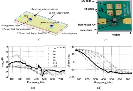
(a) (b)
(c) (d)
Figure 1.25: Performance of non-Foster loaded AMC structure presented by Gregoire et al. in [42]. (a) AMC unit-cell structure, (b) the non-Foster circuit, (c) the reflection magnitude in dB and (d) the reflection phase.
J. Long and D. Sievenpiper proposed using non-Foster circuits to reduce the dispersion of High Impedance Surfaces (HISs) [43]. Different ideal non-Foster L//C were used for obtaining different propagation indexes. Loaded HISs are divergence free in the band (180-450)MHz as shown in Figure 1.26.
(a) (b)
Figure 1.26: Performance of HIS structure presented by Long and D. Sievenpiper in [43]. (a) HIS structure and (b) performance.
Non-Foster circuits can also be used for increasing the operation bandwidth of Split-Ring Resonators (SRRs) [44] and many other applications as in [45, 46, 47, 48].
1.5
NIC Stability
One of the main difficulties of designing non-Foster circuits is their inherent un-stablity due to the positive feedbak. Stephen D. Stearns, studied the stability of


![Figure 1.2: Dipoles bandwidth limits as presented in [20]. (Left) Matching with infinite number of LC and (right) matching with a negative capacitor.](https://thumb-eu.123doks.com/thumbv2/123doknet/8010779.268465/35.893.152.702.184.397/dipoles-bandwidth-presented-matching-infinite-matching-negative-capacitor.webp)
![Figure 1.8: The catalog of NICs circuits given by Sussman-Fort in [25].](https://thumb-eu.123doks.com/thumbv2/123doknet/8010779.268465/38.893.155.783.149.530/figure-catalog-nics-circuits-given-sussman-fort.webp)
![Figure 1.11: The circuit designed by Sussman-Fort Rudisha [28]. (a) Schematic of the circuit and (b) its performance.](https://thumb-eu.123doks.com/thumbv2/123doknet/8010779.268465/40.893.164.785.154.375/figure-circuit-designed-sussman-rudisha-schematic-circuit-performance.webp)
![Figure 1.13: The obtained results by Yifeng et al. in [30]. (a) Input reflection coefficient magnitude and (b) radiation pattern at 200M Hz in E and H plane.](https://thumb-eu.123doks.com/thumbv2/123doknet/8010779.268465/41.893.173.681.140.654/figure-obtained-results-yifeng-reflection-coefficient-magnitude-radiation.webp)