Science Arts & Métiers (SAM)
is an open access repository that collects the work of Arts et Métiers Institute of Technology researchers and makes it freely available over the web where possible.
This is an author-deposited version published in: https://sam.ensam.eu Handle ID: .http://hdl.handle.net/10985/18496
To cite this version :
T. RIBERI – BÉRIDOT, M.G. TSOUTSOUVA, G. REGULA, G. REINHART, Fabrice
GUITTONNEAU, Laurent BARRALLIER, N. MANGELINCK-NOËL - Strain building and correlation with grain nucleation during silicon growth - Acta Materialia - Vol. 177, p.141-150 - 2019
Any correspondence concerning this service should be sent to the repository Administrator : [email protected]
1
STRAIN BUILDING AND CORRELATION WITH GRAIN NUCLEATION DURING SILICON GROWTH
T. Riberi – Béridot1, M.G. Tsoutsouva1,2, G. Regula1, G. Reinhart1, F. Guittonneau3, L. Barrallier3, N. Mangelinck-Noël1
1Aix Marseille Univ, Université de Toulon, CNRS, IM2NP, 13397 Marseille, France
2Presently at Dept. of Physics, Norwegian University Science and Technology, 7491 Trondheim, Norway
3Arts et Métiers Paristech/Institut Carnot Arts Centre Aix-en-Provence 2, cours des Arts et Métiers, 13617 Aix-en-Provence, Cedex 1, France
Abstract:
This work is dedicated to the grain structure formation in silicon ingots with a particular focus on the crystal structure strain building and its implication in new grain nucleation process. The implied mechanisms are investigated by advanced in situ X-ray imaging techniques during silicon directional solidification. It is shown that the grain structure formation is mainly driven by Σ3
<111> twin nucleation. Grain competition phenomena occurring during the growth process lead to the creation of higher order twin boundaries, localised strained areas and associated crystal structure deformation. On the one hand, it is demonstrated that local strain building can be directly related to the characteristics of the twin boundaries created during silicon growth due to grain competition. On the other hand, space restriction due to competition during growth can be at the origin of local strain building as well. Finally, the accumulation of all these factors generating strain is responsible for spontaneous new grain nucleation. When occurring, both grain nucleation and subsequent grain structure reorganisation contribute to lower the strain in the growing ingot. It is demonstrated as well that the local distribution of the strained areas created during silicon growth is retrieved after cooling down, from melting temperature to room temperature, on top of an additional larger scale deformation of the sample due to the cooling down only.
2
1 Introduction
Aiming to the production of low cost and high efficiency silicon based solar cells for photovoltaic (PV) applications, current research focuses on several key targets from silicon purification to cell manufacturing including the silicon ingot fabrication process. When using the conventional multi-crystalline silicon (mc-Si) growth technique, the final silicon grain structure cannot be controlled at all. In addition, the distribution of dislocations is highly inhomogeneous from one grain to another as shown for example by Chen et al.[1]. The presence of dislocations and/or deformed regions can be directly linked to low PV efficiency highlighting their importance for the final properties.Indeed, dislocations play a major role on the efficiency of solar cells, because they can act as preferential segregation sites for impurities, ultimately reducing the carrier lifetime [2-4]. As such, dislocations remain one of the most important efficiency limiting defects in Si for PV applications [5, 6] for which defect engineering is needed [7]. At a higher scale, sub-grain boundaries and sub-grain boundaries of high planar mismatch can be more detrimental than high symmetry grain boundaries such as symmetric coincidence site lattice (CSL) twin boundaries, also due to decoration by impurities [8].
Within this context, three alternative technologies have been proposed to optimize the Si growth process and to improve the crystalline quality of the final ingot. These methods aim at mastering the initial grain nucleation and defect generation from the first stage of solidification: the dendritic casting method [9, 10], the mono-like solidification (ML-Si) [11-13] and the high performance multi-crystalline silicon (HP mc-Si) [14]. Both ML-Si and HP mc-Si techniques, which are used in the industry, produce ingots with a lower dislocation density compared to the conventional mc-Si while allowing the use of low-cost casting solidification methods. However, huge and inherent challenges still exist and are related to: the control of the initial grain nucleation, twinning frequency occurrence, grain competition, defect generation, the interaction of the later with grain boundaries and their evolution during growth so that further research is needed. A major issue shared by all techniques without exception is to control and lower the density of
3
strained regions of the crystal structure that are at the origin of dislocation emission. Few works are available in the literature discussing those phenomena and studying grain formation, grain boundary interaction [15-19] and dislocation generation mechanisms [20-23].
Dislocations can originate from plastic relaxation in deformed crystalline zones. However, it is still not clarified if deformed regions and dislocations develop during both crystal growth and cooling down or only during cooling down. Indeed, the origin of the dislocation or strained regions distribution observed in multi-crystalline silicon is still under debate [23]. The first explanation relies on the formation of dislocations by cooling down due to the Alexander– Haasen model [24]. In this model, during cooling down, inhomogeneity in the stress pattern between different grains due to the solidification step and to the crystallographic orientation creates an inhomogeneous distribution of dislocations linked to the elastic anisotropy of Si single crystal inducing stresses between grains. The second model is based on the local nucleation of dislocation clusters during crystal growth [25] near the solid–liquid interface. These two models to explain dislocation clusters in Si ingots are related to two different steps of the Si ingot fabrication: solidification and cooling down so that it is not possible to propose process improvement methods to reduce dislocation clusters. In the work of Ryningen et al. [23], dislocation clusters were followed as a function of height in a multi-crystalline silicon ingot. From these observations, it was inferred that dislocations should have nucleated during growth oppositely to the cooling down origin mechanism.
Apart from the above controversy, the mechanisms are most likely interlinked as dislocations may originate during growth close to the solid-liquid interface but they can be generated and multiplied due to thermal stress during cooling down as well.
Moreover, recent molecular dynamics simulations of silicon growth highlighted the interrelation between, strain field, dislocation generation relatively to the growth direction and twin nucleation [26].
4
As a consequence, the formation mechanisms of dislocations and of crystal structure deformed regions during solidification must be understood beyond their fundamental interest. There is a need to confirm the strain building dynamics during crystal growth and near the solid-liquid interface at high temperature.
Fundamental understanding of the mechanisms is limited by the difficulty of accessing, from the ex situ study of the solidified ingots, to the origin of deformed and defective areas. The present paper is devoted to the mechanisms involved during the solidification process by advanced in situ characterisation methods. A particular focus is done on the crystal structure strain building during growth and grain competition and to its spreading and its possible role in grain nucleation. This work aims at deepening the fundamental understanding of the strain-related phenomena that occur during the Si crystal growth. Ultimately, this knowledge could be used to optimize the directional solidification processes to reduce the dislocation density and inhomogeneity.
2 Experimental
Solidification furnace and sample
The directional solidification experiment is carried out in a dedicated installation of IM2NP named GaTSBI (Growth at high Temperature observed by Synchrotron Beam Imaging), which is presently installed at beamline ID19 (previously at BM05) at the European Synchrotron Radiation Facility (ESRF). GaTSBI is a unique device that allows following in real time the solidification process during growth. It is a specially designed instrument composed of a high temperature directional solidification (DS) furnace employed in conjunction with synchrotron radiation X-ray imaging techniques (radiography and Bragg diffraction imaging). GaTSBI not only provides information on the solid–liquid interface dynamics, but also gives access to the single grain dynamic evolution during growth, the crystalline orientation / misorientation, the qualitative level of crystal structure local deformation as well as the nature and interaction of structural defects in general. A detailed description of the equipment, of the imaging techniques and of the previously obtained results can be found elsewhere [27, 28].
5
In the present work, the initial monocrystalline Si sample was cut (38 mm × 5.8 mm × 0.3 mm) from a double side mechano – chemically polished intrinsic (resistivity beyond 5000 Ω.cm) FZ wafer 50.8 mm, {110} in surface orientation, provided by SIL’TRONIX Silicon Technologies.
Inside GaTSBI, solidification experiments are performed under dynamic vacuum (~10-6 mbar) while the sample is housed inside a pyrolytic BN crucible with dimensions: length 40 mm, width 6 mm and depth 0.3 mm. The sample is oriented <100>, <110> and < 11�0 > (Figure 1.c) in the solidification direction, in the direction normal to the wafer surface and in the transverse direction, respectively.
Figure 1: White beam diffraction patterns recorded during the experiment: a) initial state after partial melting of the sample to keep an oriented seed: TU (upper resistor) = 1717 K and TL (lower resistor) = 1564 K, b) at the end of the solidification in the field of view: TU (upper resistor) = 1704 K, TL (lower resistor) = 1551 K, c) macroscopic orientation of the initial sample. Applied temperature gradient: 30 K/cm and cooling rate of -1 K/min applied on both heaters. 𝐠𝐠�⃗ is the projection of the diffraction vector on the film.
The sample is heated by applying the same temperature at the bottom and top resistances of the furnace up to 1373 K. Then, a temperature gradient of 30 K/cm is imposed between the two resistive heaters until melting. A local temperature gradient of 12 K/cm was measured in our previous work for this applied temperature gradient [29]. The sample is partially melted and thus a seed crystal, preserving the initial orientation of the sample, is kept within the field of view of the X-ray imaging as can be seen on the diffraction pattern just after partial melting (Figure 1.a). After the partial melting and the stabilization of the solid-liquid interface, a cooling rate of -1 K/min is applied on both heaters until the region of the silicon sample observed within the field
6
of view is fully solidified. Because of the imposed temperature gradient, the solidification is directional in the upward direction. Then, the sample is cooled down until 923 K by applying cooling rates of -13 K/min and -10.4 K/min on the top and bottom heaters, respectively. Below 923 K, the natural cooling down to room temperature of the furnace and sample is not anymore monitored.
In situ X-ray imaging during crystal growth
The sample is constantly illuminated by the X-ray synchrotron white beam during the whole melting, solidification and cooling down sequence. The solid-liquid interface progresses and its morphology is recorded by X-ray radiography using a specific CCD camera developed at the ESRF named FReLoN (Fast Readout Low- Noise) with 2048×2048 image pixel size. An optics giving 5.8 μm pixel size and 11.9 × 11.9 mm2 field of view is used. Radiography images are recorded every 3 s with an exposure time of 1 s. The obtained X-ray radiography images are direct images of the beam transmitted through the sample. The image contrast is based on the material absorption. The absorption coefficient of the solid and liquid Si depends on their mass densities which are not much different (2.31 g/cm3 and 2.56 g/cm3 for solid and the liquid, respectively) meaning that the solid-liquid interface in the raw images is hardly distinguishable. As a consequence, an image processing method consisting of successive image division is applied to reveal the shape of the solid-liquid interface more accurately as explained in our previous work [28].
White beam X-ray Bragg diffraction patterns with a large beam (also named topography) show diffraction spots corresponding to different {hkl} diffracting planes. These diffraction patterns are regularly recorded on X-ray sensitive films (AGFA Structurix D3-SC, 17.6×12.5 cm2) positioned at a distance of about 300 mm from the sample (see for example Figures 1.a and 1.b). In the experiment described in the following, the exposure time used to record the diffraction patterns is 0.5 s. Due to the small beam divergence and to its large size, the whole width of the sample (5.8 mm) can be illuminated; the diffracting volume corresponds to the width of the
7
sample (5.8 mm) × the height of the field of view (10 mm) × the thickness of the sample (0.3 mm). Each diffraction spot contains information on the level of crystal perfection and/or crystal structure strain field. Bragg diffraction imaging consists in studying the detailed structure of diffractions spots. This is a powerful technique that can be used for the visualization of defects (dislocations, twins, domain walls, inclusions, impurity precipitates) present in the crystal volume. Indeed, it allows characterizing the long range distortion fields and / or the strain fields associated with a macroscopic crystal deformation. This is made possible because these distortion fields in the crystal structure diffract at different positions, according to the Bragg law and depending on the different wavelengths of the white beam, compared to the perfect crystal. As a consequence, these distortion fields are at the origin of superimpositions of the diffracted rays, so that a contrast (non – homogeneous intensity distribution) is created in the recorded image and corresponds to crystal structure strain fields [30]. Bragg diffraction imaging technique was used previously by Oriwol et al. [4] to study dislocations and the formation of sub-grain boundaries ex
situ in silicon ingots and by IM2NP in situ during crystal growth (e.g. [18]). The originality of
our work is to combine both radiography and diffraction imaging in situ during growth. Indeed, the combination of both imaging techniques provides complementary dynamic information about crystal growth and competition and about the crystal structure deformation.
Ex situ complementary investigations 2.3.1 Electron Backscatter Diffraction (EBSD)
Ex situ electron backscatter diffraction (EBSD) measurement has been performed after
solidification and cooling down to room temperature using a FEG-SEM JEOL JSM 7001F equipped with a HKL Nordlys camera with either a 7 μm or a 0.7 μm step size depending on the studied area. In order to image the three – dimensional orientation of the crystals in the sample, inverse pole figure (IPF) orientation maps are generated with respect to the three space directions: normal to the sample surface (z), transverse direction (y) and in the growth direction (x). Moreover, the coincidence site lattice map (CSL) is reconstructed to evidence the orientation
8
relationship between adjacent grains and the boundaries with a special character. In this paper, Σ3 <111> (red color in the maps), Σ9 <110> (blue) and Σ27a <110> (yellow) twin boundaries labeling refer to rotations around <h k l> axis that satisfy the misorientation ranges given by the Brandon criterion, which are (60 ± 8.66)°, (38.94 ± 5)° and (31.58 ± 2.89)°, respectively. Additionally, the grain orientation spread (GOS) and local misorientation (LM) maps are extracted as well from the EBSD results. The GOS map is constructed by calculating the difference between the orientation of each pixel in the grain and of the grain average orientation to evidence the more distorted grains within a grain structure. A color code is used to map the grains without deformation (perfect Si crystal appears in blue) and having an average crystal structure deformation (red color for the highest deformation). The LM map provides the local misorientation of each pixel (kernels of 5 × 5 pixels) to locate deformed regions.
3 Experimental results
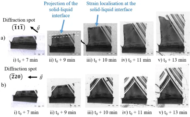
Diffraction spots corresponding to the orientation of the maintained Si seed can be seen in the Figure 1.a. The diffraction pattern recorded after the end of the solidification process at a cooling rate of -1 K/min under an applied temperature gradient of 30 K/cm (TU (upper resistor) = 1704 K and TL (lower resistor) = 1551 K) is displayed in Figure 1.b. Figures 1.a and 1.b confirm that the solidification indeed started from the initial seed oriented <100> along the growth direction (Figure 1.c). New grains nucleated during growth but all keeping an orientation relationship with the initial seed. In the following, the evolution of the (1�11�) and (2�20) spots in particular is investigated during solidification.
Figures 2.a and b show zoomed images of the diffraction spots (1�11�) and (2�20) recorded from the diffraction patterns recorded during solidification. The white dotted lines in Figure 2.a ii) highlight the fact that the projection of the solid-liquid interface can be seen in these images. There is a {111} facet at the solid-liquid interface whose inclination relatively to the sample is directly related to the seed crystal orientation (Figure 1.c) as also seen in our previous work [18].
9
Figure 2: Zoomed images of two diffraction spots extracted from the diffraction patterns during growth (applied temperature gradient: 30 K/cm and cooling rate of -1 K/min applied on both heaters at t0). a) (𝟏𝟏�𝟏𝟏𝟏𝟏�) and b) (𝟐𝟐�𝟐𝟐𝟐𝟐) diffraction spots. t0 corresponds to the beginning of solidification and 𝐠𝐠�⃗ is the projection of the diffraction vector on the film.
After a few millimeters of growth, grains nucleate at the edges of the sample and enter in competition with the initial seed and finally block its progress as can be seen in the sequence of diffraction pattern images recorded during growth in Figure 2. The new grains have a particular orientation relationship with the seed and with each other, they are in twin relationship. This fact is evidenced by the presence of a common diffraction plane, (1�11�), for the left twin crystal and the seed as can be seen by comparing Figures 2.a i) to v) and 2.b i) to v) [28]. Additionally, the zebra aspect and the spots in Figure 2 show that the twins are nucleating regularly during growth and that the crystallographic orientation is alternately repeated. The right zebra pattern is also related to successive twinning. This cannot be evidenced with the diffraction spots showed in Figure 2 but is confirmed by ex situ EBSD characterization (Figure 3).
10
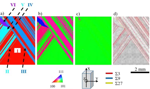
Figure 3: Inverse Pole Figure (IPF) maps obtained by EBSD after growth and cooling down. a) x: along the growth direction, b) z: direction normal to the sample wafer surface, c) y: transverse direction, d) CSL (Coincidence Site Lattice) map.
The final grain structure of the sample after solidification and cooling down is shown by the EBSD Inverse Pole Figure (IPF) maps in Figure 3. The IPF and the CSL maps confirm the successive twinning that occurred during growth (Figure 2) and the competition between the grain growing from the seed (I) and the twin arrays from both right (III) and left (II) sides. Moreover, the repeated succession of identical crystallographic orientations (see the three IPF maps in Figures 3.a to c) is demonstrated. Additionally, the CSL map (Figure 3.d) demonstrates that the newly nucleated grains from the facets at the edges (Figure 4.a) are in twin relationship and in particular at all-time Σ3 twin grains.
Competition among twinned grains takes place as they meet in the middle of the sample. At this level, grain boundaries are formed including Σ3 and in some cases higher order twin CSL boundaries. At last, the right twins take over all other grains as growth proceeds.
11
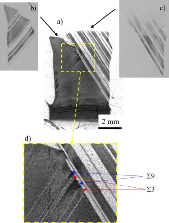
Figure 4: X-ray radiography image of a) the solid-liquid interface during growth with facets at both edges, b) zoom at the level of the grain boundary groove formed due to competition between twins from the left (II) and right (III). The blue lines on Figures 4.a and b correspond to the {111} facet traces. c) Pole figure of the {111} planes issued from the EBSD measurements. The poles of the seed (I), left (II) and right (III) grains are highlighted respectively in red, light blue and dark blue on the pole figure.
As can be noticed in Figure 4, the solid-liquid interface is inclined which indicates the existence of a radial local temperature gradient. The full lines on Figure 4.a corresponds to the inclination of the facets at the edges. These lines are reported on the {111} pole figure (Figure 4.c) and correspond directly to the traces of the {111} planes confirming that the facets observed in Figure 4.a are {111} facets. A first twin nucleation can be observed on the {111} facet situated on the right of the sample and at a later stage on the {111} facet situated on the left. At the level of the edge facets, the measured maximum undercooling is lower than 1 K ranging from 2 × 10⁻¹ to 8 × 10⁻¹ K as previously evaluated [29].
The twins nucleate first at the edges of the sample and grow along the {111} plane towards the center [31]. This sequence is repeated several times during growth on both edges. In this experimental configuration, twins growing from the right and left hand sides reach about the middle of the sample where they meet forming a grain boundary. The corresponding grain
12
boundary groove is evidenced at the solid-liquid interface in Figures 4.a and b. The pole figure of the {111} planes, extracted from the ex situ EBSD measurements, confirms that both grain boundary groove facets are {111} facets (dotted lines on Figure 4) similarly to the edge facets.
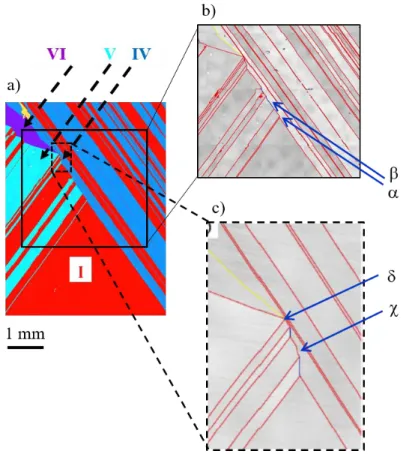
Figure 5: a) Inverse Pole Figure (IPF) map obtained by EBSD after growth along the growth direction (equivalent to Figure 3.a), b) CSL map of the competition region, c) CSL map of the region of the purple grain (VI) nucleation.
When twins from the left side encounter the twins coming from the right side, an alternation of grain boundary types is observed (Figures 5.b and c), successively Σ9 and Σ3. The grain boundary type formed is directly linked to the adjacent grain orientation (Figures 4 and 5).
Concomitantly, strain heterogeneities are observed in the competition region as revealed by the different contrast observed in the Bragg diffraction images (Figures 6.a and d). By the comparison of the CSL maps (Figures 5.b) with the respective diffraction image (Figures 6.d), it can be clearly seen that at the level of Σ3 twin boundaries, no local strain accumulation is observed; whereas the presence of Σ9 twin boundaries induces a localized strain field as evidenced by the black contrast
13
on the diffraction images. Moreover, it is worth noting that the strain created by the grain competition can propagate at longer ranges in the samples as can be seen with the expansion of the black contrast in the right side of the sample (Figure 6.c).
Figure 6: a) �𝟏𝟏𝟏𝟏𝟏𝟏� diffraction spot of the seed and twins at t0 + 13 min during growth (equivalent to Figure 2.a.v), b) complementary spot showing the left twins, c) complementary spot showing the right twins, d) zoom at the level of the growth competition region.
The grain boundary formation at the encounter of twins coming from both sides continues regularly until the dynamics of the competition disturbs the arrangement and a new grain nucleates (grain VI in Figure 7). The nucleation of this grain is of particular interest because it does not take place at the level of the edge facets as for all earlier nucleation during growth. Moreover, it has a different crystallographic orientation from the other previously existing grains. The dynamics of this particular grain nucleation are recorded by X-ray radiography during the solidification (Figure 7). The grain boundary groove created by the encounter of grains IV and
14
V can be seen in the Figures 7.a to d. It is a facetted/facetted grain boundary groove constituted of two {111} facets existing in both grains IV and V as can be seen in the pole figure (Figure 7.f).
Figure 7: Radiography images of the solid-liquid interface at the level of grain IV/V competition leading to the nucleation of grain VI during growth (purple in the IPFX in Figure 3) : a) ti, b) ti + 3 s, c) ti + 6 s, d) ti + 9 s, e) ti + 12 s. f) Pole figure of the {111} planes corresponding to a twin grain on the right (IV, dark blue) and left (V, light blue) sides and to the grain inside the grain boundary groove (VI, purple) from EBSD measurement after crystal growth.
4 Discussion
Nucleation of the twins at the edges of the sample
Σ3 twins nucleate on the {111} facets located at both edges / sides of the sample (left and right). As observed on the radiography images (Figure 4.a), the solid-liquid interface is flat except from the side region where it is inclined. It is higher on the right hand side indicating that there is a transverse temperature gradient which can be estimated from the radiography images to about 0.8 K/cm. The origin of this transverse temperature gradient can be due to the positioning of the sample in the crucible or to its shape after the melting segment creating slight thermal field asymmetries. It is worth noting that it is smaller than the gradient in the vertical solidification direction measured at 12 K/cm which ensures a directional growth in the upward direction as can
15
be seen during the experiment. However, this is sufficient for the right hand side of the interface to be in advance compared to the left hand side. As a consequence, the first twin nucleates on the right hand side {111} facet (Figure 2) and all the subsequent twins nucleating on the right hand side are in advance compared to the twins coming from the left side of the sample. The twin nucleation from the ingot edge has been reported in medium scale [32] as well as in industrial scale mono-like ingots [33]. As a consequence, this phenomenon and the particular final grain structure observed in Figure 3 can be generalised although our samples are small size model ingots.
In our experiments, all twins observed ex situ after growth and after subsequent cooling down to room temperature are issued from the growth segment without exception as can be seen from the comparison between diffraction images during growth (Figure 2) and the grain structure after cooling down (Figure 3). As a consequence, from this experiment as well as from our previous work [18], it is demonstrated that all twins and new grains nucleate during the solidification/growth segment disregarding of shear band phenomena described in the literature [34, 35] as e.g. in wrought magnesium alloys submitted to laser or friction stir welding. In the case of shear band phenomena, a highly twinned microstructure and localized strain is observed. Commin et al. [34]state that during welding, the stored energy is relieved plastically through the shear bands. In our experiments, although twin nucleation is not observed during cooling down, plastic deformation can take place following the Alexander-Haasen [24] model creating dislocations. The initial strain is built at the encounter of grains during growth competition phenomena as will be further discussed in the following.
Twin growth
Once the twin grains have nucleated at the left and right sides of the sample, they grow towards the central part along their respective {111} facets. Since the growth of the right twins is in advance, compared to the left, each time they meet, the growth of the twin grains coming from the left side is blocked. The progress of the pristine grain issued from the seed is also stopped by
16
the left/right twin grain competition (Figures 2 and 3). Due to the higher undercooling at the level of the edge facets compared to the solid-liquid interface, the nucleation on the {111} edge facets is favored and subsequently, edge nucleated twin grains grow at a faster velocity than the general interface [29].
Grain competition and associated strain building
The grain competition between the left and right twins leads to the formation of a groove at the solid-liquid interface and to the generation of a grain boundary.
The grain boundary crystallographic characteristic is directly linked to the relative crystallographic orientations of the two meeting grains. Due to the alternated twin crystallographic orientations, the same grain boundary types are retrieved alternately. In this experiment, Σ3 and Σ9 twin boundaries are formed and are observed in sequence. As mentioned in section 3, strain is not observed at the level of the Σ3 twin grain boundaries whereas local strain is clearly observed each time a Σ9 twin boundary is formed (Figures 5 and 6).
During the heating segment of the experimental procedure, dislocations appear in the sample as seen before [36] and remain in the seed kept after partial melting. During solidification, these dislocations develop, usually along the growth direction and can encounter grain boundaries. Dislocations can be stopped and accumulate, unless they are able to cross-slip at the level of a grain boundary which is most likely to occur at Σ3 type twin boundaries because of the presence of a {111} plane [18]. This situation was also discussed by Lim et al. [37]. They conclude that in nickel, coherent Σ3 twin boundaries act as effective barriers to slip except in the case of screw dislocations which can direct or cross slip across the boundary using the boundary plane itself as a glide plane because it is a {111} plane. Then, the screw dislocations do not leave behind any residual dislocation in the boundary. Ultimately, they can cross slip and propagate along the {111} planes until they reach a free surface or meet another interface. The strained areas observed on the projection of the solid-liquid interface (see Figure 2.a.iii)) and corresponding to the positions
17
of the twin planes can be associated to the gliding of dislocations along the {111} facets that exit at the solid-liquid interface.
Oppositely, local deformed crystal structure zones are created each time a Σ9 twin boundary is formed due to grain competition. This is expected as in the case of Σ9 twin boundaries, cross slip is unlikely. For instance, only the dislocations having the Burgers vector direction of a common rotation axis <110> to build a symmetric grain boundary could cross slip; for other rotation axes, no cross slip is possible. As a consequence, dislocations and strain can accumulate at the level of the Σ9 twin boundary. On top of the local strain, it is observed that the crystal structure strain field can propagate at longer ranges when due to competition by comparison of Figure 6.a and c.
Clearly in our experiments, strain and dislocation emission build during growth as inferred by Ryningen et al. [23]. With these results, it is showed that dislocations and strain can be generated by growth features during solidification only, even though dislocation generation and/or multiplication can occur during heating up and cooling down steps.
Spontaneous grain nucleation inside the grain boundary groove and subsequent strain level decrease
The sequence of the grain boundary groove evolution can be generalized according to our previous work [18, 31] and to the results here. First, when a facetted / facetted grain boundary groove is formed, both facets generally grow at the same growth velocity. If there is no twin relationship between both grains, the direction of the generated grain boundary follows the bisector of the angle between the two facets. This is in agreement with the model proposed by Duffar and Nadri [38, 39]. Ultimately, grain VI nucleation is observed inside the grain boundary groove (Figure 7.e) when it is deeper at this instant as can be seen in Figure 7.d compared to Figure 7.a. A deeper grain boundary groove corresponds to a higher undercooling inside the grain boundary groove which is more favorable for new grain nucleation. Moreover, the new grain nucleation occurs on the left {111} facet of the grain boundary groove that belongs to grain V, as shown in Figure 7.e and as confirmed by the respective {111} pole figures (Figure 7.f).
18
Consequently, a Σ3 twin boundary is formed between grain V and the nucleated grain VI (Figure 5.c).
Several phenomena can concur to the nucleation of the grain VI inside the grain boundary groove. The first reason is that the undercooling inside a grain boundary groove is higher than at the level of the solid-liquid interface as shown in our previous work [29]which facilitates grain nucleation in this area. However, higher undercooling values (ranging 0.2 to 0.8 K) compared to the undercooling inside grain boundary grooves (ranging from 0.1 to 0.4 K) are measured at the edges. It means that the nucleation probability is higher at the edges than inside grain boundary grooves although grain nucleation inside grain boundary grooves remains possible. As a consequence, the main contribution to the grain structure formation is due to nucleation on {111} facets at the edges and the inevitable upcoming grain competition as seen in this experiment.
As seen above, the nucleation of the purple grain VI occurs on the left {111} facet of the grain boundary groove. The attachment energy and the contact area are the key factors for the heterogeneous nucleation of twins as modelled by Jhang et al. [40]. This model was specifically applied to the particular experiment described here and to the grain boundary groove in Figure 7 (Case 1, model 1.1 in [40]). For both facets, the attaching energy of a twin at the level of the crucible wall/Grain IV/Grain V is negative so that twinning is thermodynamically favourable for the experimentally measured undercooling of about 0.4 K [29]. Additionally, from the experimental EBSD data, the 3D configuration of the {111} facets at the level of the grain boundary groove can be quantitatively described. Larger facet angles relatively to the wall are calculated for the left {111} facet in Figure 7 so that it has a lower contact area with the crucible wall. Finally, both low attachment energy and lower contact area concur to a higher twining probability of 8 x 10⁻⁷ on the left facet (facet 1 in reference [40]) compared to the a twinning probability of 8 x 10⁻⁸ on theright facet (facet 2 in reference [40]). Thus, according to this model, the left {111} facet (Grain V in Figure 7) is the most thermodynamically favourable for the
19
nucleation of a new grain. Experimentally, nucleation is indeed observed at the level of this particular {111} facet.
Figure 8: Two possible configurations of the Σ9 twin boundaries between grains of type IV and V in Figure 7, dark and light blue in Figure 5.a, respectively. a) Vertical grain boundary trace (orange lines) corresponding to a Σ9 {122}1,2 twin boundary. Common poles are highlighted by orange circles, b) inclined grain boundary trace (green lines) corresponding to a Σ9 {111}1/{115}2 twin boundary. Common poles are highlighted by green circles.
Additionally, the origin of the nucleation of this grain is due to the competition between twins growing from the left and from the right sides. Indeed, grains are not free to grow due to neighbour grains during competition.
The most stable situation is obtained when the Σ3 twin boundaries formed by competition can follow a common plane {111} or {112}, corresponding to a symmetric coherent and most densely packed and to a symmetric/asymmetric incoherent and second most densely packed Σ3 twin boundary, respectively [41, 42]. In the case of Σ9 twin boundaries, three cases have been reported by Ervik et al. [41]: two twin boundaries with {122} or {114} common planes, the first situation, corresponding to the best crystalline case and to the most densely packed CSL, and an asymmetric Σ9 twin boundary with {111}/{115} planes with a low density of coincidence sites.
20
At the first encounter of twin grains coming from the left and right sides of the sample, a small vertical Σ9 twin boundary is formed (α location in Figure 5.b). This Σ9 twin boundary corresponds to a boundary with a {122} common plane, lying along the macroscopic grain boundary direction as can be seen on the pole figure (orange circles highlight the common poles in Figure 8.a). This is the most stable configuration as the Σ9 {122}1,2 is associated with the lowest energy. Moreover, this boundary is aligned with the temperature gradient which would ensure that both neighbor grains would grow without competition if no further nucleation would occur. However, in the present experiment, subsequent twin nucleation take place on both sample edges as discussed above. Because of competition and of the fact that the twin grains on the right nucleate and grow in advance, the next Σ9 twin boundary cannot develop vertically (β in Figure 5.b). In this case, the Σ9 twin boundary adopts the asymmetric {111}/{115} configuration (common poles are highlighted with the green circles in Figure 8.b)which corresponds to a higher grain boundary energy [43]. This structure has been revealed by TEM (Transmission Electron Microscopy) and its energy has been calculated by DFT (Density Functional Theory) [44]. It was reported that on the contrary to the Σ9 {122}1,2 grain boundary, the atomic structure of the asymmetric Σ9 {111}/{115} one shows strong distortions. Its energy was found to be in the range of the highly symmetric low-Σ GBs but about twice the one of the symmetric Σ9 {122}1,2. As a consequence, this situation is unstable from the energetic point of view and not favorable. During growth, rearrangements tend to create a more stable configuration. Indeed, later during growth, twin grains from the left grow laterally towards the center at the expense of the twin grain from the right. Then, vertical Σ9 {122}1,2 twin boundaries are formed again (Figure 5.c). The important effect of the growth dynamic competition between twin grains coming from the left and right is also evidenced by the presence of a distorted Σ3 twin boundary at first encounter (χ in Figure 5.c) that evolve to the ideal orientation and straightness of the Σ3 twin boundary.
At a later time, at the level of the encounter with a new twin grain from the right (Figures 2.a and b.iv)), a tiny asymmetric Σ9 {111}/{115} twin boundary (δ in Figure 5.c) is created just
21
before the nucleation of the grain VI (purple grain in Figure 5.a). In general, non-symmetrical grain boundaries are deformed at the atomic scale [44] and offer greater resistance for dislocation crossing, thereby creating higher strain [37] and structure deformation, promoting dislocation emission. Concomitantly, an increasing strain is observed. Indeed, the competition goes along with an increasing accumulation of strain when Σ9 twin boundaries are present that can be seen on both diffraction images (Figure 6.d) and grain orientation spread (GOS) in Figure 9.b as well as on the local misorientation (LM) in Figure 9.c EBSD maps.
The local misorientation map (Figure 9.c) gives local information about the strain probably related to the presence of higher density of dislocation clusters. What can be added from the analysis of this map, is that strain accumulates at the twin boundary from the left just before the grain nucleation. Moreover, strain is generated at the encounter of the twins and can propagate in neighbor grains up to several millimeters. As a following step, the grain VI nucleates inside the grain boundary groove on the left {111} facet that belongs to grain V.
The nucleated grain VI is in average less strained than the incoming twins from the right (Figure 9.b). Figure 9.a is a diffraction image of the grain VI on which it can be seen that the highest strain level (darker contrast) is localized at the position of its nucleation and beginning of its growth. Later, the strain level decreases as evidenced by the lighter contrast.
22
Figure 9: a) Diffraction image of the grain VI during solidification at the same instant as Figures 2.a and b.v). b) Grain Orientation Spread (GOS) map, colours range from blue (perfect Si crystal) to red (highest level of the average deformation of the crystal structure) and c) Local Misorientation (LM) map, the highest misorientation corresponding to the red colour. Both GOS and LM maps are extracted from EBSD measurement after growth and cooling down.
On the one hand, after the nucleation, grains above this nucleation event are generally less deformed at the scale of the grain structure (Figure 9.b) and more locally inside the grain that nucleated (Figure 9.a). Indeed, it can be noted that the GOS decreases in average for the last twin (orange color in Figure 9.b) as the nucleation of the grain VI leads to a lower level of distortion in the above growing grains. On the other hand, in the region on the right, after nucleation of the grain inside the grain boundary groove, local strain and dislocation emission (Figure 9.a) are observed. It is due to the competition with the newly nucleated grain that tends to extend in the solidification direction and to the fact that grain VI is incidentally found in a Σ27 twin relationship with the right grain. This type of twin boundary is prone to crystal structure deformation and associated dislocation emission [18, 22].
Strain redistribution cannot be invoked in our experimental case as the existing strain field built during growth remains. However, the new grain nucleation contributes to have a better crystalline
23
quality in the upper part of the ingot. Indeed, after this grain nucleation, the upper growing grains recover a lower strain density.
So, the nucleation can be triggered by energetic reasons discussed above, by grain competition space constraints as well as by the existence of a high density of dislocations that can favor nucleation by decreasing the nucleation undercooling value. It is worth mentioning that this result can be generalized as for the same crystallographic orientation in other samples processed with similar conditions, comparable grain structure can be retrieved and nucleation events similar to the one of the grain VI are observed.
Strain evolution during cooling down
In Figure 10, the evolution of the (2�20) diffraction spot is followed during the cooling down after solidification. A global deformation of the sample is revealed by the evolution of the shape of the diffraction images as clearly seen in Figure 10.e. It corresponds to a bending of the crystal planes at the sample scale. However, although this global strain can be at the origin of dislocations, seeing the very dark contrast of this diffraction image, it is not at the origin of new grains and twin nucleation as can be confirmed by comparing the diffraction images during growth (Figure 2) and the EBSD maps after cooling down (Figure 3). Moreover, another major result is that although there is a clear evolution of the global deformation at the scale of the sample, local strains created during growth still exist after cooling down and are not redistributed as can be seen by comparing the X-ray diffraction images during growth (Figures 6.a & d) and the LM and GOS maps after cooling down (Figures 9.b and c).
As a consequence, one of the main result of this work is also to show that strain that is created during solidification and locally distributed can be retrieved in the ingot after cooling down even though additional sample scale plastic deformation able to generate dislocations is added during cooling down.
24
Figure 10: a) to d) Images of the
(𝟐𝟐�𝟐𝟐𝟐𝟐) diffraction spot during cooling down to 923
K (Applied cooling rate are -13 K/min and -10.4 K/min on the top and bottom
heaters, respectively). e) Image of the
(𝟐𝟐�𝟐𝟐𝟐𝟐) diffraction spot at room temperature.
TU and TL are the temperatures of the upper and lower heaters, respectively. The
same scale is used for all images.
5 Conclusion
Strain building during growth has a high impact on the generation of dislocations but it is also associated to the spontaneous new grain nucleation. It is shown that localized strain building is the result of the twin growth dynamics and competition during growth while the associated dislocation emission mainly depends on the character and the type of the generated twin boundary. One of the main results of this work is that a new grain nucleation can be triggered by the strain accumulation during growth induced by grain competition. Subsequently, this nucleation event contributes to the recovery of a lower strain level in the upper growing grains. The nucleation in presence of strain accumulation can be triggered by energetic reasons as well as by the existence of the associated dislocations. Indeed, dislocations can favor nucleation by decreasing the nucleation undercooling. It is shown that all new grains and twins are only due to nucleation and competition during solidification and are not at all associated to release of plastic deformation during cooling down in the experiment presented here. It should be noted that this also is in agreement with our previous observations.
25
Another main result is that strain, which is created during solidification and non-homogeneously locally distributed, can be retrieved in the ingot after cooling down even though additional strain is created during cooling down. Moreover, no detectable additional twin nucleation is observed during cooling down.
Aknowlegments
The work has been supported by the ANR Project CrySaLID (Nº ANR-14-CE05-0046-01). The ESRF (European Synchrotron Radiation Facility) BM05 team is greatly acknowledged for support during the X-ray imaging experiments.
References