HAL Id: hal-02913151
https://hal.archives-ouvertes.fr/hal-02913151
Submitted on 23 Nov 2020
HAL is a multi-disciplinary open access archive for the deposit and dissemination of sci-entific research documents, whether they are pub-lished or not. The documents may come from teaching and research institutions in France or abroad, or from public or private research centers.
L’archive ouverte pluridisciplinaire HAL, est destinée au dépôt et à la diffusion de documents scientifiques de niveau recherche, publiés ou non, émanant des établissements d’enseignement et de recherche français ou étrangers, des laboratoires publics ou privés.
Chemically vapor deposited Eu 3+ :Y 2 O 3 thin films as
a material platform for quantum technologies
Nao Harada, Alban Ferrier, Diana Serrano, Mauro Persechino, Emrick Briand,
Romain Bachelet, Ian Vickridge, Jean-Jacques Ganem, Philippe Goldner,
Alexandre Tallaire
To cite this version:
Nao Harada, Alban Ferrier, Diana Serrano, Mauro Persechino, Emrick Briand, et al.. Chemically vapor deposited Eu 3+ :Y 2 O 3 thin films as a material platform for quantum technologies. Journal of Applied Physics, American Institute of Physics, 2020, 128 (5), pp.055304. �10.1063/5.0010833�. �hal-02913151�
N. Harada et al., J. Appl. Phys. 128, 055304 (2020)
https://doi.org/10.1063/5.0010833
Chemically Vapour Deposited Eu
3+:Y
2
O
3thin films as a
material platform for quantum technologies
Nao Harada1, Alban Ferrier1, 2*, Diana Serrano1, Mauro Persechino1, Emrick Briand3, Romain
Bachelet4, Ian Vickridge3, Jean Jacques Ganem3, Philippe Goldner1 and Alexandre Tallaire1
1 Chimie ParisTech, PSL University, CNRS, Institut de Recherche de Chimie Paris, 75005 Paris, France 2 Sorbonne Universités, Faculté des Sciences et Ingénierie, UFR 933, 75005 Paris, France
3 INSP, Sorbonne Universités, UPMC Université Paris 6, CNRS, UMR 7588, Paris, France 4 INL, Université de Lyon, Ecole Centrale de Lyon, CNRS UMR 5270, 69134 Ecully, France
Rare earth ions hosted in solids are good candidates for quantum technologies due to their chemical stability and optical and spin transitions exhibiting long coherence lifetimes. While bulk oxide crystals are usually the preferred host material, the development of a scalable silicon-compatible thin film platform would be desirable. In this paper, we report on the growth of Y2(1-x)Eu2xO3 thin films on silicon in the full range of Eu3+ concentration by direct
liquid injection Chemical Vapour Deposition. Our sub-micron polycrystalline films with a strong-(111) texture were grown for all compositions into the bixbyite cubic phase. The variation of growth rates with temperature and flow indicated that deposition occurred through a mass-transport controlled regime. Optical assessment of the Eu-doped thin films showed inhomogeneous linewidths as narrow as 50 GHz and fluorescence lifetimes of 1ms for the lowest concentrations. Finally, a spectral hole was successfully burned in a 200 nm-thin film with a 2 % Eu doping leading to a homogeneous linewidth of 11 MHz. These values are still below those reported for bulk single crystals indicating that additional decoherence mechanisms exist in such nanometric films, which might be alleviated by further improvement of the crystalline quality. Nevertheless, these results pave the way to the use of CVD-grown Eu:Y2O3 thin films as a platform for integrated quantum devices.
1- Introduction
Quantum technologies (QT) are witnessing an increasing interest with the promise to offer new systems and devices with unrivalled performance: ultra-sensitive sensors, quantum computers, information processing, highly-secured communication networks etc1. Often,
these achievements are conditioned by the availability of custom-made materials with exceptional control over the purity as well as defect positioning at the atomic scale. Adopting a stable solid-state, scalable and efficient platform for hosting the required qubits would be advantageous for these devices. Among the various candidates, rare-earth ions (REI) are outstanding as they exhibit extremely narrow optical homogeneous linewidths at low temperature, in the range of a few kHz to less than 100 Hz in bulk single crystals2. This
behaviour stems from their particular electronic configuration in which 4f electrons are shielded from the environment by outer electronic shells3. Optical coherence lifetimes of up
to T2 = 2.6 ms (homogeneous linewidth h = 1/πT2 = 122 Hz) have been reported for
Eu3+:Y
2SiO5 at cryogenic temperatures2 while 151Eu3+ spin transitions that can be optically
addressed, have shown coherence lifetimes up to 10’s of ms4 or even hours5. REI can be
chosen with optical transitions in a wide range of wavelengths, including some that might be relevant for optical fibre telecommunications. In addition, they can be hosted in a variety of matrices and are easily interchangeable due to their chemical similarity. All these properties have for example allowed demonstrating quantum storage6 and quantum state teleportation7
with such systems.
Single crystals produced by crystal pulling techniques such as Czochralski-grown Y2SiO5, are the preferred host for manipulation of large ion ensembles since they provide a
well-controlled environment8,9. These bulk materials are however costly to produce especially
when isotopic enrichment is needed. Due to their size, they also do not provide a platform as appropriated as nano-materials when it comes to integrating REI emitters into other nanoscale systems like high finesse and small volume optical cavities10. Such systems can
enhance RE interactions with light, a pre-requisite to detect the weak emission from single ions11,12. Manipulating single emitters in nanomaterials could indeed potentially unleash
quantum processing and quantum computing applications13. Recently, we have shown that
optical homogeneous linewidths as narrow as 30 kHz14 can be obtained in specially prepared
yttrium oxide (Y2O3) nanocrystals doped with Eu3+ ions, the lowest ever measured for
nanoscale solids15,16. While this value remains above that of bulk crystals, integration of these
nanoparticles into an optical fibre cavity could be successfully obtained10.
Single crystalline thin films constitute an alternative approach. They could possibly allow one to benefit from the flexibility of multi-layers of variable thicknesses with spatially localized emitters and compatibility with scalable platforms like silicon17–20. Integration into a
device or coupling to other quantum materials in a hybrid system21,22 would thus be greatly
facilitated. In the context of QT and high resolution optical spectroscopy, single crystalline films with high purity and low defect content are preferred to achieve an optimized environment for RE ions in which strain, structural defects and electrical or magnetic noise are as limited as possible, possibly leading to extended coherence properties. Indeed, in polycrystalline or even amorphous films, the remaining disorder is expected to induce additional inhomogeneous broadening of the optical linewidths. Epitaxial thin films made by Molecular Beam Epitaxy (MBE) or lifted-off from bulk crystals have been recently investigated and showed promising results18,23,24. Chemical methods have also been explored. Atomic
Layer Deposition (ALD) has been used to deposit thin optically active Eu or Er-doped Y2O3 films
with precise thickness control in the 10-200 nm range and high conformity25. Regarding
optical properties of the emitters, encouraging results have been recently obtained with inhomogeneous linewidth of 200 GHz and 1.5 ms lifetime for the infrared transition of Er-doped ultra-thin films (10 nm)26. However, ALD is limited to a restricted low-temperature
window that does not easily allow for the synthesis of epitaxial oxide films. High temperature post-treatments (950-1050 °C) can partially improve the structural order, but they lead to the formation of parasitic interfacial phases27 as well as unwanted dopant diffusion28 which may
be a limiting factor especially on silicon substrates. Chemical Vapour Deposition (CVD) offers an interesting approach for the deposition of high quality epitaxial RE oxide films due to the possibility to grow under a more flexible range of conditions and higher temperatures29.
Eu3+:Y
2O3 films have already been deposited using standard metal-organic CVD on sapphire,
and inhomogeneous and homogeneous optical linewidths have been reported for films that are several microns thick and high temperature annealed30.
In this work, we used a variant of the CVD technique involving Direct Liquid Injection (DLI) with metal-organic precursors. This technique allow to partially overcomes the issue of low volatility of heavy element precursors as REI ones31–33 and helps having a better control
over their constant feeding inside the reaction chamber. Europium ions doped in Y2O3 were
chosen among other REI in this study because they exhibit ultra-narrow optical homogeneous linewidths and long coherent times while the matrix is a simple cubic binary oxide. Moreover, using this growth technique, almost any other REI or even oxide matrix could be prepared as long as suitable precursors in terms of temperature stability and volatility are outsourced. Deposition was performed on silicon for compatibility with standard wafer processing and silicon-on-insulator waveguide technologies34. A range of deposition conditions were
explored, and highly textured polycrystalline thin films were obtained with a good control over a wide composition range. We provide an assessment of their optical properties and evaluate their relevance to the development of scalable platforms for quantum technologies.
2- Experimental details
To deposit the films, we used a home-made DLI-CVD set-up composed of a double injection and evaporation head (KEMSTREAM Vapbox1500) and a horizontal tube furnace (Carbolite) (Fig. 1). High purity (3N-99.9 %) solid precursors from the -diketonate family (Fig. 1a, Y(TMHD)3 and Eu(TMHD)3) purchased from Strem Chemicals were dissolved in mesitylene
(purity of 99.9%) to obtain concentrations in the range of 0.1-0.01 mmol/L and stored in pressurized tanks. The liquid solution was mixed to a carrier gas (300 sccm of Ar) and brought to the evaporation head maintained at 220 °C where it was sprayed into tiny droplets and flash-evaporated (Fig. 1b). Composition of the films was adjusted by monitoring the opening time and frequency of the two injectors (one for Y and one for Eu). The injectors can be controlled independently allowing a precise control of the incoming molar flow. The gas mixture was then carried through a heated line towards a tubular quartz tube furnace at 750 °C in which Si wafer pieces (10 x 10 mm²) were placed. An additional oxygen flow (150 sccm) was introduced inside the tube. The gases were pumped with a rotary vane pump allowing the pressure to settle at around 10 mbar. Unreacted precursors and chemicals were collected in a nitrogen-cooled trap placed downstream the chamber. Prior to deposition, as-received silicon (100) substrates were cleaned using the standard Radio Corporation of America (RCA) protocol. This includes: first a (1:1:5) solution of (NH4OH:H2O2:H2O) then a 5 %
HF solution and finally a (1:1:5) solution of (HCl:H2O2:H2O). Each step is followed by a deionised
water rinsing. This procedure allows creating a 4 nm-thin, reproducible and stable chemical oxide at the surface of the silicon wafer.
Fig. 1. (a) Schematics of the DLI-CVD set-up used in this study and that uses specially developed liquid injectors.
The reaction chamber consists of a horizontal quartz tube furnace. (b) Chemical representation of Y(TMHD)3
-diketonate precursor used.
Spectroscopic ellipsometry (Woollam iSE) in the range 400-1000 nm was used to evaluate film’s thickness. The ellipsometric angle and phase difference (see supplementary information file, Fig. S1) were recorded at an incidence angle of 65°. The optical refractive index of yttria was obtained using a Cauchy model.
The crystallinity of the films was evaluated using X-ray Diffraction (XRD) in a
PanalyticalXPert Pro diffractometer with a Ge monochromator. Additional high-resolution
(HR) XRD characterisations were performed using a high-brilliance Rigaku SmartLab diffractometer with a 9 kW copper rotating anode and a 2 bounces Ge(220) monochromator.
Chemical composition of the films was obtained by Rutherford Backscattering Spectroscopy (RBS). RBS was performed with a Van de Graaff accelerator, 4He+ particles at
1.8 MeV, 100 nA and a scattering detection angle of 165 °. The areal density of atoms was determined using a reference Si sample implanted with a controlled dose of 209Bi ions (see
supplementary information file, Fig. S3). The spectra were acquired for a 10 µC dose of incident ions for each sample. For Eu concentration below 1 % the doping level could not be precisely assessed by RBS and the nominal doping value was used.
Field Effect Gun Scanning Electron Microscope (FEG-SEM) images of the surface of the films were recorded using a ZEISS Leo 15030 microscope. Micro photoluminescence (µPL) measurements were performed using a Renishaw InVia apparatus with a 50 × objective and a 532 nm laser as the excitation source. Decay measurements at room temperature were also recorded using a tunable optical parametric oscillator pumped by a Nd:YAG Q-switched laser
(Ekspla NT342B-SH) with 6 ns pulse length, an ACTON SP2300i monochromator and a photomultiplier tube. The detection time constant was between 50 µs and 200 µs and data was recorded on a digital oscilloscope (LeCroy 332A).
Inhomogeneous linewidths of the 7F
05D0 transition were measured in reflection
mode using a closed-cycle cryostat (Janis CTI-Cryogenics Model CCS-150) with the temperature monitored by a LakeShore model 330 controller. The 7F
0 5D0 transition
inhomogeneous linewidths were probed by monitoring the fluorescence intensity of the
5D
0 → 7F2 transition at 612 nm as a function of the excitation wavelength around 580.883 nm.
Excitation was provided by a single mode dye laser (Coherent 899-21, 1 MHz linewidth) pumped by a semi-conductor laser (Coherent Verdi G10). Red fluorescence was collected by a 75 mm diameter lens and focused on a photomultiplier tube after suitable filtering to eliminate scattered laser light.
For spectral hole burning (SHB) experiments, samples were cooled down to liquid helium temperatures in a bath cryostat (Janis SVT 200). A continuous wave narrow linewidth (250 kHz) dye laser (Sirah Matisse DS) provided the excitation around 580 nm (7F
0 5D0
transition), which was modulated in time and frequency using an acousto-optic modulator driven by an arbitrary waveform generator (Agilent N8242A). Holes were probed by monitoring the red fluorescence (5D
07F2) at 612 nm, which was collected using a high
numerical aperture lens mounted on a piezo-driven mount and located inside the cryostat. Fluorescence was filtered using low-pass and interferential filters and sent to a high sensitivity photomultiplier tube (Hamamatsu R10699). Further details on the SHB setup used and the procedure are given in the supplementary information file (Fig. S5).
3- Results
3.1- Structural and morphological characterization of the Y2O3 thin films
Undoped Y2O3 thin films were first grown on (100) silicon wafers in order to investigate
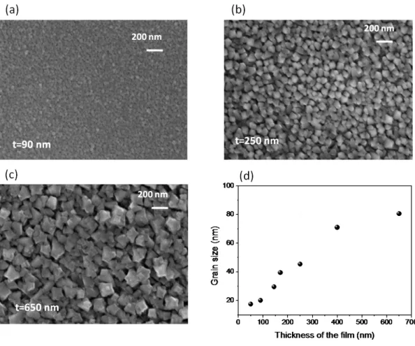
the deposition process by DLI-CVD. By adjusting the deposition time while keeping all other deposition parameters constant, films with thicknesses from 90 to 650 nm as evaluated by ellipsometry (see supplementary information file, Fig. S1) were obtained and observed by SEM. The resulting morphologies are presented in Fig. 2a-c. The films show a polycrystalline structure with an increasing but uniformly distributed grain size from about 20 to 80 nm when increasing thicknesses from 50 to 650 nm and with an obvious saturation of grain coarsening above 400 nm (Fig. 2d). This behaviour is typical from a columnar growth mechanism35 where
nucleated grains competitively grow depending on their faster growth direction until they reach a steady-state.
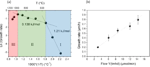
In Fig. 3a, growth rates are plotted as a function of temperature. Below 500 °C no growth is observed due to the well-known limited reactivity of the -diketonate precursors with molecular oxygen36. The use of more powerful oxidizing agents such as ozone would be
a possible way to increase reactivity . At higher temperatures, three regions can be distinguished indicating the different CVD growth modes37. From the slope of the growth rate
dependence with temperature, one can extract the activation energy of the reaction from an Arrhenius law:
ln(𝐺𝑅) = 𝐴 − 𝐸𝑎 𝑅𝑇
where GR is the growth rate, A is a constant, Ea is the activation energy and R is the universal
gas constant. In region I (500-650 °C), growth rates strongly depend on the temperature with an estimated activation energy of 1.2 kJ/mol. This is characteristic of a kinetic regime where
surface reactions are the limiting process. In region II (650-1000 °C), growth rates are less dependent on temperature and activation energy reduces to 0.14 kJ/mol. This indicates that mass transport, i.e. the ability to carry the reactants towards the substrate is the main limiting step. Finally, in region III (T > 1000 °C) the trend is inverted and growth rates continuously decrease with temperature. This can possibly indicate pre-reactions of the precursors that occur before reaching the substrate and that limit the deposition process. This sets the upper temperature bound for this particular CVD system and chemistry.
To confirm that in region II growth rates can be controlled by the supply of the metallic cation precursor, a series of growth runs, in which the Y(TMHD)3 flow was varied from 3 to
14 µmol/min, was carried out at a constant temperature of 750 °C. A linear dependence was found from 0.2 to 0.9 µm/h without any apparent saturation (Fig. 3b). This confirms that mass-transport is the controlling step for growth at this temperature. Although this trend may seem trivial, it indicates that the design of the reactor and the growth conditions (total flow, pressure, concentration etc.) are suitable, avoiding pre-reactions between precursors or uncontrolled turbulent flow inside the chamber.
Fig. 2. (a) –(c) Film morphologies observed by SEM for different thicknesses (t) from 90 to 650 nm showing polycrystalline grains. (d) Grain size directly estimated from SEM images as a function of film thickness.
Fig. 3. (a) Growth rate dependence on temperature showing three distinctive regions. Activation energies are
extracted from the slopes of the lines and are indicated. (b) Y2O3 film growth rate dependence as a function of
the incoming precursor flow at 750°C. This confirms the mass transport regime for region II. The dotted line is a linear fit of the data.
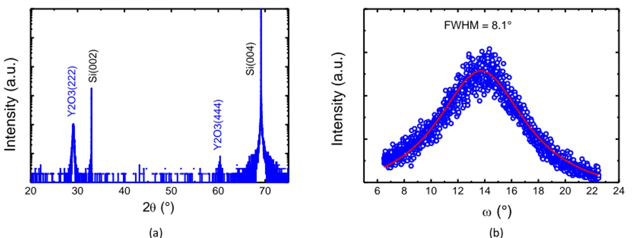
In order to get more insight into the structural properties of the films, HR-XRD analysis was carried out on a 100 nm-thick pure Y2O3 film grown on Si (100). The -2 scan presented
in Fig. 4a shows that the cubic phase of Y2O3was obtained. The position of the peaks is
consistent with a fully-relaxed film. The absence of the (400) diffraction peak and the presence of only (hhh) reflections indicate that the film is (111)-textured. The -scan of Fig. 4b acquired for the (222) lattice plane indicates a relatively high out-of-plane mosaicity of about 8° which shows that an important crystalline disorder exists. Preferential orientation along (111) has already been reported for Y2O3 polycrystalline films obtained by various techniques38,39.Such
texturing is a consequence of the minimization of free surface energy of the grains as well as a competitive growth between grains of different orientations as expected from a columnar growth model. We note that, although all films produced in this study displayed preferential texture, full (111)-texture was only obtained when a thin chemical silicon oxide layer (around 4 nm) was intentionally created by using an RCA cleaning procedure ending with an oxidation step. With as-received silicon substrates, a significant fraction of (100)-oriented grains was found (see supplementary information file, Fig. S2). This suggests that surface preparation of the substrate plays an important role in the texture formation. To assess the in-plane orientation of the films, a pole figure was also acquired on an asymmetric (400) reflection (Fig. 5). The presence of a concentric circle (Fig. 5a) rather than clear diffraction spots in the map underlines that the film was not in-plane oriented. Although no epitaxial growth was obtained here, the full (111)-texture and thus the preferential out-of-plane orientation as well as the relatively narrow diffraction peaks provide positive indicators for the optical properties, even though they do not correspond to specific incorporation sites for the REI. By using appropriate substrates, surface treatments and growth conditions the possibility to epitaxially grow the films on Si will be attempted as already reported for films grown by Molecular Beam Epitaxy (MBE)40,41, Pulsed Laser Deposition (PLD)42 and e-beam evaporation43 for example.
Fig. 4. HR-XRD analysis. (a) -2 scans showing that only the (111)-related diffraction peaks of cubic Y2O3 are observed. (b) scan around the (222) diffraction peak showing an 8° out-of-plane mosaicity. The solid
red line is a Lorentzian fit from which FWHM is extracted.
Fig. 5. (a) Pole figure on the asymmetric (400) reflection from which no preferential in-plane orientation is evidenced. (b) and (c) Line scans at particular values of and.
3.2 Eu doping of the Y2O3 thin films
We then evaluated the ability to produce Y2(1-x)Eu2xO3 films with a controlled doping
and in a wide range of compositions (x = 0 to 1). To this end, a variable amount of Eu(TMHD)3
was added together with Y(TMHD)3 using the double injection head of the DLI-CVD set-up. The
films were grown at 750°C in the mass-transport regime with a 6 µmol/min flow which is a good trade-off between the deposition’s duration and thickness homogeneity on the substrate. To perform RBS measurements, thinner films of 60 nm were grown. Indeed, for too high thicknesses Eu and Y peaks widen and may overlap, further complicating their quantification. The composition of the films was determined using non-channelling conditions
20 30 40 50 60 70 Si(0 04 ) Si(0 02 ) Y2O3( 44 4) Intensity (a.u.) 2 (°) Y2O3( 22 2) 6 8 10 12 14 16 18 20 22 24 (°) Intensity (a.u.) FWHM = 8.1° (a) (b) 0 20 40 60 80 0 15 30 45 60 75 90 105 120 135 150 165 180 0 20 40 60 80 (°) 13.0 38.0 63.0 88.0 113 138 163 188 213 227 Int. (CPS) (°) 0 20 40 60 80 (°) Intensity (a.u.) 0 30 60 90 120 150 180 Intensity (a.u.) (°) (°) 0 90 90 =54° =90° (a) (b) (c)
from the Eu/(Eu+Y) ratio of each related peak in the RBS spectrum (see supplementary information file, Fig. S3). It indicates that incorporation efficiency of Eu and Y in the films was similar. This could be expected since the use of identical ligand molecules in the precursor (TMHD) and the interchangeability of rare-earth elements that possess similar radii and properties are likely to lead to similar chemistry. We note that a systematic cleaning procedure of the injectors between each deposition run using mesitylene solvent was crucial to limit cross-contaminations. This approach allowed us to address a wide Eu range from 0 to 99 % as deduced from RBS analysis. For the highest doping (99 %), background yttrium contamination could not be entirely suppressed despite careful cleaning of the lines preventing reaching a completely pure Eu2O3 film. The crystal structure was then further
analysed by XRD (Fig. 6a). The (222) peak position varied in between the reported values for Y2O3 (a = 10.60 Å) to Eu2O3 (a = 10.87 Å) cubic crystalline structures in a linear fashion (Fig. 6b).
Full solid solution was therefore achieved in agreement with what is expected for cation substitution by the Vegard’s law44. Lanthanide sesquioxides present three major structural
polymorphs: cubic bixbyite, trigonal, and monoclinic. Under ambient conditions, the thermodynamically stable phase of Eu2O3 is monoclinic unlike Y2O3 which is cubic.
Interestingly we note that even for the highest Eu contents, the crystal structure remained in the cubic phase. This might be related to a stabilizing effect of yttrium on the cubic structure or to an influence of the cubic substrate underneath.
Fig. 6. Y2(1-x)Eu2xO3 thin films. (a) Position of the (222) X-ray diffraction peak for different Eu contents measured
by RBS. Vertical dotted lines are the expected values of the two rare-earth oxides in the literature45,46. (b)
Deduced lattice parameter from the peak position using Bragg’s formula. The expected trend for a full solid solution between Y2O3 and Eu2O3 cubic phases are indicated by the red line.
4- Optical properties of the Eu:Y
2O
3thin films
The optical properties of the films grown with different Eu concentrations (thickness around 200 nm) were assessed and benchmarked against Eu:Y2O3 transparent ceramics and
nanoparticles already investigated in our lab. The µPL spectra of films with a similar thickness and Eu content from 1 to 99 % as measured by RBS were recorded using a non-resonant 532 nm excitation laser (Fig. 7a). All spectra were normalized to the samples’ thicknesses. For all compositions, a narrow emission band around 612 nm, corresponding to the 5D
0 7F2 Eu3+
transition in Y2O3 and characteristic of the cubic phase, is observed (Fig. 7b). Furthermore,
integrated intensity of this main emission was found to increase up to concentrations of about 4 % of Eu3+ (Fig. 7c) and then decreases due to concentration quenching, i.e. a reduction of
the emission related to interaction between Eu and defects or impurities (Fig. 7c)47. In
addition, migration of the excitation energy over the Eu3+ sub-lattice increases the probability
of quenching by impurities at higher concentrations. For bulk crystals, the critical concentration was found to be around 10 %48.
The lifetime of the 5D
0 level was then assessed by probing the red fluorescent transition
(5D
0 7F2) following a resonant excitation of the 7F0 5D2 level at 465 nm (Fig. 7a). The
curves in Fig. 6d show a single exponential decay from which the lifetime T1 can be extracted.
T1 exhibits a maximum around 1 ms for the lowest concentrations and then reduces drastically
down to about 36 µs for the highest Eu concentration (Fig. 7e). This is in good agreement with the concentration quenching previously observed in the fluorescence spectra. We note that at a nominal concentration of 1 % the signal was weak and the error in measuring the lifetime was much larger. Nevertheless this maximum lifetime value is comparable to that measured on transparent ceramics with similar Eu3+ doping49 which is an encouraging indicator of
performance of this thin film material.
Fig. 7. Fluorescence and lifetime measurements at room temperature as a function of Eu content estimated by
RBS. (a) Energy level of Eu3+ in Y
2O3 with the 612 nm transition that is monitored. (b) µPL spectra acquired with
a non-resonant 532 nm excitation. (c) Area of the 612 nm PL emission. (d) Fluorescence dynamics of the 5D 0
level obtained by resonantly exciting 5D
2 at 465 nm. (e) Lifetime values determined by fitting the experimental
fluorescence decay curve with a single exponential.
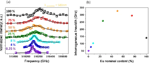
Inhomogeneous linewidths (Γinh) were also evaluated as a function of Eu3+nominal
concentration at a temperature of 10 K. To this end, emission of the 5D
0 7F2 transition was
monitored near 612 nm while the laser excitation frequency was scanned around a central frequency to resonantly probe the 7F
Fig. 8a indicate that, as the Eu content increased, Γinh broadened from a minimum of 50 GHz
(at 0.25 % Eu) to a maximum of 325 GHz (at 50 % Eu). This behaviour is consistent with the fact that the 50 % doping level corresponds to the maximum statistical disorder in the crystal structure where one half of the cations are Y3+ and the other half are Eu3+. A broadening rate
of about 6 GHz per percent of Eu is thus deduced. A blueshift of the line as a function of increasing Eu concentration is also observed, in agreement with the larger Eu ionic radius compared to Y one50,51. The Γ
inh measured here is comparable although slightly narrower than
that reported for ALD-grown and annealed thin films (around 80 GHz at 2 % Eu)26 as well as
CVD-grown and high-temperature annealed films on sapphire (around 90 GHz at 2 % Eu)30.
This relatively low value of inhomogeneous linewidth suggests that RE ions experience a fairly uniform crystalline environment. Nevertheless, at low Eu concentrations, Γinh of our films are
significantly broader than that measured in high-quality nanoparticles annealed at 1200 °C (10 GHz at 0.3 %)15 or transparent ceramics49 of the same composition. This larger
contribution can be attributed to the presence of intrinsic defects such as dislocations or point defects (impurities, vacancies) in the films, indicating that the insertion of Eu3+ ions is not the
main source of broadening at low doping levels. The Lorentzian rather than Gaussian shape of the inh line rather points towards impurities-induced broadening52. We indeed know that
carbon from the precursors or silicon from the substrate might be present in the films. The use of annealing post-treatment at high temperature (> 1100 °C) could possibly help in relieving this issue as demonstrated in Eu:Y2O3 nanoparticles53.
Fig. 8. Inhomogeneous linewidth measurement (a) Emission of the 612 nm line as a function of excitation laser
frequency to probe the 7F
05D0 transition for various Eu concentrations at 10 K. The solid line is a Lorentzian fit
of the experimental data points. (b) Variation of the inhomogeneous linewidth with Eu content.
In order to get more insight into the coherent properties of RE ions in our CVD-grown Eu:Y2O3 thin films, we performed a SHB experiment at 2 K on a 200 nm-thick film with 2 % Eu
doping. Spectral Hole Burning (SHB) is an optical method that can probe homogeneous linewidths and therefore the effect of dynamical fluctuations in the material on RE ion transitions3. In our experiments, the spectral hole is induced by a modification of the
population in the long-lived hyperfine level of the ground state of europium. While at thermal equilibrium all the hyperfine levels are equally populated, a narrow laser excitation can change this population repartition by depleting the pumped hyperfine level (see supplementary information file, Fig. S6). This change of population is directly observed by a
decrease of the red fluorescence emission. Spectral hole width is as broad as twice the homogeneous linewidth provided that it is not increased by other effects like too high excitation power and laser jitter or drift.
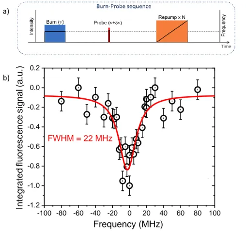
The spectral hole burning sequence used in this work was composed of 3 different parts (Fig. 9a). A burn pulse of 20 ms at a fixed frequency (), a shorter probe pulse at a variable frequency ( + ) and a series of strong pulses scanned over 200 MHz to erase the spectral hole by distributing the population equally between the three hyperfine levels of Eu. The measurement was performed by monitoring the fluorescence intensity after the weak probe pulse. Contribution from laser frequency instability and other hole broadening effects was determined using a Eu:Y2SiO5 single crystal in which the homogeneous linewidth is below
1 kHz. Here a minimal hole linewidth of 2 MHz was recorded, corresponding to the spectral resolution of our setup.
Using the sequence outlined above, we observed a clear spectral hole burning phenomenon with a FWHM of about 22 MHz (Fig. 9b), which gives a homogeneous linewidth of about hom = 11 MHz. This is similar to the value obtained on Eu3+:Y2O3 high temperature
annealed CVD films of higher thickness30 and deposited on sapphire. Nevertheless,
homogeneous linewidths lower by almost two order of magnitude were measured on nanoscale systems (Eu:Y2O3 nanoparticles15,16). The origin of this broadening might be
connected with local disorder that leads to additional dephasing mechanisms known as Two Level System (TLS)30. As discussed above, the large inhomogeneous linewidths observed in the
films is a clear indication of such a disorder. Another homogeneous broadening mechanism suggested in nanoparticles is fluctuating electric fields due, for example, to charge noise on surfaces or grain boundaries15,16. Decreasing these processes could be achieved by reducing
defects and increasing grain or by combining high-temperature deposition and annealing, as well as other post-treatments14. This has proved efficient in obtaining linewidths below
100 kHz in Eu3+:Y
2O3 nanoparticles15,53.Epitaxially depositing the film could also potentially
Fig. 9. (a) SHB sequence used. (b) SHB spectrum obtained when varying the detuning frequency between the
burn and probe pulses. A distinct fluorescence loss is observed indicating an efficient hole burning. The solid line is a Lorentzian fit of the data.
5- Conclusion
Using DLI-CVD we successfully grew Y2(1-x)Eu2xO3 oxide thin films on (100)-oriented
silicon wafers in the full range of Eu content (0 < x < 1). The films obtained through a columnar growth mode were polycrystalline with full (111)-texture. High structural order was achieved for deposition temperatures in the range 650-1050 °C which corresponds to a mass-transport dominated regime. A good control of the solid solution composition was obtained with lattice parameters matching the expected values from a relaxed structure.
The optical properties of such thin films on Si were then assessed and benchmarked against other systems (nanoparticles and ceramics) within the specific context of quantum technologies. Optical spectroscopy showed that fluorescence from the 5D
0 7F2 transition of
Eu3+ ions had strongest emission intensity and longest decay time (1 ms) for low
concentrations (below 4 %). At high concentrations, quenching of the luminescence occurred. The lowest inhomogeneous linewidth was found to be around 50 GHz which is a relatively low value for such a nanoscale system. Notably, a 22 MHz-wide hole was spectrally burned in a 200 nm-thin film on silicon, corresponding to a homogeneous linewidth of 11 MHz. Future efforts to reduce hom should be directed to the improvement of the structural quality of our
Y2O3 thin films and in particular reduce the presence of grain boundaries as well as impurities
and defects that can possibly act as a source of decoherence. Nevertheless, the first structural
-100 -80 -60 -40 -20 0 20 40 60 80 100 -1.2 -1.0 -0.8 -0.6 -0.4 -0.2 0.0 0.2 As deposit Lorentz Fit Fluo re sc en ce Area (U.A.) Frequency (MHz) FWHM = 22 MHz a) b) Int egrat ed fluores c enc e s ignal (a. u .)
and optical assessment indicates that CVD-grown Eu:Y2O3 thin films on silicon offer interesting
perspectives towards their integration into quantum devices.
Supplementary material
See the supplementary material for a more complete description about thickness measurement by Spectroscopic Ellipsometry (SE), effect of silicon surface preparation, composition analysis by RBS, hole burning experimental setup and energy levels of europium.
Acknowledgements
This project has received funding from the European Union’s Horizon 2020 research and innovation programme under grant agreement No 820391 (Square). This research work has received funding from the European Union’s Horizon 2020 research and innovation programme under grant agreement No 712721 (NanOQTech). We acknowledge the financial support of the Paris network on quantum technologies (SIRTEQ), and the French EMIR-A network for provision of irradiation beam time using the SAFIR facility. The authors would also like to thank Hervé Guillon from Kemstream as well as Dominique De Barros for advice and technical support throughout this project.
Data availability
The data that supports the findings of this study are available within the article and its supplementary material.
Bibliography
1 A. Acín, I. Bloch, H. Buhrman, T. Calarco, C. Eichler, J. Eisert, D. Esteve, N. Gisin, S.J. Glaser,
F. Jelezko, S. Kuhr, M. Lewenstein, M.F. Riedel, P.O. Schmidt, R. Thew, A. Wallraff, I. Walmsley, and F.K. Wilhelm, New J. Phys. 20, 080201 (2018).
2 R.W. Equall, Y. Sun, R.L. Cone, and R.M. Macfarlane, Phys. Rev. Lett. 72, 2179 (1994). 3 P. Goldner, A. Ferrier, and O. Guillot-Noel, in Handb. Phys. Chem. Rare-Earth Mater., edited
by Bunzli and Pecharsky (2015), pp. 1–78.
4 A. Arcangeli, M. Lovrić, B. Tumino, A. Ferrier, and P. Goldner, Phys. Rev. B 89, 184305
(2014).
5 M. Zhong, M.P. Hedges, R.L. Ahlefeldt, J.G. Bartholomew, S.E. Beavan, S.M. Wittig, J.J.
Longdell, and M.J. Sellars, Nature 517, 177 (2015).
6 P. Jobez, C. Laplane, N. Timoney, N. Gisin, A. Ferrier, P. Goldner, and M. Afzelius, Phys. Rev.
Lett. 114, 230502 (2015).
7 F. Bussières, C. Clausen, A. Tiranov, B. Korzh, V.B. Verma, S.W. Nam, F. Marsili, A. Ferrier, P.
Goldner, H. Herrmann, C. Silberhorn, W. Sohler, M. Afzelius, and N. Gisin, Nat. Photonics 8, 775 (2014).
8 N. Timoney, B. Lauritzen, I. Usmani, M. Afzelius, and N. Gisin, J. Phys. B At. Mol. Opt. Phys.
45, 124001 (2012).
9 E.Z. Cruzeiro, A. Tiranov, I. Usmani, C. Laplane, J. Lavoie, A. Ferrier, P. Goldner, N. Gisin, and
10 B. Casabone, J. Benedikter, T. Hümmer, F. Oehl, K. de O. Lima, T.W. Hänsch, A. Ferrier, P.
Goldner, H. de Riedmatten, and D. Hunger, New J. Phys. 20, 095006 (2018).
11 R. Kolesov, K. Xia, R. Reuter, R. Stöhr, A. Zappe, J. Meijer, P.R. Hemmer, and J. Wrachtrup,
Nat. Commun. 3, 1 (2012).
12 T. Zhong, J.M. Kindem, J.G. Bartholomew, J. Rochman, I. Craiciu, V. Verma, S.W. Nam, F.
Marsili, M.D. Shaw, A.D. Beyer, and A. Faraon, Phys. Rev. Lett. 121, 183603 (2018).
13 T. Zhong and P. Goldner, Nanophotonics 8, 2003 (2019).
14 S. Liu, D. Serrano, A. Fossati, A. Tallaire, A. Ferrier, and P. Goldner, RSC Adv. 8, 37098
(2018).
15 J.G. Bartholomew, K. de Oliveira Lima, A. Ferrier, and P. Goldner, Nano Lett. 17, 778
(2017).
16 D. Serrano, J. Karlsson, A. Fossati, A. Ferrier, and P. Goldner, Nat. Commun. 9, 2127 (2018). 17 H.J. Osten, A. Laha, M. Czernohorsky, E. Bugiel, R. Dargis, and A. Fissel, Phys. Status Solidi
A 205, 695 (2008).
18 M.K. Singh, A. Prakash, G. Wolfowicz, J. Wen, Y. Huang, T. Rajh, D.D. Awschalom, T. Zhong,
and S. Guha, APL Mater. 8, 031111 (2020).
19 J. Paulraj, R. Wang, M. Sellars, and B. Luther-Davies, Appl. Phys. A 122, 422 (2016).
20 T. Tawara, H. Omi, T. Hozumi, R. Kaji, S. Adachi, H. Gotoh, and T. Sogawa, Appl. Phys. Lett.
102, 241918 (2013).
21 K.J. Tielrooij, L. Orona, A. Ferrier, M. Badioli, G. Navickaite, S. Coop, S. Nanot, B. Kalinic, T.
Cesca, L. Gaudreau, Q. Ma, A. Centeno, A. Pesquera, A. Zurutuza, H. de Riedmatten, P. Goldner, F.J. Garcia de Abajo, P. Jarillo-Herrero, and F.H.L. Koppens, Nat Phys 11, 281 (2015).
22 G. Kurizki, P. Bertet, Y. Kubo, K. Mølmer, D. Petrosyan, P. Rabl, and J. Schmiedmayer, Proc.
Natl. Acad. Sci. 112, 3866 (2015).
23 S. Dutta, E.A. Goldschmidt, S. Barik, U. Saha, and E. Waks, Nano Lett. 20, 741 (2020). 24 S. Wang, L. Yang, R. Cheng, Y. Xu, M. Shen, R.L. Cone, C.W. Thiel, and H.X. Tang,
ArXiv191207584 Phys. (2019).
25 T.T. Van and J.P. Chang, Surf. Sci. 596, 1 (2005).
26 M. Scarafagio, A. Tallaire, K.-J. Tielrooij, D. Cano, A. Grishin, M.-H. Chavanne, F.H.L.
Koppens, A. Ringuedé, M. Cassir, D. Serrano, P. Goldner, and A. Ferrier, J. Phys. Chem. C 123, 13354 (2019).
27 M. Scarafagio, A. Tallaire, M.-H. Chavanne, M. Cassir, A. Ringuedé, D. Serrano, P. Goldner,
and A. Ferrier, Phys. Status Solidi A n/a, 1900909 (2020).
28 B. Lacroix, F. Paumier, and R.J. Gaboriaud, Phys. Rev. B 84, 014104 (2011).
29 R. Lo Nigro, R.G. Toro, G. Malandrino, G.G. Condorelli, V. Raineri, and I.L. Fragalà, Adv.
Funct. Mater. 15, 838 (2005).
30 G.P. Flinn, K.W. Jang, J. Ganem, M.L. Jones, R.S. Meltzer, and R.M. Macfarlane, J. Lumin.
58, 374 (1994).
31 V. Astié, C. Millon, J. M. Decams, and A. Bartasyte, in Chem. Vap. Depos. Nanotechnol.,
edited by Pietro Mandracci (IntechOpen, 2019), pp. 2–23.
32 N. Jehanathan, O. Lebedev, I. Galard, C. Dubourdieu, and G. V. Tendeloo, Nanotechnology
21, 075705 (2010).
33 C. Durand, C. Dubourdieu, C. Vallée, V. Loup, M. Bonvalot, O. Joubert, H. Roussel, and O.
Renault, J. Appl. Phys. 96, 1719 (2004).
34 H. Zhang, J. Yang, J.A. Brown, S. Gray, T.D. Ketcham, B.G. Aitken, and D.A. Nolan, Opt.
35 F. Silva, A. Gicquel, A. Tardieu, P. Cledat, and T. Chauveau, Diam. Relat. Mater. 5, 338
(1996).
36 H.C. Aspinall, in Rare Earth Oxide Thin Films, edited by M. Fanciulli and G. Scarel (Springer
Berlin Heidelberg, Berlin, Heidelberg, 2007), pp. 53–72.
37 H. O. Pierson, in Handb. Chem. Vap. DEPOSITIONCVD, NOYES PUBLICATIONS Park Ridge,
New Jersey, U.S.A. WILLIAM ANDREW PUBLISHING, LLC Norwich, New York, U.S.A. (n.d.).
38 Y.-M. Wu and J.-T. Lo, Jpn. J. Appl. Phys. 4943 (1998).
39 J. Xia, W. Liang, Q. Miao, and D. Depla, Appl. Surf. Sci. 439, 545 (2018).
40 L. Tarnawska, A. Giussani, P. Zaumseil, M.A. Schubert, R. Paszkiewicz, O. Brandt, P. Storck,
and T. Schroeder, J. Appl. Phys. 108, 063502 (2010).
41 R. Bachelet, P. de Coux, B. Warot-Fonrose, V. Skumryev, G. Niu, B. Vilquin, G. Saint-Girons,
and F. Sanchez, CrystEngComm 16, 10741 (2014).
42 M. E. Hunter, M. J. Reed, N. A. El-Masry, J. C. Roberts, and S. M. Bedair, Appl. Phys. Lett.
76, 1935 (2000).
43 C. W. Nieh, Y. J. Lee, W. C. Lee, Z. K. Yang, A. R. Kortan, M. Hong, J. Kwo, and C. -H. Hsu,
Appl. Phys. Lett. 92, 061914 (2008).
44 X. Wu, J.-G. Li, Q. Zhu, J. Li, R. Ma, T. Sasaki, X. Li, X. Sun, and Y. Sakka, Dalton Trans. 41,
1854 (2012).
45 A. Fert, Bull. Société Fr. Minéralogie Cristallogr. 85, 267 (1962). 46 G. Adachi and N. Imanaka, Chem. Rev. 98, 1479 (1998).
47 M. Inokuti and F. Hirayama, J. Chem. Phys. 43, 1978 (1965). 48 M. Buijs, A. Meyerink, and G. Blasse, J. Lumin. 37, 9 (1987).
49 A. Ferrier, C.W. Thiel, B. Tumino, M.O. Ramirez, L.E. Bausá, R.L. Cone, A. Ikesue, and P.
Goldner, Phys. Rev. B 87, 041102 (2015).
50 R.D. Shannon and C.T. Prewitt, Acta Crystallogr. B 25, 925 (1969).
51 S. Welinski, C.W. Thiel, J. Dajczgewand, A. Ferrier, R.L. Cone, R.M. Macfarlane, T.
Chanelière, A. Louchet-Chauvet, and P. Goldner, Opt. Mater. 63, 69 (2017).
52 A.M. Stoneham, Proc Phys Soc 89, 909 (1966).
53 K. de Oliveira Lima, R. Rocha Gonçalves, D. Giaume, A. Ferrier, and P. Goldner, J. Lumin.