HAL Id: tel-02461120
https://pastel.archives-ouvertes.fr/tel-02461120
Submitted on 30 Jan 2020
HAL is a multi-disciplinary open access archive for the deposit and dissemination of sci-entific research documents, whether they are pub-lished or not. The documents may come from teaching and research institutions in France or abroad, or from public or private research centers.
L’archive ouverte pluridisciplinaire HAL, est destinée au dépôt et à la diffusion de documents scientifiques de niveau recherche, publiés ou non, émanant des établissements d’enseignement et de recherche français ou étrangers, des laboratoires publics ou privés.
semi-analytical methods based on the object eigenmodes
Anton Ovcharenko
To cite this version:
Anton Ovcharenko. Modeling of resonant optical nanostructures with semi-analytical methods based on the object eigenmodes. Optics [physics.optics]. Université Paris Saclay (COmUE), 2019. English. �NNT : 2019SACLO019�. �tel-02461120�
nanostructures with semi-analytical
methods based on the object
eigenmodes
Thèse de doctorat de l'Université Paris-Saclay préparée à l’Institut d’Optique Graduate School
École doctorale n°572 Ondes et Matières (EDOM)
Spécialité de doctorat: Physique
Thèse présentée et soutenue à Palaiseau, le 20 Décembre 2019, par
Anton Ovcharenko
Composition du Jury :
Riad Haïdar Président
Directeur de Recherche, ONERA
Xavier Letartre Rapporteur
Directeur de Recherche CNRS, Institut des Nanotechnologies de Lyon
Antoine Moreau Rapporteur
Maître de Conférences, Université Clermont Auvergne
Anne-Laure Fehrembach Examinatrice
Maître de Conférences, Université d'Aix-Marseille
Olivier Gauthier-Lafaye Examinateur
Directeur de Recherche CNRS,
Laboratoire d'Analyse et d'Architecture des Systèmes
Christophe Sauvan Directeur de thèse
Chargé de Recherche CNRS, Institut d’Optique Graduate School
N N T : 20 19 SAC L0 01 9
Cette th`ese est consacr´ee au d´eveloppement de mod`eles semi-analytiques pr´ecis
pour le calcul num´erique de dispositifs nanophotoniques r´esonants. Il s’agit en
parti-culier de membranes `a cristaux photoniques, qui supportent des r´esonances avec des
tr`es grands facteurs de qualit´e, et d’ensembles compos´es de plusieurs nano-antennes
plasmoniques, qui pr´esentent des r´esonances avec des faibles facteurs de qualit´e. La
th`ese est divis´ee en deux parties.
La premi`ere partie pr´esente un mod`ele semi-analytique pour le calcul des modes
support´es par des membranes `a cristaux photoniques. Les modes `a fuite (leaky
modes) support´es par ces membranes structur´ees sont mod´elis´es comme une r´esonance
Fabry-Perot transverse compos´ee de quelques ondes de Bloch propagatives qui vont
et viennent verticalement `a l’int´erieur de la structure. Ce mod`ele est appliqu´e `a
l’´etude des ´etats li´es dans le continuum (bound states in the continuum, ou BIC).
Nous montrons que le mod`ele Fabry-Perot multimode est parfaitement adapt´e pour
pr´edire l’existence des BICs ainsi que leur position dans l’espace des param`etres.
Grˆace `a la semi-analyticit´e du mod`ele, nous ´etudions la dynamique des BICs avec
l’´epaisseur de la membrane pour des structures sym´etriques et asym´etriques. Dans ce
dernier cas, nous ´etudions des objets pr´esentant soit une sym´etrie horizontale bris´ee,
soit une sym´etrie verticale bris´ee (ajout d’un substrat). Le mod`ele Fabry-Perot nous
permet d’obtenir des informations importantes sur la nature et le comportement des
BICs. Nous d´emontrons que lorsque la sym´etrie miroir horizontale est bris´ee, les BICs
dus `a la sym´etrie du syst`eme, qui existent dans les structures sym´etriques au point
Gamma du diagramme de dispersion, restent des BICs malgr´e l’absence de sym´etrie
mais changent de nature. Ils deviennent des BICs dus `a des interf´erences destructives
entre les ondes de Bloch.
La deuxi`eme partie est consacr´ee au d´eveloppement d’une th´eorie modale originale
pour mod´eliser la diffusion de la lumi`ere par des structures complexes compos´ees d’un
ensemble de plusieurs nano-antennes. L’objectif est de pouvoir mod´eliser la diffusion
de la lumi`ere par des m´etasurfaces `a partir de la seule connaissance des modes de
leurs constituants individuels. Pour ce faire, nous combinons un formalisme modal
bas´e sur l’utilisation des modes quasi-normaux (QNM) avec la th´eorie multipolaire de
la diffusion multiple bas´ee sur le calcul de la matrice de transition (matrice T) d’un
diffuseur unique. La matrice T fournit la relation entre le champ incident et le champ
diffus´e dans la base des harmoniques sph´eriques vectorielles. Elle contient toutes les
propri´et´es de diffusion intrins`eques `a l’objet. Le calcul de cette matrice repr´esente une
compr´ehension physique. Nous d´erivons une d´ecomposition modale de la matrice T
et testons sa pr´ecision sur le cas de r´ef´erence d’une nanosph`ere m´etallique.
Enfin, la d´ecomposition modale de la matrice T est appliqu´ee `a des cas pratiques
d’int´erˆet en nanophotonique. A partir de la seule connaissance de quelques modes
d’un nanocylindre plasmonique unique, nous calculons analytiquement la diffusion
multiple de la lumi`ere par un dim`ere et par une antenne Yagi-Uda compos´es de
ces nanocylindres. La comparaison avec les r´esultats d’une m´ethode num´erique
rigoureuse d´emontre un bon accord avec le calcul modal. Par rapport `a des
cal-culs enti`erement rigoureux, la d´ecomposition modale de la matrice T permet une
r´eduction significative du temps de calcul. Comme les calculs sont analytiques une
fois que les modes ont ´et´e calcul´es, l’approche modale est extrˆemement utile pour les
The presented thesis is dedicated to the development of semi-analytical accurate models for the numerical calculation of resonant nanophotonic devices. In particular, it concerns photonic crystal slabs, which can support resonances with high quality factors, and ensembles composed of several plasmonic nanoantennas, which exhibit resonances with low quality factors. The structure of the thesis is two-fold.
In the first part, a semi-analytical model for the calculation of the modes supported by photonic crystal slabs (their dispersion and quality factors) is presented. Leaky modes supported by photonic crystal slabs are modeled as a transverse Fabry-Perot resonance composed of a few propagative Bloch waves bouncing back and forth ver-tically inside the slab. This model is applied to the study of bound states in the continuum (BICs). We show that the multimode Fabry-Perot model is perfectly suit-able to predict the existence of BICs as well as their precise positions in the parameter space. We show that, regardless of the slab thickness, BICs cannot exist below a cut-off frequency, which is related to the existence of the second-order Bloch wave in the photonic crystal. Thanks to the semi-analyticity of the model, we investigate the dynamics of BICs with the slab thickness in symmetric and asymmetric pho-tonic crystal slab. In the latter case, we investigate structures with either a broken horizontal symmetry or a broken vertical symmetry (addition of a substrate). As a result, we obtain some important insights into the nature and behavior of BICs. We evidence that, as the horizontal mirror symmetry is broken, the symmetry-protected BICs that exist in symmetric structures at the Gamma-point of the dispersion dia-gram are still BICs despite the absence of symmetry but change their nature. They become resonance-trapped BICs, but only for specific values of the slab thickness.
The second part of the thesis is dedicated to the development of an original modal theory to model light scattering by complex structures composed of a small ensemble of plasmonic nanoantennas. The objective is to be able to model light scattering by metasurfaces from the sole knowledge of the eigenmodes of their individual con-stituents. For that purpose, we combine a quasi-normal mode (QNM) formalism with the multipole multiple-scattering theory based on the calculation of the so-called transition matrix (T-matrix) of a single scatterer. The T-matrix provides the relation between the incident and scattered fields in the vectorial spherical harmonics basis. It captures all the intrinsic scattering properties of the object that are due to its shape and refractive index distribution. Computation of the T-matrix is a heavy numerical burden since it requires numerous rigorous calculations of the scattered field – one for each harmonic in the basis. Using a modal expansion of the scattered
on the reference case of a metallic nanosphere.
Finally, we apply the modal expansion of the T-matrix to practical cases of interest in nanophotonics. From the sole knowledge of a few modes of a single plasmonic nanorod, we calculate analytically multiple light scattering by a dimer and a Yagi-Uda antenna composed of these nanorods. We apply also the modal approach to a periodic two-dimensional array of nanorods. Comparison with the results of a rigorous Maxwell’s equations solver demonstrates a good agreement with the QNM-based calculation. Compared to fully rigorous calculations, the QNM expansion of the T-matrix allows for a significant reduction of the computation time. Since the calculations are analytical once the modes have been calculated, the QNM approach is extremely useful for optimisation problems.
I Introduction 9
1 Resonant optical nanostructures . . . 10
1.1 Photonic crystal slabs . . . 10
1.2 Metamaterials . . . 12
1.3 Metasurfaces . . . 13
2 Electromagnetic modelling in nanophotonics . . . 16
2.1 Exact analytical solutions . . . 17
2.2 Rigorous numerical methods . . . 18
2.3 Approximate methods . . . 19
3 Outline of the thesis . . . 20
II Bound states in the continuum in photonic crystal slabs 23 1 What is a bound state in the continuum? . . . 24
2 High-contrast photonic crystal slab . . . 25
3 Two types of BICs . . . 27
4 Multimode Fabry-Perot model . . . 30
4.1 Photonic crystal modes as a mixture of Bloch waves . . . . 32
4.2 Transverse resonance for 𝑁 = 1 wave . . . . 35
4.3 Transverse resonance for 𝑁 = 2 waves . . . . 36
4.4 Transverse resonance for 𝑁 = 3 waves . . . . 39
5 Model validation . . . 41
6 Limitations of the model . . . 43
7 Dynamics of BICs with the slab thickness . . . 45
7.1 Symmetric one-dimensional photonic crystal slabs . . . 45
7.2 Asymmetric one-dimensional photonic crystal slabs . . . 49
7.3 Case of a substrate: broken vertical symmetry . . . 51
8 Conclusion . . . 53
III Modal expansion of T-matrix with quasi-normal modes 55 1 Theoretical introduction . . . 57
2.1 Field-based formulation of the T-matrix modal decomposition 73
2.2 Current-based formulation of the T-matrix modal
decompo-sition . . . 74
2.3 Discussion on the difference between the field and the current-based formulations . . . 75
2.4 Cross-sections . . . 76
3 Test case of a sphere . . . 77
3.1 Quasi-normal modes . . . 78
3.2 Reconstruction of the T-matrix . . . 80
4 Conclusion . . . 86
IV Quasi-normal modes based calculation of nonspherical nanoantennas 87 1 Metallic cylindrical nanorod . . . 88
1.1 Quasi-normal modes . . . 89
1.2 Reconstruction of the T-matrix . . . 91
2 Metallic nanorod dimer . . . 93
3 Yagi-Uda nanoantenna . . . 96
3.1 Nanoantenna geometry . . . 97
3.2 Purcell factor of a point source coupled to a dimer antenna 98 3.3 Optimisation of the geometry . . . 100
3.4 Computation of the radiation pattern . . . 102
4 Periodic array . . . 104
5 Computational times . . . 105
6 Conclusion . . . 109
Conclusion 111 A Derivations of the effective reflection coefficients 113 1 Effective coefficients for 𝑁 = 2 waves . . . 113
2 Effective coefficients for 𝑁 = 3 waves . . . 114
B Definition of the vectorial spherical harmonics 117
C Lorentz reciprocity formula 119
D Scattered field formulation 121
Chapter
I
Introduction
Shaping and manipulation of electromagnetic waves is a widespread technique in modern life from radio and microwaves to visible light and X-rays. Glass optical lenses were among the first devices on this path. Now, we use electromagnetic waves in one form or another in virtually every aspect of life, science, and technology, in a way that was not possible before (not to count examples from nature, like eyesight and magnetic-field sensitivity in some birds). As it often happens with a successful piece of technology, we are approaching the limits that conventional optical devices, like common lenses, hit. At the same time, novel technological endeavours and as-pirations demand radically new performance of optical elements. Among them are sub-diffraction limit imaging, smaller footprint, lower energy usage, and higher de-gree of beam manipulation and steering. The field of nanophotonics has emerged as a result with the aim to overcome the Abbe-Rayleigh diffraction limit, developing technology able to manipulate light on a deep-subwavelength scale [1]. As we peer down into the nanoworld, shrinking the photons to atomic sizes, new fundamental physics awaits with the potential of providing monumental technological leaps.
In order to stand up to these challenges we cannot get away with an incremental progress, gradually refining old techniques – totally new approaches are required. Since the advent of micro and nanotechnologies, there have been several new concepts
introduced in the optics and optoelectronics communities. A non-exhaustive list
includes the keywords photonic crystals, plasmonics, nanoantennas, metamaterials, and metasurfaces.
Historically, we can probably begin the countdown with photonic crystals – struc-tures with a periodic variation of optical refractive index, which would act on photons in a similar way a periodic potential acts on electrons in a common solid-state crys-tal [2–8]. Even if surface and volume plasmons were known in solid-state physics [9], plasmonics started to become a research field in its own right with the work on extraordinary optical transmission [10]. The rise of metamaterials started with the experimental demonstration of a negative index of refraction and the theoretical proposal for an appealing application, a perfect lens [11–13]. Nowadays, these are
all well-known building blocks in the nanophotonics toolbox, which are used for an increasingly large number of applications.
In this introduction, we describe a few of these nanophotonic structures and their applications (Section I.1), as well as the numerical methods that can be used to design their optical properties (Sec. I.2). We focus on resonant devices (i.e., devices whose spectral response is characterised by a resonance) for applications in free-space optics. Even if it concerns a large and active community, we do not consider in this thesis nanophotonic structures working in a guided-wave configuration. The last section of this introduction (Sec. I.3) details the outline of the thesis.
1
Resonant optical nanostructures
Resonant nanostructures are key components of modern photonics. They are used for applications as varied as the realisation of nanosources (nanolasers, non-classical light sources), the exploitation of hot spots for the detection of chemical or biological species, the control of light extraction/absorption (LEDs, photovoltaic cells, photode-tectors)... Such a list can only be non-exhaustive as resonant nanostructures occupy a central place in current nanophotonic applications.
If fundamental studies can be realised with single objects, applications often re-quire the use of large-scale arrays, whether periodic, non-periodic, or fully disordered. The large family of resonant nanostructured arrays can be separated into two main categories: the ones with either resonant or non-resonant unit cells. In the latter case, the resonance results from collective effects between several unit cells; typical examples are the phenomena of guided-mode resonance in photonic crystal slabs and light localization in disordered media. In the former case, the resonance of an array can be directly related to the intrinsic resonance of its constituents. Metamaterials and metasurfaces usually belong to this second category.
In the following Sections, we briefly introduce the concepts of photonic crystal slabs, metamaterials, and metasurfaces, as well as their main applications.
1.1 Photonic crystal slabs
Photonic crystals are structures with a periodic variation of refractive index, which would act on photons in a similar way a periodic potential acts on electrons in a common solid-state crystal. First known important endeavours were undertaken by
Lord Rayleigh around 1887 when his nascent experiments with periodic multi-layer dielectric stacks demonstrated a possibility to achieve a photonic band gap in one dimension. A modern phase of these experiments were started almost exactly 100 years later in 1987 by the works of Eli Yablonovitch [3], who coined the term “photonic crystal”, which is so widespread nowadays, and Sajeev John [4].
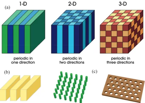
Figure I.1.: Schematic examples of (a) bulk photonic crystals (PhC) with one-, two-, and three-dimensional index modulation; (b) one-dimensional PhC slab; (c) two kinds of 2D PhC slabs – rod slab (square array of dielectric rods in air, left), hole slab (triangular array of air holes in a dielectric slab, right). Images (a) and (c) adapted from [2]
Usually, photonic crystals are made of a high-index dielectric material such as Si or III-V semiconductors with air slits or holes that introduce the periodic order. When their periodicity approaches the wavelength of light, new diffraction effects appear, most notably, a photonic band gap [7], in full analogy with the electronic band gap in a semiconductor. This way, light propagation can be restricted in the direction of periodicity, in one, two, or three dimensions. Then, by introducing defects or wave guiding homogeneous regions, light can be localized or directed in the desired direction [2]. Selecting the geometric parameters of a photonic crystal may not be easy, but if done right we would have a very broad control over light dispersion and therefore also over the propagation speed of a signal.
(1D or 2D) photonic crystal in a dielectric layer of finite (usually subwavelength)
thickness. Compared to three-dimensional (3D) photonic crystals, the simplified
architecture of PhC slabs makes them attractive for on-chip integrated photonics [14, 15]. In addition, their peculiar diffraction properties have been used in a wide variety of applications, including filters [16–20], vertical-cavity surface-emitting lasers (VCSEL) [21–23], photovoltaics [24, 25], thermal emission [26], and structural colour generation [27].
The unit cell of a PhC slab is usually non-resonant on its own. The resonances that can be observed in their reflection and transmission result from the phenomenon of guided-mode resonance, i.e., the coupling of the incident light to a leaky mode supported by the periodic structure [17, 28–33].
1.2 Metamaterials
When the period is much smaller than the operating wavelength, a periodic medium can be accurately described as a homogeneous one with some effective index. This is the basis of so-called Effective Medium Theory (EMT) [34, 35]. By modifying the geometry, the effective index can in principle be engineered to be a specific value thus offering an optical response unavailable using conventional materials. Such structures became known as metamaterials [36–38]. Metamaterials, in broad terms, are artifi-cially designed and fabricated composite materials engineered to have a specific set of predefined desired properties.
Metamaterials with a negative index of refraction are emblematic examples of such artificial structures [11, 12, 39, 40]. However, the concept of structuring a material at a subwavelength scale for modifying its macroscopic properties is more general and has given birth to a much wider range of optical functionalities. A non-exhaustive list includes form birefringence, as originally used by Hertz to polarise radio waves, anti-reflection coatings, diffractive optical elements with enhanced capabilities, and more recently magnetism at optical frequencies and cloaking.
Although this is not always the case, the constituent elements of metamaterials are often resonant on their own. Metamaterials can be ordered, as well as
disor-dered, or possessing some far order [38, 43–46]. In the simplest case of ordered
deep-subwavelength metamaterials, homogenisation techniques can be applied and the metamaterial can be treated as a homogeneous medium with effective permit-tivity and permeability values. In this regime, the design is greatly simplified since one can use well-known analytical results from the theory of homogeneous media. In
Figure I.2.: Typical examples of a split-ring (SSR) resonator for achieving neg-ative effective index of refraction. (a) Schematic of single unit cells orientation with respect to incident wave polarisation and direction. A major parameter is the gap size. (b) SEM image of fabricated sample. Unit cell size is 7× 7μm, nanoring side length is 5 μm. (c) A different example of an asymmetric SSR
with additional degrees of tunability, which are the angles indicated in the fig-ure. (d) An image of a fabricated SSR-based metamaterial for the microwave regime. (a,b) adapted from [41], (c) – [42], (d) – [12].
general, metamaterials in the homogenisation regime are equivalent to anisotropic homogeneous media [47–51]. Mostly because of fabrication constraints, as the work-ing wavelength decreases, the characteristic dimensions of the metamaterial unit cell are not much smaller than the wavelength but only slightly smaller. Thus, opti-cal metamaterials often operate in an intermediate, mesoscopic, regime and their homogenisation becomes questionable [52–54].
1.3 Metasurfaces
Fabricating a bulky piece of 3D metamaterial is a very challenging task, partic-ularly in the frequency range going from the visible to the infrared [38, 43]. As a consequence, last 10 years witnessed a growing interest in 2D planar structures that can be realised with standard nanofabrication processes while preserving an
excep-tional control over the flow of light. The study of planar devices is also driven by the need to mitigate losses and to ease integration into optical elements and circuits. Such metamaterials with a reduced dimensionality are currently called metasurfaces, in the sense that they possess optical properties that go far beyond those offered by conventional flat surfaces [55, 56]. In some sense, by going from 3D to planar struc-tures, the optical metamaterials community has followed a similar path compared to the photonic crystal community with the development of photonic crystal slabs.
Generally, metasurfaces (also known as metalattices or metagratings) come in a form of a two-dimensional array whose unit cells are specifically chosen resonant nanoscatterers, sometimes referred to as meta-atoms. Like metamaterials, subwave-length (especially deep subwavesubwave-length) metasurfaces can be efficiently modelled as homogenised planar sheets (films) with effective parameters [57–62]. The term “met-alens” is often used for metasurfaces that are designed to mimic (and improve upon) the performance of optical lenses [63–68]. They are aimed at achieving wavefront shaping in a general sense (not simply light focusing), mostly in the visible range, while keeping their thickness subwavelength. To achieve a specific wavefront transfor-mation, we need to have a full 2𝜋 phase modulation capability. This requires working close to the resonance of the meta-atoms, often packing multiple elements within one unit cell (itself smaller than the wavelength) each giving a certain phase change in the interval [0, 2𝜋] [69, 70].
In general terms, phase discontinuities on the interface that transform the incident electromagnetic wave into a desired one is the fundamental basis for the functionality of metasurfaces. This idea can be traced back to the Schelkunoff-Huygens princi-ple [71]. Over the years, a substantial work was done to improve the metasurface efficiency [72] and to explore new designs (see, for instance, reviews [55, 73, 74]). Without a doubt, this kind of work will be carried on and expanded further in the following years [75–77].
There are two different types of metasurfaces for the visible and the infrared (see Fig. I.3). The first one employs strongly localised optical resonances induced by metallic nanostructures. This strategy has produced a wide range of devices, such as ultrathin lenses, beam steering devices, and generators of orbital angular momentum of light [78]. The second type of metasurfaces uses arrays of dielectric nanostructures that exhibit geometric Mie-type resonances. This second strategy largely reduces absorption losses [70, 79], enabling high-efficiency beam steering [80], refraction [81], light focusing [82], sensing [83, 84], and holography [85].
Figure I.3.: Scanning electron microscope (SEM) images of two metasurfaces representing important design principles for plasmonic (a) and dielectric (b) devices. The unit cell in (a) is comprised of eight gold nanoantennas optimised to gradually increase the phase delay of the reflected field to cover the whole [0, 2𝜋] interval. The unit cell of the metasurface (b) also has a gradient nature. In this case, however, the size, rather than angle of the nanoantenna is modified in order to achieve a similar effect. Image used in (a) is adapted from [69], (b) – [86].
Metallic nanoparticles, such as silver or gold, are called plasmonic, because their resonant nature results from the free electron collective oscillations (plasmons), which leads to the appearance of localised modes known as localised surface plasmon reso-nances. The resonance (spectral confinement) is associated with a spatial confinement of the electromagnetic field in a small mode volume. However, because of inherent Ohmic losses, especially for infrared and visible regimes, the quality factor of plas-monic resonances remain quite modest, typically in the range 10–50. Ohmic losses mean that some optical energy is being absorbed and transformed into heat. These losses are obviously detrimental for realising efficient optical devices with a high trans-mission or reflection. On the other hand, absorption is the governing effect for other applications, such as biomedical [87] and photo-/thermo-voltaic [88] among others [89].
Increasing the efficiency of metasurfaces by reducing absorption was a major ar-gument for the study of dielectric (with a large refractive index) nanostructures sup-porting Mie-type resonances. Of a particular importance to the field is silicon (other popular choices include germanium, gallium phosphide, titanium dioxide, indium tin oxide or silicon nitride, see, for example, review [84] and references therein). The op-tical properties of such high-index materials are build upon the polarisation charges,
which present inherently lower Ohmic losses. Silicon loss is intrinsically low in the spectral range 0.9—1.65 𝜇𝑚 which has led to the design and implementation of sev-eral Si-based metasurfaces with transmission higher than 90% and full phase agility over the [0, 2𝜋] range [86].
Low losses, while very favourable, is not the only reason for such an enthusiastic development of all-dielectric devices. Planar on-chip fabrication technologies, such as CMOS (Complementary Metal–Oxide–Semiconductor), are well-developed, which would facilitate basic research on metasurfaces, prototyping and eventual potential commercialisation. More crucially, high-index materials possess magnetic-type reso-nances of comparable strength to the electric ones [90, 91]. A strong magnetic dipole resonance occurs due to a coupling of incoming light to a mode characterised by a circular displacement current. This becomes possible when the wavelength 𝜆/𝑛 inside the particle of refractive index 𝑛 becomes comparable to the particle dimension. In contrast, achieving a similar magnetic response with a plasmonic particle requires complex shapes such as split ring resonators [41, 92] or metallo-dielectric composites, such as metal-insulator-metal (MIM) structures [93–95]. In turn, enhanced electro-magnetic fields due to the excitation of the localised surface plasmon resonance in metallic particles can be reproduced with their dielectric counterparts [96]. This is significant as one of the foundational concepts in plasmonics is the large enhancement of the electric field in so-called hot spots. Now, high-index structures are being used to recreate these high electric and magnetic fields concentration spots, while keeping the low losses, to enhance non-linear effects, such as Raman scattering or harmonic generation (see, for example, review [84] and references therein).
The large variety of resonances in dielectric nanostructures enables complex inter-ference phenomena between several excited modes, which in turn drives many novel effects, such as unidirectional scattering [97–101], optical antiferromagnetism [102], optical bound states in the continuum [103, 104], or optical anapoles [103, 105, 106].
2
Electromagnetic modelling in nanophotonics
Since Maxwell’s equations are exact for linear materials, their resolution using rigorous numerical methods has always played a very important role in all fields of electromagnetism. Nanophotonics is a perfect example of this statement. The need for numerical computation is even greater because the cost of manufacturing and characterising a structured object at the nanoscale remains high. Thus, to design a photonic component, it is often better to rely on numerical computations rather than
multiple fabrication-characterisation steps.
However, numerical calculation is not necessarily an easy solution. Indeed, one has to calculate light scattering by 3D structures of complex geometry composed of mate-rials with strong refractive index contrasts (thus, far from the perturbation regime). In the case of metasurfaces, the optical response is a complex interplay between the direct scattering from a single unit cell and the multiple scattering between adjacent unit cells. Moreover, non-periodic metasurfaces are characterised by the coexistence of several length scales with large and small dimensions compared to the wavelength. Finally, given the large number of degrees of freedom, the design and optimisation of devices requires tons of calculations. For these reasons, even though today one has easy access to efficient electromagnetic solvers (both commercial and open-source software products) and powerful computers, and recently optimisation techniques have seen huge progress, modelling the optical response of resonant nanostructures is not an easy task.
As a consequence, a variety of different modelling approaches coexist, from simple toy models to rigorous numerical calculations. In the ensuing sections, we give a brief overview of the main techniques used to model the optical properties of resonant nanostructures.
2.1 Exact analytical solutions
Maxwell’s equations can be solved exactly and analytically for a few specific prob-lems. By analytical, we do not mean here that no computer has to be used, we mean that the electromagnetic field does not need to be discretised, neither spatially nor spectrally. These “analytical” methods rely on the solving of a linear systems of equations. Among these simple geometries, two are of particular interest, even for real devices:
1. Spherical scatterers. Closed form solutions of Maxwell’s equations are provided by Mie theory [107]. Generalisations to spheroids, core-shell spheres, and infi-nite cylindrical rods are available [108–111];
2. Stratified media. Reflection and transmission by a stack of homogeneous layers can be calculated by stacking 2 × 2 matrices that simply contains the Fresnel coefficients, the refractive indices, and the thicknesses of the different layers. These two theories can be extended and combined for the calculation of multiple
scattering by an ensemble of spheres in a homogeneous medium or in a stratified medium [112–115].
2.2 Rigorous numerical methods
Numerical methods that discretise Maxwell’s equations have the advantage to be versatile and can be used, in principle, for any geometry.
The family of finite difference time domain methods (FDTD), along with the related finite difference in the frequency domain methods, is largely used in nanophotonics [116, 117]. Probably, the most widely used version is the one based on the Yee’s algorithm [118]. Yee suggested to have E and H shifted by half of the grid step with respect to each other, and to use central spatial and leapfrog time differences for the derivatives. Finite difference algorithms can be implemented on a 1D, 2D, as well as 3D grid. The meshing typically used is cubic, which suits best for dealing with rect-angular ridges and leads to step-sensitive approximation of curved surfaces (staircase effect). Even though the computations can be parallelised, a typical Cartesian grid causes them to be usually very computationally expensive.
In contrast stand the finite elements methods (FEM) [116, 119]. They do not expe-rience the same hurdles accounting for the geometry as the finite difference methods do thanks to a tetrahedral mesh. Typically, FEM are used in the frequency domain and are built to solve the inhomogeneous vector wave equation, rather than two Maxwell’s equations (Faraday and Ampere’s laws), which is the general approach of the FDTD. The tetrahedral mesh does not just model irregularities in the structure better, it also can accommodate smaller meshing size around features that require finer details, and larger one in the bigger homogeneous regions. This increases the overall computational efficiency greatly compared to FDTD.
Another interesting option is the discrete dipole approximation [116, 120]. The idea is to represent a given nanoparticle with a cubic array of small polarisable blocks with dipolar polarisabilities. Despite not being an exact method and employing a discretisation that may neglect some of nanoparticles fine and curved features, this approach has showed promising performance [121].
These methods rely on a full 3D spatial discretisation of the electromagnetic field and require a large amount of memory in the case of 3D complex objects. On the other hand, modal methods are based on a 2D discretisation and an analytical inte-gration along the third dimension. Such techniques usually handle smaller matrices and result in a smaller computational burden. On the other hand, the matrices are
full in contrast to FDTD and FEM that work with sparse matrices. A widely used modal method is the so-called Rigorous Coupled-Wave Analysis (RCWA) [122–127], also known as the Fourier Modal Method. It is based on an expansion of the electro-magnetic fields onto a basis of Fourier harmonics. RCWA is dedicated to scattering problems with periodic arrays but can also be extended to aperiodic structures [128, 129].
The main advantage of rigorous numerical methods is their versatility. However, they behave as a black box and do not allow for a clear physical understanding of the results. Moreover, as the complexity of the structures to be modelled increases, the number of degrees of freedom explodes, and the optimisation of devices with a rigorous solving of Maxwell’s equations becomes extremely time-consuming.
2.3 Approximate methods
Finally, it is important to mention that numerous approximate methods have been developed for resonant nanophotonics, from toy models to more refined approximate theories. The development of approximate methods is mainly driven by two aspects. First of all, one is rarely fully satisfied with a brute-force calculation and is generally eager to understand the underlying physical mechanism. Secondly, one is always looking for faster calculations in order to accelerate the design and the optimisation of a device.
Widely-used approximate models in nanophotonics are based on the quasi-static approximation. It can be used when the size of the object is much smaller than the wavelength of light. In the context of light scattering by a single object, this approximation stands for the modelling of the scatterer as an electric dipole, whose polarisability is given by a simple analytical expression [116, 130]. In the context of periodic media (photonic crystals, metamaterials), the quasi-static approximation leads to the homogenisation of the structure, so that the new (in general, anisotropic) homogeneous medium can be described by effective optical parameters [34, 130, 131]. In practice, nanophotonic devices do not necessarily fulfil the conditions of the quasi-static approximation. Using such models is then only qualitative. They can help to obtain a coarse physical understanding but they cannot provide accurate predictions. There is clearly some room for improvement, a demand for approxi-mate models that can provide both a good physical understanding and an accurate prediction (i.e., without using fit parameters) of the optical response.
3
Outline of the thesis
The objective of this thesis is to develop semi-analytical models for an efficient mod-elling of periodic and compact resonant optical nanostructures. By semi-analytical, we mean that the models rely on analytical derivations and closed-form expressions that include some physical parameters, which are calculated with a rigorous numerical method. Such an efficient mix between theory and numerical calculation is realised by starting from a rigorous treatment of the electromagnetic problem and substitut-ing some of the steps with well-chosen analytical approximations. In practice, modal methods constitute a perfect choice for applying this recipe. Indeed, taking into ac-count a large number of modes provides a rigorous, virtually exact, result. On the other hand, if the system response is dominated by the excitation of a few modes, neglecting most of the modes still provides accurate, but now semi-analytical, results. This thesis is divided into three chapters.
In Chapter II we present a semi-analytical model for guided-mode resonances in PhC slabs. By making well-chosen approximations in the RCWA, we show that the problem can be treated as a few-modes Fabry-Perot resonator. Further assumptions allow us to derive analytical expressions of the dispersion curve and the quality factor of leaky modes supported by PhC slabs above the light cone. The multimode Fabry-Perot model provides an insightful and efficient procedure to find and study the so-called bound states in the continuum (BICs) – leaky modes of the PhC slab whose coupling to the continuum of the surrounding space vanishes. Thanks to the semi-analyticity of the multimode Fabry-Perot model, we investigate the dynamics of BICs with the slab thickness in symmetric and asymmetric PhC slabs.
Chapter III switches from PhC slabs to finite 3D scatterers, whose resonant na-ture can be accurately described by considering their eigenmodes. This approach, known as quasi-normal mode expansion (or resonant-state expansion), has recently undergone very important developments. Considering a large number of modes pro-vides, in principle, a rigorous solution of the electromagnetic problem. On the other hand, neglecting weakly excited modes to keep only a few dominant ones provides approximate but accurate systems. The semi-analyticity comes in that case from the fact that, once the modes have been calculated rigorously, their excitation coefficient (how strongly a mode is excited by a given incident field) can be derived analyt-ically. We apply quasi-normal mode expansion to the calculation of the scatterer T-matrix, which is an intrinsic characteristic of a scatterer that relates linearly any incident field to the corresponding scattered field. The objective is to subsequently
use the semi-analytical calculation of the T-matrix in a multiple scattering formalism to calculate the response of an ensemble of scatterers from the sole knowledge of a few eigenmodes of its constituents. Despite recent important developments, quasi-normal mode expansion techniques are still less mature than other rigorous numerical meth-ods. Because of this, we test the accuracy of our modal expansion of the T-matrix in cases when either a small or a large number of modes is taken into account. We propose two different modal decompositions and show that one of them provides improved accuracy and convergence speed.
Finally, in Chapter IV, we use the results of the previous chapter and combine the modal expansions of the T-matrices of different objects with a multiple scattering theory. We first calculate analytically the T-matrix of a metallic nanorod from the knowledge of its eigenmodes. Then, we use this modal expansion of the T-matrix to calculate scattering by a dimer of metallic nanorods, emission of a dipole source inserted in a Yagi-Uda antenna composed of metallic nanorods, and absorption in
a periodic array of the same nanorods. In each case, the sole knowledge of the
fundamental mode of the nanorods allows for an approximate reconstruction, which contains most of the physics. Increasing the number of modes improves the accuracy. The results are compared with the rigorous FEM calculation. The strengths and weaknesses of the modal expansion are discussed.
Chapter
II
Bound states in the continuum in
photonic crystal slabs
In this chapter we present a multimode Fabry-Perot model that allows for a simple yet quantitative analysis of the interference mechanism at the origin of the existence of leaky modes in one-dimensional photonic crystal (PhC) slabs. We apply the mul-timode Fabry-Perot model with either two or three Bloch waves (BWs) inside the photonic crystal. For some specific values of the optogeometric parameters, a leaky mode supported by a PhC slab can become a truly guided mode, even if it lies above the light cone, i.e., within the radiation continuum. These are the so-called bound states in the continuum (BICs). Thanks to its semi-analytical character, the model allows for easy calculations of the bound states in the continuum positions in the dispersion diagram and their variation as a function of the slab thickness.
We apply the multimode Fabry-Perot model to the calculation of the dispersion curve and the quality factor of leaky modes supported by 1D PhC slabs of varying thickness. We show that the model is able to quantitatively predict the appearance of bound states in the continuum and their position in the parameter space. We show that, regardless of the slab thickness, BICs cannot exist below a cut-off frequency, which is related to the existence of the second-order Bloch wave in the photonic crystal. Thanks to the semi-analyticity of the model, we investigate the dynamics of BICs with the slab thickness in symmetric and asymmetric photonic crystal slabs.
This chapter is structured as follows. Fist of all, Section II.1 defines and briefly discusses the BIC phenomenon. Following, Sec. II.2 introduces the concept of a PhC slab made of a high refractive index material and comments on its principal opti-cal properties. In Sec. II.3 we introduce and discuss in details to different kinds of BICs that can exist in 1D photonic crystal slabs: symmetry-protected and resonance-trapped. Section II.4 is dedicated to the multimode Fabry-Perot model itself. We begin by presenting the BWs that propagate in a periodic medium and how they can be used to calculate PhC slab dispersion (Subsec. II.4.1). Subsection II.4.2 consid-ers the simplest case of a single propagative BW. Successive Subsections II.4.3 and II.4.4 expand the model for the cases of two and three BWs by reducing them to
the single BW case with effective reflection coefficients. The accuracy of the model is further verified against the Rigorous Coupled Wave Analysis (RCWA) calculation, which takes into account a large set of BWs (Sec. II.5). Its limitations are discussed in Sec. II.6. Finally, leveraging on the semi-analyticity of the model, in Sec. II.7 we study and discuss the behaviour of BICs with varying slab thickness for symmetric (Sub-sec. II.7.1), asymmetric (Sub(Sub-sec. II.7.2), and mounted on a substrate (Sub(Sub-sec. II.7.3) PhC slabs.
1
What is a bound state in the continuum?
In recent years, a lot of interest was generated around the phenomenon of what is now commonly known as bound states in the continuum [103, 104, 132, 133]. A BIC (also called embedded eigenvalue [134]) is a bound state that exists at the same energy level as a continuum of radiation modes [135, 136]. In PhC slabs, it corresponds to an eigenmode that is truly guided (no radiative leakage) despite the fact that it lies above the light cone in the dispersion diagram 𝜔 = 𝑓 (k), with 𝜔 the angular frequency and k the wave vector. In principle, eigenmodes lying above the light cone should be leaky; they are expected to decay as they propagate due to radiative leakage.
The absence of leakage (the fact that the state is bound) originates from two dif-ferent physical mechanisms: symmetry incompatibility between the mode and the radiation continuum for so-called symmetry-protected BICs or destructive interfer-ence between different leakage channels for so-called resonance-trapped or Friedrich-Wintgen BICs [104, 133, 136].
From a strictly theoretical point of view, BICs, and especially the ones resulting from an interference mechanism, are definitely counter-intuitive and intriguing modes. From a practical point of view, however, BICs do not really exist. Indeed, in a real non-ideal structure, they are anyway faintly coupled to the radiation continuum because of technological imperfections, roughness, or finite size of the device. A BIC thereby becomes a leaky mode with extremely low leakage, i.e., with a very large quality factor 𝑄. Therefore, if a PhC slab can be fabricated with geometrical parameters close enough to the ideal ones, it would exhibit a very sharp resonance with an extremely high quality factor whose value is only limited by technological constraints. Such high-𝑄 resonances that result from the existence of a BIC nearby in the parameter space have been recently investigated [137–139] and exploited for lasing [140, 141] and sensing applications [83, 142, 143].
Up to now, the existence of BICs and their location in the parameter space has been calculated either with rigorous numerical methods [104, 140, 144–148] or with various perturbative techniques based on coupled-wave theory [132, 149–152]. Fully numerical approaches are cumbersome even for simple geometries since the whole parameter space has to be explored blindly to find a BIC. In addition, this blind exploration has to be done with a very fine grid since BICs are usually narrow features in the parameter space. Using a perturbation approach is an interesting alternative. However, if coupled-wave theory is accurate for PhC slabs with a low refractive index contrast, the accuracy drops as the contrast increases. Iterative schemes have been proposed to improve the accuracy of the coupled-wave formalism for high refractive index contrasts but at the cost of a drastic loss in simplicity [150].
To ease the practical implementation of PhC slabs supporting BICs, in particu-lar with semiconductor materials, one needs approximate models that yield fast yet accurate predictions of the BIC location in the parameter space. Improving the un-derstanding of the physical mechanisms that lead to the BIC formation is also an important issue. We propose a semi-analytical model that does not rely on a per-turbative approach. The model presents a couple of major advantages. First, it explicitly contains the interference mechanism that leads to the formation of a BIC. And second, it yields quantitative predictions of the corresponding optogeometric parameters for any refractive index contrast.
2
High-contrast photonic crystal slab
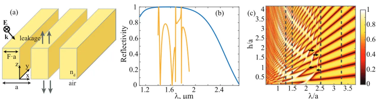
We start with a glance at the optical properties of a lamellar 1D PhC slab, that
is, a periodic array of slits in a dielectric membrane with refractive index 𝑛𝑑 = 3.5
embedded in air, as shown in Fig. II.1(a). The PhC period, the membrane thickness, and the filling factor in dielectric material are respectively denoted with 𝑎, ℎ, and 𝐹 . We study the leaky modes supported by this structure in Transverse Electric (TE) polarisation, i.e., with electric field polarised along the slits in the 𝑦 direction. This structure is also known as a high-contrast grating [153–155].
When a plane wave is incident on the photonic crystal slab, we can distinguish two main operation regimes of a subwavelength photonic crystal slab: resonant and broadband reflector [155]. The two corresponding reflection spectra are depicted in Fig. II.1(b). Since the material is transparent, the transmission is simply given by 𝑇 = 1 − 𝑅. In the resonant regime we can observe sharp Fano features, which is an indication of a plane wave (continuum of the outside free-space modes) coupling to
h a F·a z x y leakage nd air (a) (b) (c) E k 1.2 1.6 2 2.4 l, mm 1 0.8 0.6 0.4 0.2 0 Re fl ec ti vi ty 1 1.5 2 2.5 3 3.5 1 1.5 2 2.5 3 3.5 l/a h/ a 4 0.5 0 1 0.2 0.4 0.6 0.8
Figure II.1.: (a) Schematic of the symmetric 1D PhC slab under study. Main parameters are the PhC period 𝑎, the filling factor F, defined as the fraction
of the dielectric material, the refractive index 𝑛𝑑, and the slab thickness ℎ.
TE-polarised incident field is schematically marked as well. (b) Two regimes of the PhC slab (HCG): broad band reflector (blue line) and resonant (yellow). Parameters are taken from [155]. Namely, for the blue line: 𝑎 = 772 nm,
ℎ = 502 nm, 𝐹 = 0.77, 𝑛𝑑 = 3.2137, TM-polarisation; for the yellow one:
𝑎 = 716 nm, ℎ = 1494 nm, 𝐹 = 0.7, 𝑛𝑑= 3.48, TE-polarisation. (c) Reflectivity
contour of a 1D PhC slab [parameters same as for the reflective regime in (b)] as a function of excitation wavelength 𝜆 and slab thickness ℎ. Black dashed lines mark second to fourth Bloch waves cuttoffs respectively from the right. Arrows point to a region where the Fano resonance feature disappears and BIC emerges.
a discrete leaky state of the PhC slab. This phenomenon is known as a guided-mode resonance. By tuning optogeometric parameters, this feature can be made infinitely narrow until it eventually disappears [see the arrows in Fig. II.1(c)] when leaky mode of the PhC slab becomes a BIC [138]. This means that the discrete leaky state is no longer coupled to the outside space and a BIC emerges.
Figure II.1(c) shows the slab reflectivity colour map versus the normalised 𝜆/𝑎 and the thickness for the case of normal incidence and TE-polarisation. This characteristic pattern exhibits a few distinct regimes of the slab performance, divided by the vertical dashed lines, which correspond to the cut-offs of the BWs that propagate vertically in the periodic medium. The right-most region is the deep-subwavelength (homogenisa-tion) regime, where only a single BW is propagative. One can immediately recognise interference fringes due to the Fabry-Perot mechanism in a homogeneous slab. To the left of it, roughly between 𝜆/𝑎 = 2.5 and 3.3, is the two BWs region. We do not, however, see any interference pattern yet, as, at the normal incidence, the sec-ond BW is decoupled from the outside space and cannot be excited with an incident
plane wave. Shifting farther to the left, we observe an intricate pattern created by the first three BWs interference. Precisely this interference, when totally destructive, leads to the total cancellation of the radiation and emergence of a BIC, and lies in the foundation of the semi-analytical model introduced later in this chapter. As we move further to smaller wavelengths, adding more and more propagating BWs, this pattern becomes more and more complex. The complexity is further exacerbated when diffraction orders emerge, as the wavelength becomes smaller than the period. Let us emphasise that the multimode Fabry-Perot model is particularly well-suited for the study of the resonant behaviour (such as appearance of BICs) of PhC slabs. First, it is derived from a rigorous theory (the RCWA) simply by neglecting evanes-cent waves. Therefore, the BWs used in the model to build the transverse resonance are not virtual intermediary means for the calculation; they have a clear physical meaning, even in the case of structures far from the perturbation regime. They ex-actly correspond to the channels that destructively interfere to form a BIC. Secondly, the BWs are bouncing back and forth vertically inside the PhC slab. The slab thick-ness is thus a crucial parameter to understand the formation of BICs by destructive interference. The model predictions are analytical with respect to this geometrical parameter. Thirdly, BWs possess cut-off frequencies below which they cannot propa-gate. Since the multimode Fabry-Perot model contains them explicitly, the zones in the (𝜔, k) space where BICs of different composition, judging by the number of con-stituent BWs, can exist become apparent with very few calculations. In particular, the model allows us to evidence the existence of a cut-off frequency (related to the second-order BW) below which no BIC can exist, regardless of the slab thickness.
3
Two types of BICs
The eigenmodes of the PhC slab are characterised by a wavevector k = (𝑘𝑥, 𝑘𝑦)
and an eigenfrequency 𝜔˜ = 2𝜋𝑐/𝜆˜. Because of radiative leakage – for modes with a
real wave vector located above the light cone – the eigenfrequencies are complex with a non-zero imaginary part. The latter is related to the mode quality factor,
𝑄 = Re(𝜆˜)/[2Im(𝜆˜)]. (II.1)
Numerical calculations are performed with the RCWA [123]. The leaky modes (or in fact quasi-normal modes, see Chapter III) of the PhC slab are calculated by searching for the poles of the scattering matrix in the complex frequency plane [156, 157]. The
number of Fourier harmonics retained in the expansion of the electromagnetic field is 2𝑀 + 1 with 𝑀 = 30.
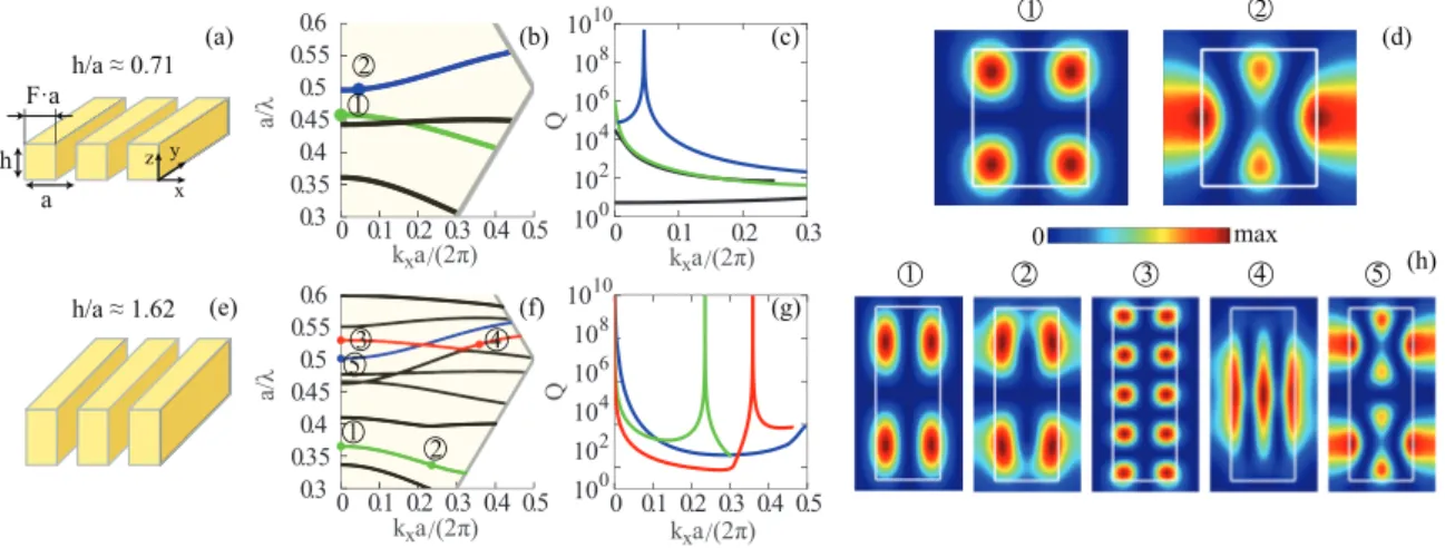
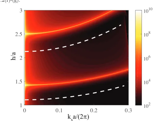
Figure II.2 shows the different types of BICs that can exist in a symmetric 1D PhC slab. It also evidences the crucial role of the slab thickness in the formation of BICs. Figure II.2(b) displays the dispersion curves of the four leaky modes with the
lowest frequency for ℎ = 0.71𝑎 and 𝐹 = 0.6. The normalised frequency 𝑎/Re(𝜆˜) of
the modes has been calculated as a function of the normalised 𝑥-component of the
wavevector 𝑘𝑥𝑎/(2𝜋), which is varied inside the first Brillouin zone, for a fixed 𝑘𝑦 = 0
(non-conical mount). The quality factors of the four modes are shown in Fig. II.2(c). Two modes (green and blue curves) exhibit a BIC along their dispersion curve while the other two (black curves) do not. Indeed, the quality factor of the green mode
diverges for 𝑘𝑥 = 0 and that of the blue mode diverges for 𝑘𝑥 = 0.046(2𝜋/𝑎). The
locations of these two BICs in the dispersion diagram are shown with dots labelled (1) and (2) in Fig. II.2(b). The corresponding electric fields are displayed in Fig. II.2(d).
The existence of the BIC labelled (1) at 𝑘𝑥= 0 (Γ point) can be easily understood:
radiative leakage is prohibited due to symmetry incompatibility. The field profile of
the mode is antisymmetric with respect to 𝑥, 𝐸𝑦(−𝑥, 𝑧) = −𝐸𝑦(𝑥, 𝑧), and it cannot
couple to the symmetric profile of a plane wave with 𝑘𝑥 = 0. 1 These non-leaky
modes had been identified in earlier works on PhC slabs without referring to them as BICs. In recent literature they are often defined as symmetry-protected BICs [104, 133].
The existence of the BIC labelled (2) is more intriguing. Since 𝑘𝑥 = 0, its field
does not present any symmetry. It should, in principle, be coupled to the radiation
continuum. However, radiative leakage is exactly suppressed at 𝑘𝑥 = 0.046(2𝜋/𝑎).
This “accidental” disappearance of leakage results from destructive interference be-tween several leakage channels [104]. In the literature, this type of BIC is referred to as resonance-trapped BIC [133, 140] or Friedrich-Wintgen BIC [136].
As the slab thickness increases to ℎ = 1.62𝑎 (same filling factor 𝐹 = 0.6), more modes appear in the spectral range of interest and the number of BICs increases as well, see Figs. II.2(e)-(h). Our calculations show five BICs whose locations in the dispersion diagram of Fig. II.2(f) are marked with the dots labelled from (1) to (5). The corresponding electric fields are shown in Fig. II.2(h). Figure II.2(g) displays the quality factors of the three leaky modes that exhibit one or two BICs along their
dispersion curve. The green mode has a diverging quality factor at 𝑘𝑥 = 0 and
1Since we plot the absolute value of 𝐸
𝑦 in Fig. II.2, we identify the ones which have zero field
magnitude in the centre of symmetry as antisymmetric. Similarly, a field profile with non-zero magnitude in the central cross-section of the ridge is called symmetric.
0 0.1 0.2 0.3 0.4 0.5 0 0.1 0.2 0.3 0.4 0.5 1 1 2 3 4 5 1 2 3 4 5 0 max 1 2 1 2 h a F·a z x y (a) (b) (c) (d) (e) (f) (g) (h) kx/(2π) 0.3 0.35 0.4 0.45 0.5 0.55 0.6 100 102 104 106 108 1010 Q a/ λ 0 0.1 0.2 0.3 0.4 0.5 0.3 0.35 0.4 0.45 0.5 0.55 0.6 a/ λ 0 0.1 0.2 0.3 100 102 104 106 108 1010 Q a kxa/(2π) kxa/(2π) kxa/(2π) h/a ≈ 1.62 h/a ≈ 0.71
Figure II.2.: BICs in symmetric PhC slabs for two different values of the slab thickness, ℎ = 0.71𝑎 (a)-(d) and ℎ = 1.62𝑎 (e)-(h). (a) and (e) Schematics of the structure. The filling factor and the refractive index of the dielectric
material are fixed, F = 0.6 and 𝑛𝑑 = 3.5. (b) and (f) Dispersion diagrams of
the leaky modes above the light cone (grey line). The bands represented with
coloured curves exhibit BICs for some particular values of the wave vector 𝑘𝑥
shown by coloured dots. (c) and (g) Quality factors 𝑄 of the leaky modes with the same colours as in the dispersion diagram. BICs correspond to Q-factors
that tend to infinity (numerically larger than 109). (d) and (h) Electric-field
distributions |𝐸𝑦(𝑥, 𝑧)| of the BICs shown by coloured dots in (b) and (e). A
single period is represented; edges of the dielectric ridge are shown with white lines.
another one at 𝑘𝑥 = 0.235(2𝜋/𝑎). The first one is a symmetry-protected BIC with
an antisymmetric field profile (1) while the second one is a resonance-trapped BIC with a field profile (2) that is almost antisymmetric but not fully. Similarly, the red
mode is a symmetry-protected BIC at 𝑘𝑥 = 0 [antisymmetric field profile (3)] and
a resonance-trapped BIC at 𝑘𝑥 = 0.3587(2𝜋/𝑎) [field profile (4)]. It is important to
note that the latter has an almost symmetric field profile, see (4) in Fig. II.2(h), in contrast to the resonance-trapped BIC labelled (2), which has a quasi-antisymmetric
field. Finally, the blue mode exhibits a BIC at 𝑘𝑥 = 0. Since its field profile (5) is
symmetric, it cannot be a symmetry-protected BIC but rather a resonance-trapped BIC resulting from destructive interference.
So far, we can only observe in Figs. II.2(f)-(h) that four BICs among five are dif-ferent in nature. Only BICs (1) and (3) are similar; they are symmetry-protected
categories (symmetry-protected and resonance-trapped BICs) is clearly not sufficient to fully characterise BICs in 1D PhC slabs. We summarise in Table II.1 the four dif-ferent types of BICs that can be inferred from Fig. II.2(f)-(h). We will see in Sec. II.4 that the multimode Fabry-Perot model provides a clear physical understanding of the differences between all four types BICs.
First, as already discussed in the literature, BICs can be separated in two families, symmetry-protected BICs and resonance-trapped BICs. For the first ones, leakage is forbidden because of symmetry incompatibility between the mode of the PhC slab and
the radiative plane wave. These BICs can only exist at 𝑘𝑥 = 0; they have necessarily
an antisymmetric field profile. Their existence does not depend on the geometrical parameters of the PhC slab, provided that the horizontal symmetry is conserved. Secondly, leakage can also be suppressed by destructive interference, resulting in the appearance of a resonance-trapped BIC. Figures II.2(f)-(h) evidence that this BIC family can be split in three different subcategories. Resonance-trapped BICs can
exist at 𝑘𝑥 = 0 with a symmetric field profile or at 𝑘𝑥 ̸= 0. In the latter case, the field
profile presents no strict symmetry, but it is either quasi-symmetric [e.g., BIC (4) in Fig. 1(h)] or quasi-antisymmetric [e.g., BIC (2) in Fig. 1(h)]. By the prefix quasi, we mean that the BIC belongs to the dispersion curve of a leaky mode that is either
symmetric or antisymmetric at 𝑘𝑥 = 0. In contrast to the symmetry-protected BICs,
the existence of resonance-trapped BICs formed by destructive interference strongly depends on the geometrical parameters. It is thus difficult to predict their precise position along the dispersion curve.
4
Multimode Fabry-Perot model
Bound states in the continuum in PhC slabs are leaky modes whose radiative leak-age vanishes for a particular set of parameters. Their modelling is intrinsically linked to the phenomenon of guided-mode resonance, which corresponds to the resonant ex-citation of a leaky mode. Over the years, guided-mode resonance has been described by several theoretical formalisms, such as, for instance, coupled-wave theory [30], perturbation methods [32], or polology framework [28, 31]. Of particular interest to the objectives of this thesis is an approach that consists of modelling the reflection and transmission of a PhC slab as a transverse Fabry-Perot resonance composed of a small number of BWs bouncing back and forth inside the slab. This approach has been first proposed as a qualitative interpretation of the high reflectivity of PhC slabs [29]. It has been made quantitative with 𝑁 = 2 waves in 2006 [33]. Then, this
Table II.1.: Classification of BICs in symmetric 1D PhC slabs according to their symmetry properties along the horizontal 𝑥-axis. The symmetry-protected BICs that result from a symmetry incompatibility necessarily have an antisymmetric
field profile at 𝑘𝑥 = 0 and cannot exist at 𝑘𝑥 ̸= 0. The resonance-trapped
BICs formed by destructive interference can exist equally at 𝑘𝑥 = 0 (with a
symmetric field profile) or at 𝑘𝑥 ̸= 0. An antisymmetric (resp. symmetric) field
corresponds to 𝐸𝑦(−𝑥, 𝑧) = −𝐸𝑦(𝑥, 𝑧) [resp. 𝐸𝑦(−𝑥, 𝑧) = 𝐸𝑦(𝑥, 𝑧)]. By
quasi-symmetric (resp. quasi-antiquasi-symmetric), we mean that the field profile of the BIC is almost symmetric (resp. almost antisymmetric), see BICs labelled (2) and (4) in Fig. II.2(h). The last line of the Table gives the number of BWs that interfere to form a BIC. This can be learned from the multimode Fabry-Perot model.
Symmetry-protected Resonance-trapped
BICs BICs
𝑘𝑥 = 0 𝑘𝑥 ̸= 0 𝑘𝑥 = 0 𝑘𝑥 ̸= 0
antisym — sym quasi-sym quasi-antisym
2nd BW — 3rd BW 3rd BW 2nd BW
+1st BW +1st BW +1st BW
+2nd BW
multimode Fabry-Perot model has been used by several authors to study the optical properties of high contrast gratings [153–155].
In what follows, we derive a semi-analytical model that predicts the dispersion curve and the quality factor of leaky modes supported by a PhC slab. We extend the approach proposed in Ref. [33] for the calculation of the reflection and transmission of a PhC slab. In particular, we introduce more analyticity in the calculation. A leaky mode is nothing but a transverse Fabry-Perot resonance composed of several BWs bouncing back and forth vertically inside the slab. This description is perfectly rigorous as long as a sufficiently large number 𝑀 of waves is taken into account.
This is the mathematical ground of RCWA [123]. In the case of subwavelength
periodic structures, only a small number 𝑁 of BWs are propagative, the other ones being evanescent [33, 158]. Neglecting the impact of the evanescent waves provides approximate closed-form expressions that can be very accurate, provided that the slab thickness is large enough, typically larger than the decay length of the least attenuated evanescent wave [33].
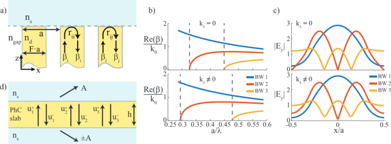
4.1 Photonic crystal modes as a mixture of Bloch waves
Before building a multimode Fabry-Perot resonance in a PhC slab of thickness ℎ, we need to solve the problem of a single interface between a semi-infinite PhC and a
semi-infinite homogeneous medium [see Fig. II.3(a)]. We denote by 𝛽𝑖the propagation
constant of the 𝑖tℎ BW along the vertical 𝑧 direction. In a non-absorbing PhC, 𝛽
𝑖
is either purely real (propagative wave) or purely imaginary (evanescent wave). The
number of propagative BWs depends on the geometry. For example, for 𝑘𝑥 = 0,
𝐹 = 0.6, and 𝑛 = 3.5, only up to three BWs are propagative in the band 𝑎/𝜆 < 0.6. Their propagation constants are shown in Fig. II.3(b), where we can observe the second and third BW cut-offs at 𝑎/𝜆 = 0.327 and 𝑎/𝜆 = 0.45, respectively. Note that the fundamental BW (largest propagation constant, blue curve) has no cut-off
and is propagative regardless of the 𝑎/𝜆 value. The corresponding field profiles 𝐸𝑦(𝑥)
are shown in Fig. II.3(c). The fundamental BW is symmetric and the higher-order
BWs have alternately an antisymmetric or a symmetric field profile. For 𝑘𝑥 ̸= 0, the
cut-off frequencies vary with 𝑘𝑥 and the BWs are no longer strictly symmetric nor
antisymmetric.
As the 𝑖tℎ BW is incident on an interface with a homogeneous medium, it is
re-flected with a reflection coefficient 𝑟𝑖𝑖. In addition, it is reflected into a different BW
with a cross-reflection coefficient 𝑟𝑖𝑗, and transmitted as a propagative plane wave
with a transmission coefficient 𝑡𝑖. The coefficients 𝑟𝑖𝑖, 𝑟𝑖𝑗, and 𝑡𝑖 are the generalised
Fresnel coefficients for an interface between homogeneous and periodic media. Note that we limit ourselves to the case where a single plane wave is propagative in the homogeneous medium – the zeroth diffraction order of the PhC slab. The energy contained in this plane wave corresponds to the radiative leakage.
In a PhC slab of thickness ℎ, the BWs are reflected at the top and bottom interfaces. Thus, they propagate back and forth inside the slab, as illustrated in Fig. II.3(d).
We denote by 𝑢+𝑖 and 𝑢−𝑖 the amplitudes of the up- and down-propagating 𝑖tℎ wave,
respectively. The phase origin for the amplitude 𝑢+𝑖 (resp. 𝑢−𝑖 ) is taken at the bottom
interface (resp. the top interface).
Leaky modes of a PhC slab are solutions of Maxwell’s equations in the absence of an incident wave. If one considers a finite number 𝑀 of BWs (propagative and
z x rii nd ngap ns a) bi bi rij bi bj ns ns d) PhC slab u1+ -u2 u3 u1 u2 u3 + + -- h A ±A BW 1 BW 2 BW 3 0 1 2 0.250.3 0.350.4 0.45 0.5 0.55 0.6 a/l Re(b) k0 Re(b) k0 b) 0 1 2 0 1 2 3 |Ey| x/a -0.50 0 0.5 1 2 3 BW 1 BW 2 BW 3 c) |Ey| kx ≠ 0 kx = 0 kx ≠ 0 kx = 0 F·a a
Figure II.3.: Multimode Fabry-Perot model. (a) Interface between a
semi-infinite PhC and a homogeneous medium. The refractive index of the
homoge-neous medium 𝑛𝑠can be different from the index 𝑛gapinside the slits of the PhC.
At the interface, the Bloch waves (propagation constants 𝛽𝑖) propagating in the
periodic medium are reflected with a reflection coefficient 𝑟𝑖𝑖, cross-reflected
with a reflection coefficient 𝑟𝑖𝑗, or transmitted with a transmission coefficient
𝑡𝑖. (b) Normalised propagation constants of the BWs for 𝐹 = 0.6 as a function
of the frequency at the Γ-point (𝑘𝑥 = 0) and at 𝑘𝑥 = 0.2𝑎/(2𝜋). The cut-off
frequencies of the second and third BWs are shown by vertical dashed lines.
(c) Electric-field profile |𝐸𝑦(𝑥)| of the three propagative BWs for 𝑎/𝜆 = 0.526.
(d) Principle of the multimode Fabry-Perot model. In the spectral range of interest, up to three BWs can propagate back and forth inside the PhC slab, all other BWs being evanescent. Each BW is transmitted in the surrounding medium with its own phase. The amplitude 𝐴 of the plane wave propagat-ing away (radiative leakage) results from the interference between these three contributions. 𝑢+𝑖 = 𝑀 ∑︁ 𝑗=1 𝑟𝑗𝑖𝑢−𝑗 exp(𝑖𝛽𝑗ℎ), 𝑢−𝑖 = 𝑀 ∑︁ 𝑗=1 𝑟𝑗𝑖𝑢+𝑗 exp(𝑖𝛽𝑗ℎ). (II.2)
The number 𝑀 of BWs is equal to the truncation rank of the Fourier series in RCWA [123], 𝑀 = 30 for the calculations shown in Fig. II.2. For the sake of simplic-ity, we consider a PhC slab surrounded by the same homogeneous medium above and