Carrier transport properties in the vicinity of single self-assembled quantum dots
determined by low-voltage cathodoluminescence imaging
E. Dupuy, D. Morris, N. Pauc, V. Aimez, M. Gendry, and D. Drouin
Citation: Appl. Phys. Lett. 94, 022113 (2009); doi: 10.1063/1.3072613 View online: http://dx.doi.org/10.1063/1.3072613
View Table of Contents: http://aip.scitation.org/toc/apl/94/2 Published by the American Institute of Physics
Carrier transport properties in the vicinity of single self-assembled
quantum dots determined by low-voltage cathodoluminescence imaging
E. Dupuy,1,3D. Morris,1N. Pauc,2,a兲V. Aimez,2M. Gendry,3and D. Drouin2,b兲
1CNR2, Département de Physique, Université de Sherbrooke, Sherbrooke, Quebec J1K2R1, Canada 2CNR2, Département de Génie Électrique et Génie Informatique, Université de Sherbrooke, Sherbrooke,
Québec J1K2R1, Canada
3Institut des Nanotechnologies de Lyon, Ecole Centrale de Lyon, INL-UMR5270/CNRS, 69134 Ecully,
France
共Received 19 November 2008; accepted 23 December 2008; published online 16 January 2009兲 We propose a method to investigate the carrier transport properties in the ultrathin wetting layer of a self-assembled quantum dot 共QD兲 structure using low-voltage cathodoluminescence 共CL兲 imaging. Measurements are performed on diluted InAs/InP QDs in order to spatially resolve them on CL images at temperature ranging from 5 to 300 K. The mean ambipolar diffusion length extracted from CL intensity profiles across different isolated bright spots is about 300 nm at 300 K. This gives an ambipolar carrier mobility of about 110 cm2/共V s兲. Temperature investigation reveals
a maximum diffusion length near 120 K. © 2009 American Institute of Physics. 关DOI:10.1063/1.3072613兴
With the development of solid-state optoelectronic de-vices based on single self-assembled quantum dots 共QDs兲 such as nanolasers or single photon sources, evaluation of their individual properties is fundamental. As well as the study of single dot emission, investigation of carrier trans-port from their generation point in the barrier to their capture and relaxation into QDs is relevant for the improvement of device performances.1 Time-related properties of carrier transport such as carrier capture time and relaxation time of single QDs have been studied by a few ultrafast and spatially resolved spectroscopy techniques.2–4To determine the carrier diffusion length before QD capture, such techniques require knowing the local carrier diffusion constant or mobility in the material. A direct measurement of the carrier diffusion length is thus attractive. Various techniques have been used to directly determine this property in low dimensional semi-conductor structures.5–10 However, for self-assembled QD structures, the exciting probe size in most cases is larger than the distance between each dot preventing from any measure-ment in the vicinity of a single QD.
Here, we propose a low-voltage cathodoluminescence 共CL兲 method to directly measure the excess carrier diffusion length in the wetting layer 共WL兲 before capture into one specific QD. Interest in such technique is driven by a high lateral spatial resolution, its contactless character, and its ease of use without any special sample preparation such as microfabrication of mesas or metal apertures to isolate a single QD. The experimental CL spatial resolution is gener-ally limited by the distance dCL=
冑
p2 + Re 2 + Ld 2 , where p is the electron beam probe diameter, Re is the radius of the in-plane primary electron interaction volume, and Ld is the diffusion length of the generated carriers.11 Using a low-voltage CL probe beam共1 kV兲 and a field emission electron source, we can reducepand Retoward a quasipoint source
in comparison with the diffusion length in III-V bulk semi-conductors. Under these conditions, if the CL intensity comes only from one QD’s emission, the limited resolution distance becomes the carrier diffusion length before capture into one specific dot.
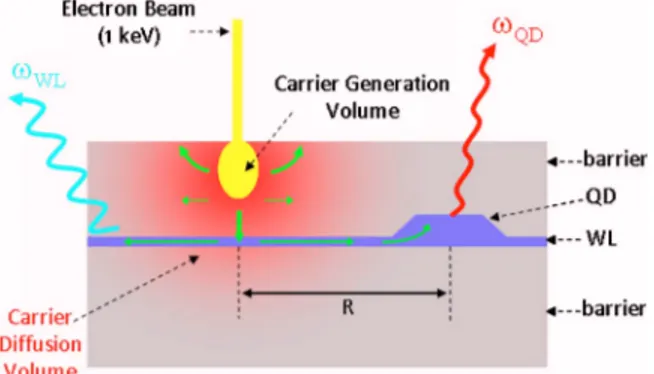
Figure1shows the schematic of the experiment. A low-voltage electron beam generates excess carriers in the barrier layer just below the surface of the QD structure. Most of them relax very rapidly into the WL in the picosecond range,12 then diffuse through it,13 and finally get captured into the QDs where they can recombine and emit light. Other carriers are either captured by surface defects near the beam impact or recombine in the barrier and WL. So, we can as-sume that carrier diffusion takes place mainly in the WL when the scanning electron beam is far from the dot. Fur-thermore, the density of electron-hole pairs generated in this confined region close to the surface is very high and much greater than the barrier majority carrier concentration. Thus, only ambipolar diffusion lengths of excess carriers in the WL can be determined. The diffusion length is deduced from CL intensity profile I共R兲 over the QD with R as the distance between the probe and the QD.
a兲Present address: CEA/Grenoble-INAC/SP2M/SiNaPS, 17 rue des Martyrs, 38054 Grenoble Cedex 9, France.
b兲Author to whom correspondence should be addressed. Electronic mail: [email protected].
FIG. 1. 共Color online兲 Schematic of the experiment. Excess carriers gener-ated in sub-10-nm volume of the barrier are mainly captured by the WL and diffuse through it before their final capture into a QD. Diffusion length is deduced from CL intensity profile I共R兲 over the QD.
APPLIED PHYSICS LETTERS 94, 022113共2009兲
The investigated structure is made of InAs self-assembled QDs grown by solid-source molecular beam epi-taxy on a semi-insulating InP共001兲 substrate.14
In order to spatially resolve QD luminescence, a specific growth proce-dure was implemented to produce diluted QDs,15whose den-sity is reduced to about 1 QD/m2. The resulting dots are
truncated pyramids with a typical lateral size of 30–40 nm and height of 2–5 nm. The InAs WL below the QDs has a mean thickness of 2 ML. QDs are capped with a thin 20 nm InP layer to allow excess carriers generated near the surface to reach the WL region. CL measurements were performed in a Zeiss Supra 55 VP field emission scanning electron micro-scope equipped with a continuous helium flow cryostat pro-viding temperature from 5 to 300 K. The luminescence was dispersed by a 30 cm grating monochromator and detected by a cooled InGaAs cathode photomultiplier tube within the 0.3– 1.65 m spectral range. CL micrographs were per-formed using a long pass cutoff filter at 1.1 m and a 1 kV focused electron beam at several probe currents 共Ib兲. At 1 kV, p is about 3 nm and according to Monte Carlo simulations,16electron-hole pairs are injected into sub-10-nm volumes in the InP barrier providing a quasipoint source of carriers.
Figure2shows a CL image of such an array of InAs/InP QDs obtained at 1 kV, 300 K, and for Ib= 3 nA. The bright spots are correlated with the emission of individual dots. This has been confirmed by observing complementary fea-tures on WL and QD CL images of the same area at low temperatures and by comparing the density of bright spots with QD density estimated by AFM measurements on an uncapped sample. The measured spectrum of the same sample is presented共inset兲. We can clearly see the WL emis-sion around 1 m and the QD emission starting at 1.1 m and extending up to 1.65 m. The dashed area on the image represents the wavelength range removed using the optical filter.
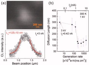
Figure 3共a兲shows the CL image over a specific region obtained at higher magnification and its related CL intensity profile for Ib= 3 nA. When the electron beam is scanned above one QD, the CL signal is nearly constant since carriers are captured efficiently into this dot. For an excitation spot away from the dot, the CL signal decreases since part of the
excess carriers recombine in the WL. For ambipolar diffu-sion of carriers, the local density of electrons and holes is obtained by solving the continuity equation under a steady state regime. If we assume that dots act as perfect sinks, the diffusion current will be more pronounced toward the nearest dot direction. A one-dimensional diffusion equation can then be used to obtain the approximate distribution of carriers from the generated point at r = 0 to the dot position at r = R. This is a well known diffusion problem with trivial limit conditions at r = 0, diffusion current equals generation rate, and at r = R, carrier density in the WL is zero. The carrier diffusion current evaluated at the dot position is given by I共R兲⬀csch共R/La兲, where La is the ambipolar diffusion length. This expression is valid for RⰇp, Re, r0, the QD
radius. We assume that the QD CL signal is linearly propor-tional to this diffusion current at r = R. The mean Lavalue is then obtained through the fit of 15 CL intensity profiles across isolated bright spots taken randomly at different sample areas. Figure 3共b兲 presents mean carrier diffusion length values as a function of probe current and carrier gen-eration rate at 300 K. For the lowest carrier injection at 3 kV and Ib= 0 , 42 nA, we found 300⫾50 nm, which is in accor-dance with another group value17 taken at low-level injec-tion. It decreases down to 120⫾30 nm and then slightly increases at higher injections. Enhanced nonradiative carrier recombination by Auger processes in the WL is suggested as an explanation for the reduced diffusion length observed at higher excitation current. The slight increase might be attrib-uted to enhanced carrier diffusion into the InP barrier as the WL state filling becomes more important. One can note that the calculated standard deviation 共⌬La= 50 nm兲 is much larger than the mean deviation in the lateral size of our QD ensemble共about 15 nm兲. This high ⌬La value suggests that there exist local carrier transport inhomogeneities in the WL, most probably resulting from interface roughness, InAsxP共1−x兲 alloy composition and strain induced QD size effects. Ambipolar diffusion length is related to the carrier mobility by this La=
冑
kBT/e expression, where is the carrier lifetime in a WL in the absence of QDs共recombina-FIG. 2. CL intensity micrograph of a low QD density InAs/InP sample, acquired at 1 kV and 300 K using a long pass filter cutoff at 1.1 m. The luminescence on the map corresponds to the QDs emitting between 1.1 and 1.65 m as shown by the CL spectrum共inset兲.
FIG. 3. 共Color online兲 共a兲 Zoom on a submicrometer bright spot associated with a single QD and its CL intensity profile at 300 K for Ib= 3 nA. The
ambipolar diffusion length Lais deduced from the csch共R/L兲 fitting curves
共solid line兲. 共b兲 Lavalues as a function of beam intensity and carrier
gen-eration rate at 1 kV and 300 K. One measure is made at 3 kV and 0.42 nA as indicated. Error bars correspond to the calculated mean standard deviation.
tion in the dot is taken into account in the boundary condi-tion兲. From low-excitation density time-resolved photolumi-nescence measurements, Raymond et al.18 determined a value of about 330 ps in an ultrathin InAs quantum well, comparable in thickness to our WL. If we consider this value for the 300 nm La measurement obtained at 300 K, we obtain an ambipolar mobility value of about 110⫾10 cm2/共V s兲. By assuming the same carrier mobility as we increase the current to 3 nA, we obtain from the mea-sured La value a limited Auger recombination lifetime of about 50 ps.
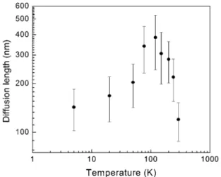
Mean carrier diffusion lengths have also been measured between 5 and 300 K for Ib= 3 nA 共Fig. 4兲. The La value increases from 120 to 390 nm between 300 and 120 K and then decreases down to 140 nm at 5 K. The carrier mobility also peaks around 100 K in III-V semiconductor quantum wells.19,20 Moreover, the carrier lifetime in a thin quantum well is expected to be nearly constant at low temperatures 共T⬍120 K兲 and to decrease at higher temperatures due to thermal activation of the carriers and recombination into the InP barrier. We thus obtain a fair qualitative agreement with the expected La共T兲 function. It is important to emphasize the fact that the diffusion length increases by only a factor of 3 between 5 and 100 K, whereas an enhancement of 42 ⬇共100/5兲5/4 is expected if carrier scattering by ionized
im-purities limits the mobility in this temperature range. Our results indicate that interface roughnesses and alloy compo-sition fluctuations play a key role in limiting the carrier mo-bility in an ultrathin WL
In conclusion, we investigated the transport properties of excess carriers in the WL of a diluted InAs QD structure using low-voltage CL imaging with submicron spatial
reso-lution. This method provides a direct measurement of the carrier diffusion length in the WL. An ambipolar carrier mo-bility of about 110 cm2/共V s兲 is estimated from the 300 K
La value. The T-dependence of the diffusion length is diffi-cult to model but our results give valuable insights on pos-sible scattering mechanisms in this InAs/InP system.
This work was partly supported by Canadian grant funds 共NSERC, FQRNT, and Nano-Québec兲 and by the program Frontenac, which supports France/Québec exchange gradu-ate students. E.D. would like to thank Jean Beerens, Pierre Lafrance, and Marcel Zakorzermy for their technical support.
1J. Wang, U. A. Griesinger, and H. Schweizer,Appl. Phys. Lett. 69, 1585 共1996兲.
2M. Ono, K. Matsuda, T. Saiki, K. Nishi, T. Mukaiyama, and M. Kuwata-Gonokami,Jpn. J. Appl. Phys., Part 2 38, L1460共1999兲.
3V. Zwiller, M. Pistol, D. Hessman, R. Coderstrom, W. Seifert, and L. Samuelson,Phys. Rev. B 59, 5021共1999兲.
4M. Merano, S. Sonderegger, A. Crottini, S. Collin, P. Renucci, E. Peluc-chi, A. Malko, M. H. Baier, E. Kapon, B. Deveaud, and J. D. Ganiere, Nature共London兲 438, 479共2005兲.
5A. Gustafsson, M. E. Pistol, L. Montelius, and L. Samuelson,J. Appl. Phys. 84, 1715共1998兲, and references therein.
6H. A. Zarem, P. C. Sercel, J. A. Lebens, L. E. Eng, A. Yariv, and K. J. Vahala,Appl. Phys. Lett. 55, 1647共1989兲.
7N. M. Haegel, J. D. Fabbri, and M. P. Coleman, Appl. Phys. Lett. 84, 1329共2004兲.
8A. Fiore, M. Rossetti, B. Alloing, C. Paranthoen, J. X. Chen, L. Geelhaar, and H. Riechert,Phys. Rev. B 70, 205311共2004兲.
9D. P. Popescu, P. G. Eliseev, A. Stintz, and K. J. Malloy,J. Appl. Phys.
94, 2454共2003兲.
10A. F. G. Monte, F. V. de Sales, S. W. da Silva, M. A. G. Soler, J. M. R. Cruz, P. C. Morais, M. J. da Silva, A. A. Quivy, and J. R. Leite,Physica E共Amsterdam兲 17, 122共2003兲.
11V. I. Petrov, Bull. Acad. Sci. USSR, Phys. Ser.共Engl. Transl.兲 56, 287 共1992兲.
12J. Siegert, S. Marcinkevičius, and Q. X. Zhao,Phys. Rev. B 72, 085316 共2005兲.
13D. Araújo, G. Olegart, J.-D. Ganière, and F.-K. Reinhart,J. Appl. Phys.
76, 342共1994兲.
14E. Dupuy, P. Regreny, Y. Robach, M. Gendry, N. Chauvin, E. Tranvouez, G. Bremond, C. Bru-Chevallier, and G. Patriarche,Appl. Phys. Lett. 89,
123112共2006兲.
15E. Dupuy, Proceedings of the 20th International Conference on Indium Phosphide and Related Materials, Versailles, France, 25–29 May 2008 共unpublished兲.
16For the simulations of the primary electron trajectories in solids, we used theCASINOsoftware: http://www.gel.usherb.ca/casino. For more informa-tion, see D. Drouin, A. Real-Couture, D. Joly, X. Tastet, V. Aimez, and R. Gauvin, Scanning 29, 92共2007兲
17A. Gustafsson, D. Hessman, L. Samuelson, J. F. Carlin, R. Houdré, and A. Rudra,J. Cryst. Growth 147, 27共1995兲.
18S. Raymond, K. Hinzer, S. Fafard, and J. L. Merz, Phys. Rev. B 61, R16331共2000兲.
19H. Hillmer, A. Forchel, S. Hansmann, M. Morohashi, E. Lopez, H. P. Meier, and K. Ploog,Phys. Rev. B 39, 10901共1989兲.
20L.-L. Chao, G. S. Cargill III, E. Snoeks, T. Marshall, J. Petruzzello, and M. Pashley,Appl. Phys. Lett. 74, 741共1999兲.
FIG. 4. Temperature dependence of carrier diffusion length before QD cap-ture for Ib= 3 nA. Error bars correspond to the mean standard deviation.