UNIVERSITÉ DU QUÉBEC À MONTRÉAL
ON THE INTEGRATION OF CHROMOPHORES WITH
MULTIDIRECTIONAL CHARGE-TRANSFER WITH SILICON
W A VEGUIDES FOR NONLINEAR APPLICATIONS
MASTER
'
S THESIS
PRESENTED
AS A PARTIAL REQUIREMENT
FOR THE MASTER'S DEGREE IN ELECTRICAL ENGINEERING
BY
MONIR DELA V ARI
Avertissement
La diffusion de ce mémoire se fait dans le respect des droits de son auteur, qui a signé le formulaire Autorisation de reproduire et de diffuser un travail de recherche de cycles supérieurs (SDU-522 - Rév.0?-2011 ). Cette autorisation stipule que «conformément à l'article 11 du Règlement no 8 des études de cycles supérieurs, [l'auteur] concède à l'Université du Québec à Montréal une licence non exclusive d'utilisation et de publication de la totalité ou d'une partie importante de [son] travail de recherche pour des fins pédagogiques et non commerciales. Plus précisément, [l'auteur] autorise l'Université du Québec à Montréal à reproduire, diffuser, prêter, distribuer ou vendre des copies de [son] travail de recherche à des fins non commerciales sur quelque support que ce soit, y compris l'Internet. Cette licence et cette autorisation n'entraînent pas une renonciation de [la] part [de l'auteur] à [ses] droits moraux ni à [ses] droits de propriété intellectuelle. Sauf entente contraire, [l'auteur] conserve la liberté de diffuser et de commercialiser ou non ce travail dont [il] possède un exemplaire."
UNIVERSITÉ DU QUÉBEC À MONTRÉAL
ÉTUDE SUR L'INTEGRATION DE CHROMOPHORES
À
TRANSFERT DE CHARGES MULTIDIRECTIONNEL AVEC DES
GUIDES D'ONDE EN SILICIUM POUR DES APPLICATIONS
NON-LINÉAIRES
MÉMOIRE
PRÉSENTÉ
COMME EXIGENCE PARTIELLE
DE LA MAÎTRISE EN GÉNIE ÉLECTRIQUE
PAR
MONIR DELA V ARI
LIST OF TABLES ... X LIST OF ABBREVIA TI ONS ... Xl ABSTRACT ... XIV RÉSUMÉ ... XV CHAPTERI
THE RESEARCH PROBLEM............................................. ... 1
1.1 Optical Communication Systems ... 1
1.2 Silicon Photonics ... 3
1.3 Optical Slot Waveguides with Nonlinear Chromophores .... 5
1.4 Thesis Objectives ... 7
1.5 Thesis Outline ... 9
CHAPTERII THEORETICAL BACKGROUNDG ............................ 11
2.1 Nonlinear Optics in Waveguides ... 11
2.1.1 Maxwell's Equations and Nonlinear Polarization... ... Il 2.1.2 Optical Waveguides and Propagating Modes ... 13
2.1.3 [deal Waveguide Mode Analysis ... 15
2.1.4 Modes in 3-D Waveguides ... 17
2.1.5 Bearn Propagation Method (BPM) Technique ... 18
2.1.6 Third-order Nonlinear Interaction ... 20
2.2 Nonlinear Parameters ... 21 2.3 Couple-Mode Theory ofFour-Wave Mixing ... 23
2.3.1 Origin of Four Wave Mixing ... 23
2.3.2 Coup led-Mode The01·y ... 24
2.3.2.1 Wavelength Conversion ... 25
v
2.4 Nonlinear Optical Slot Waveguides.· ... 27
2.5 Multidirectional Charge-Transfer Transitions Molecules ... 32
2.5.1 Molecular Hyperpolarizability ... 33
2.5.2 Third-Order Nonlinear Chromophores ... 34
CHAPTERID MATERIALS AND FABRICATION ... 35
3.1 Materials ... 35
3.1.1 PMMA ... 35
3.1.2 Crystal Violet ... 36
3.2 Silicon Slot Waveguides ... 37
3.2.1 Waveguide Design ... 3 7 3.2.2 Deviee Fabrication ... 42
3.2.3 Deposition of Crystal Violet. ... 45
CHAPTERIV THIRD-ORDER NONLINEAR EFFECT IN SOI W A VEGUIDES ...... 51
4.1 Numerical Calculations of Slot Waveguide Modes ... 51
4.2 Effective Area of the Third-order Nonlinear Interaction .... 56
4.3 Dispersion and Phase-matching Condition ... 58
4.4 Nonlinear Parameters of Crystal Violet ... 60
4.4 .1 Third Order N onlinear Susceptibil ity ... 60
4.4 .2 N onlinear Waveguide Parameter. ... 61
4.5 FWM-based Wavelength Conversion ... 63
CHAPTERV EXPERIMENTAL SETUP AND MEASURMENTS .... 67
5.1 Experimental Setup and Measurements ... 67
5 .1.1 Propagation Loss Measurements ... 69
5.2 FWM-based Wavelength Conversion Experiment.. ... 76
CHAPTERVI
CONCLUSION ... 79 REFERENCE ... 83
LIST OF FIGURES
Figure 1.1: Two-photon absorption mechanism (adapted from (Paschotta, 2008))
...•...•.... 4
Figure 1.2: Schematic of a slot waveguide using nonlinearities in the slot (From
(Leuthold, Koos and Freude, 2010)) ... 6
Figure 2.1: Basis structure of a slab waveguide (From (Okamoto, 2010)) ... 14
Figure 2.2: The refractive indices of a strip waveguide. (From (Okamoto, 2010)
... 14
Figure 2.3: Schematic of a slot waveguide using nonlinearities in the slot (From
(Leu tho Id, Koos and Freude, 201 0)) ... 17
Figure 2.4: Schematic of a slot waveguide. The TE-mode (shown in orange) is
confined in the low-index slot region [From (Anderson, Schmidt and Lipson,
2006)] ... 28
Figure 2.5: Cross-section of waveguides a) Strip waveguide (core and cover
nonlinearity) b) slot waveguide (cover nonlinearity) [From (Leuthold et. aL, 2009)] ... 29
Figure 2.6: Molecular structure of p-nitroaniline with unidirectional charge
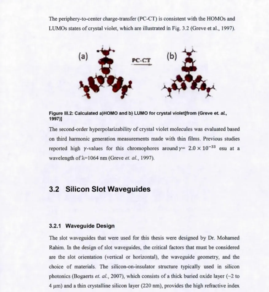
Figure 3.1: Molecular structure of crystal violet [from (Greve et. lli., 1997)) ... 36
Figure 3.2: Calculated a)HOMO and b) LUMO for crystal violet[from (Greve et. al, 1997)) ... 37
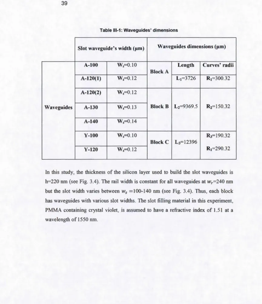
Figure 3.3: Top-view SEM picture of design. The letters refer to Table 3.1. ... 38
Figure 3.4: Slot waveguide structure ... 40
Figure 3.5: Top-view SEM picture of the Y -branch ... 40
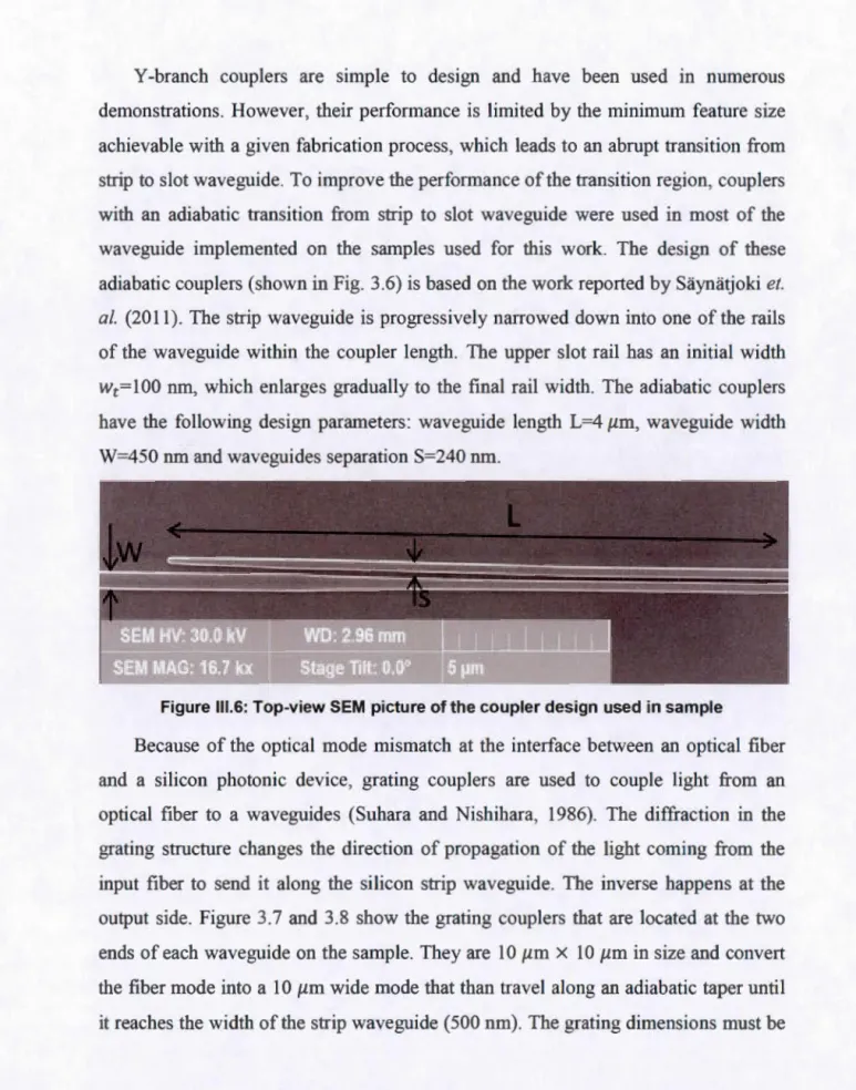
Figure 3.6: Top-view SEM picture of the coupler design used in sample ... 41
Figure 3.7: Top-view SEM picture of grating coupler ... 42
Figure 3.8: Image of the grating couplers at the end of one block of waveguides ... 42
Figure 3.9: Cross-section of SiPhotonics Standard Passives (PSV) FC and WG modules (Dumon, 2012) ... 43
Figure 3.10: Cross-section of SiPhotonics PSV with resist cladding (Dumon, 2012) ... 44
Figure 3.11: Sample covered with crystal violet 5 wt % dissolved in chlorobenzene ... 46
Figure 3.12: Sample covered with crystal violet 5 wt. % dissolved in chloroform ... 47
Figure 3.13: SEM picture of the cleaved sample deposited with 5 wt. % PMMA ... 48
IX
Figure 3.14: SEM picture of the cleaved sample deposited with 1 wt. % crystal
violet ... 48
Figure 4.1: Counter map of transverse index profile of a slot waveguide with
crystal violet cladding. The colour scale represents the refractive index value .. 52
Figure 4.2: Top-view SEM picture of the slot waveguide ... 53
Figure 4.3: Normalized transverse E-field profile of the quasi-TE mode for
ncover=l.51 for a) w5=100 nm b) w5=120 nm c) w5=130 nm d) w5=140 nm. The
co lor scale shows the electric field normalised amplitude ... 54
Figure 4.4: Effective refractive index of crystal violet as a function of wavelength
for for various slot widths 100 nm<w5<140 nm ... 55
Figure 4.5: Horizontal eut of the Ex mode profile at Y=O ... 56
Figure 4.6: Effective area AefT for various slot widths 100 nm<w5<140 nm as a
function of the cladding refractive index ... 58
Figure 4.7: Simulated GVD for the TE mode as a function of wavelength for
W5=140 nm ... 59 Figure 4.8: Third order nonlinear susceptibility for a polymer film doped with
10 wt. % crystal violet as a function of wavelength (adapted from Ramos-Ortiz
et al., 2007) ... 61
Figure 4.9: Theoretical conversion efficiency as a function of idler wavelength
for slot waveguides filled with crystal violet 10 wt. % for slot widths 100 nm<
Figure 4.10: Theoretical conversion efficiency as a function of idler wavelength
for a silicon channel waveguide ... 65 Figure 4.11: Theoretical conversion efficiency as a function of idler wavelength
for slot waveguides with an input power of Pin=300 rn W ... 66 Figure 4.12: Theoretical conversion efficiency as a function of idler wavelength
for silicon waveguide with an input power of Pin=300 rn W ... 66
Figure 5.1: Schematic of a grating coupler used to couple light into a photonic
integrated circuit (adapted from (Pello, 2014)) ... 67 Figure 5.2: Loss measurement setup ... 68 Figure 5.3: Measurement of the insertion loss for the fundamental TE mode for
slot waveguides with a slot width ofws=140 nm and cladded with 5 wt% PMMA
dissolved in chlorobenzene ... 71 Figure 5.4: Expected conversion efficiency for slot waveguide with slot width of ws= 140 nm filled with 1 wt. % crystal violet ... 75
Figure 5.5: FWM experimental setup: ECL: External cavity laser; EDFA: Erbium doped fiber amplifier; PC: Polarization controller; OSA: Optical
LIST OF TABLES
Table 2-1: Cladding nonlinearity for inorganic materials (adapted from (Koos
et. al., 2007)) ... 30
Table 2-2: Cladding nonlinearity for organic materials (adapted from (Koos et.
aL, 2007)) ... 31
Table 3-1: Waveguides' dimensions ... 39
Table 3-2: Overview of process modules ... 44
Table 4-1: Effective refractive index of crystal violet for different slot width .... 55
Table 4-2: Summary of material parameters and nonlinear coefficients for
crystal violet ... 62
Table 4-3: Nonlinear parameter and nonlinear effective area for different slot
widths ... 62
Table 5-1: Measurements of insertion tosses, propagation tosses and coupling
tosses for waveguides ftlled with PMMA 5 wt. % dissolved in chlorobenzene .... 72
Table 5-2: Measurements of insertion tosses, propagation tosses and coupling
tosses for waveguides filled with PMMA 5 wt. % dissolved in chloroform ... 73
Table 5-3: Measurements of insertion tosses, propagation tosses and coupling
Aeff CT
cv
cw
BPM DANS DFWM DI DUV ECL EDFA FC FCA FDTD FEFDEffective modal area
Charge transfer
tris( 4-N N-dimethylamino phenyl)methyl
(Crystal violet) Continuous wave
Bearn Propagation Method
4-dialkyamino-4' nitro-sti lbene
Degenerate four-wave mixing
De-ionized
Interaction domain
deep ultraviolet
Externat cavity laser
Erbium-doped fiber amplifier Fiber coupler
Free-carrier absorption
Finite-difference Time-domain
Xlii FWM GVD HOMO IR LOMO mW lleff OSA PC PC-CT PDA PMMA PSV PIA PTS RESCLAD SEM Si Si02 SOI SPM Four-wave mixing
Group velocity dispersion
Highest occupied molecular orbital
Infrared
Lowest unoccupied molecular orbital
Milliwatt
Effective refractive index
Optical spectrum analyser
Polarization controller
periphery-to-center charge-transfer
Polydiacetylene
Poly (methyl methacrylate)
Passive
polytriactelyene
poly(p-toluene sulphonate)
Resist cladding
Scanning electron microscopy
Silicon
Silicon dioxide
Silicon on insulator
Tbs·' Terabit per second
TE Transverse electric
TEE tetraethynylethene
TM Transverse magnetic
TIR Total internai reflection
TPA Two-photon absorption
WG Waveguide
ABSTRACT
SOI-based nonlinear slot waveguides cladded with crystal violet are of great interest for ultrafast all-optical signal processing. In this work, the optical properties of slot waveguides filled with crystal violet were investigated experimentally and their nonlinear potential was studied numerically.
This thesis covers the theoretical basics of nonlinear optics, slot waveguide design, deviee fabrication, a simulation study of the four-wave mixing conversion efficiency in slot waveguides filled with crystal violet, the challenges of using crystal violet in the cladding of silicon photonic deviees, a deposition process for crystal violet chromophores in a PMMA host on silicon slot waveguides, and experimental demonstrations and characterisation of the propagation lasses of slot waveguides filled with a polymer containing crystal violet chromophores.
The dispersion profile, the effective mode area and the nonlinear parameters of slot waveguides were estimated by using a MATLAB script. The slot waveguide geometry and design were optimized to give an effective core area of 0.321 11m2, leading to a nonlinear coefficient of 394 (Wmr1for a slot width of 140 mn for the fundamental TE mode. A combination of standard photolithography and etching was used to fabricate the waveguides with the desired dimensions. The linear characterization of these slot waveguides cladded with crystal violet shows that the lowest linear loss achieved to date is approximately 11 dB/cm.
This study prepared the foundation for the development of a novel category of highly nonlinear hybrid silicon deviees tbat exploit the unique design and optirnization opportunities made possible by chromophores relying on multi-charge transfer transitions.
Keywords: Slot-waveguides, Nonlinear chromophore, Third arder Nonlinear effect, Conversion efficiency
Les guides d'onde à rainure non linéaire ayant une gaine contenant du cristal violet sont d'un grand intérêt pour le traitement tout-optique ultra-rapide de signaux lumineux. Dans ce mémoire, les propriétés optiques de guides d'onde à rainure remplis avec du cristal violet ont été étudiées expérimentalement et leur potentiel non linéaire a été étudié numériquement.
Ce mémoire couvre les bases théoriques de l'optique non linéaire, la conception de guide d'ondes à rainure, leur fabrication, une étude par simulation de l'efficacité du mélange à quatre ondes dans des guides d'onde à rainure remplies de cristal violet, les défis de l'utilisation du cristal violet dans la gaine de dispositifs photoniques en silicium, un procédé de dépôt pour les chromophores de cristal violet dans un hôte de PMMA sur des guides d'onde à rainure en silicium et des démonstrations expérimentales et la caractérisation des pertes de propagation des guides d'ondes à rainure remplis d'un polymère contenant des chromophores de cristal violet.
La dispersion, la surface effective du mode et les paramètres non linéaires des guides d'ondes à rainure ont été estimés en utilisant un script de simulation fonctionnant avec MA TLAB. La géométrie des guides d'onde à rainure a été optimisée pour obtenir une surface effective de 0,321 um2, ce qui produit un coefficient non linéaire de 394 (Wm)-1pour une largeur de rainure de 140 nm pour le mode TE fondamental. Une combinaison de photolithographie et de gravure sèche a été utilisée pour fabriquer des guides d'onde avec les dimensions désirées. La caractérisation de ces guides d'onde à rainure ayant une gaine de cristal violet montre que la plus faible perte linéaire réalisée à ce jour avec ce type de guide d'onde est d'environ 11 dB
1
cm.Cette étude a jeté les bases pour le développement d'une nouvelle catégorie de dispositifs hybrides fortement non linéaires qui exploitent les possibilités de conception et d'optimisation uniques des chromophores possédant plusieurs transitions de transfert de charge.
Mot de clés : Guides d'onde à rainure, Chromophore non linéaire, Effet non linéaire du troisième ordre, Efficacité de conversion
CHAPTERI
THE RESEARCH PROBLEM
Over the past few years, highly nonlinear silicon waveguides have been developed in order to increase the flexibility of optical networks. They achieve this by enabling all-optical processing, which can handle enorrnous bandwidth and can be transparent to modulation fonnats. Silicon nanowaveguides have been optimized to enhance nonlinear effects such as four-wave mixing (FWM). Furthermore, they have demonstrated great potential for wavelength conversion (Ophir et. al., 2012; Xu et.
al., 2011). However, there are important limitations to the conversion efficiency that
can be achieved with silicon waveguides, such as the losses caused by two-photon absorption at telecommunication bandwidths, or the significant input power (> 1 OOm W) that must be coup led into them to observe nonlinear effects. Thus, ways to reduce the impact of these limitations must be investigated to be able to perfonn all-optical signal processing by taking advantage of ultrafast xC3)_nonlinearities and the large optical bandwidth of silicon waveguides.
In this chapter, the growth of the optical communication field is discussed, and the potential of integrated silicon photonics as a solution to overcome the challenges posed by high data rates is presented. Finally, the objectives and the organization of this thesis are described.
1.1 Optical Communication Systems
Recently, optical communication systems have gathered a lot of attention and tremendous work bas been done, especially to mcrease their transmission rate. Moreover, the large bandwidth available in optical fibers can be used to create optical links with transmission rates of more than 1 Tbs-1 on a single fiber by using
wavelength division multiplexing and these signais can be sent across hundreds of kilometers.
Furthermore, the continuation of Moore's law (Moore, 1998), which states that the nwnber of transistors on an electronic integrated circuit should double every two years, has caused an exponential increase in computing power. As a result, transmission systems with large bandwidth are required to transport and utilize the tremendous amounts of data that is produced. Accordingly, advancements in the fields of optics and microfabrication have enabled the development of a vast number of integrated optical deviees that make possible the creation of high capacity data links. Hence, integrated optic plays a crucial role in the optical fiber networks that form the backbone of the Internet (Levy, 2011 ).
The demand for higher data rates and reduced power consumption means that optics hold distinct advantages over electronics (Preston, 2011). For example, in electrical connections the signal attenuation with distance is very high (Gambling, 2000) but optical networks can provide significantly larger bandwidth, lower power consumption per bits and have practically no distance limitations. However, the cost of optical transceivers bas always been an issue but this could be overcome thanks to integrated photonic deviees that can be fabricated cheaply by taking advantages of the new developments and techniques in microfabrication processes (Paniccia, Krutul et. Koehl, 2004). Also, to build optical systems, the alignment of the optical components must be done accurately, which requires sophisticated packaging techniques. The development of advanced optical networks and the replacement of large optical sub-systems by chip-scale deviees make the improvement of integrated photonics crucial. Since ultrafast nonlinear optical effects can be employed to process signais at frequencies exceeding the THz, all-optical signal processing has the potential to enable photonic deviees operating at Tbit/s line rates (Igarashi et Kikuchi, 2008; Willner et al., 2011 ). Moreover, because telecommunication networks rely more and more on optical signals, an effective and low-cost technology is needed to build all-optical signal processing components that can ensure that system speed and capacity
3
continue to increase. Thus, the increasing demand for high-speed and reconfigurable optical networks requires the study of optical signal processing. lntegrated photonics can perform all-optical data signal processing at decreased costs. For instance, FWM is a nonlinear effect that bas proven useful to create all-optical signal processing components, such as wavelength conversion deviees (Lin et. al., 2006) that could be used to resolve contention problems.
1.2 Silicon Photonics
Various low-index-contrast material systems, such as doped silicon dioxide (Si02) and polymers (Foresi et. al., 1997; Kuwata-Gonokami et. al., 1995 ; Little et.
al., 2004), have been used to fabricate optical waveguides and integrated photonic
deviees over the past decade. However, lately bigb-index-contrast material systems, such as silicon (Si) and III-V compounds (Masanovic et. al., 2005; Soltani, Y egnanarayanan et. Adibi, 2007 ; Vlasov et. al., 2005), have gained more attention because they can provide bigb optical confinement, which make possible bigh levels of integration and can increase optical power densities. Among higb-index-contrast material platforms, silicon-on-insulator (SOI) is the most used for photonic applications because of its cost advantages and of the advanced fabrication processes that are commercially available.
Silicon pbotonics bas been a rapidly growing field of researcb because of the increasing accessibility of bigb-quality silicon-on-insulator (SOI) wafers (Celler and Cristoloveanu, 2003) wbere a layer of silicon oxide separates a layer of single-crystal silicon from the bulk handle wafer. Important functionalities were demonstrated on this platform. For example, many important components can be fabricated on a silicon photonic chip such as: photodetectors (Assefa, Xia and Vlasov, 201 0; Kang et. al., 2009), hybrid laser sources (Fang et. al., 2006), filters (Dong et. al., 2010; Xia et. al., 2007) and modula tors (Reed et. al., 20 l 0). Thus, silicon photonics bas enabled the integration of numero us components on a single chi p.
By usmg silicon, which has a high refractive index (n~3.48) at telecommunication wavelength (À= 1550 nm), it is possible to obtain a strong confinement of the optical modes. Silicon possess a high nonlinear refractive index, n2, in the range of (4-9)x 10"14 cm2W"1 (Dinu, Quochi and Garcia, 2003 ; Fukuda et. al., 2005 ; Tsang et. al., 2002), which is three orders of magnitude larger than silica glass. Moreover, the tight modal confinement in SOI waveguides bas a great impact on the nonlinear parameter since it is inversely proportional to the effective area of the mode, y
ex:
nz!Aetf (Foster et. al., 2006). Although silicon has been the core material used in the microelectronics industry due to its versatility and cast, it bas some important drawbacks for nonlinear optics. For example, its energy gap is 1.12e V, and th us, at telecommunication wavelengths two-photon absorption appears because the bandgap is less that the energy of two photons at these wavelengths. Furthennore, two-photon absorption (TP A) in duces !osses thatare
cornpounded by the carriers generated, which produce free carrier absorption (FCA). In the TPA process (see Fig. 1.1) an electron makes a transition from the valence band to the conduction band of silicon by the simultaneous absorption of two laser photons, which increases the concentration of free charges. Therefore, the combination of TPA and FCA limits the efficiency of nonlinear processes at telecommunication wavelengths in silicon excitation with two photons conduction band ele-ctron wavenumber k5
More generally, the causes behind the challenges of using silicon in integrated optics are as follows: ( 1) the indirect minimum-energy bandgap, which leads to inefficient stimulated emission and impractical laser action; (2) the centrosymmetry of silicon crystal, which limits the electro-optic effects used for active deviees such as modulators; and (3) at telecommunication wavelengths, silicon bas a large
two-photon absorption coefficient that affects the third-order nonlinear effects (Leuthold, Koos et. Freude, 2010). For these reasons, it is desirable to use more efficient materials and combine them with a silicon structure for certain on-chip functions. This is the motivation behind the work presented in this thesis, which investigates the development of novel hybrid silicon waveguides that could enable nonlinear applications.
1.3 Optical Slot Waveguides with Nonlinear
Chromophores
As mentioned in the previous section, despite the obvious advantages of using silicon to build deviees for optical telecommunication systems, it bas severe limitations for a few functionalities, in particular those relying on nonlinear effects. Moreover, its high refractive index makes it difficult to couple light efficiently to cladding materials because of the high confinement it provides. Nevertheless, it is possible to achieve a
very high level of interaction with a cladding material by using a 'slot waveguide' structure. One can then work with a highly nonlinear cladding material with low two-photon absorption and benefit from a high leve! of optical confmement in the slot reg1on.
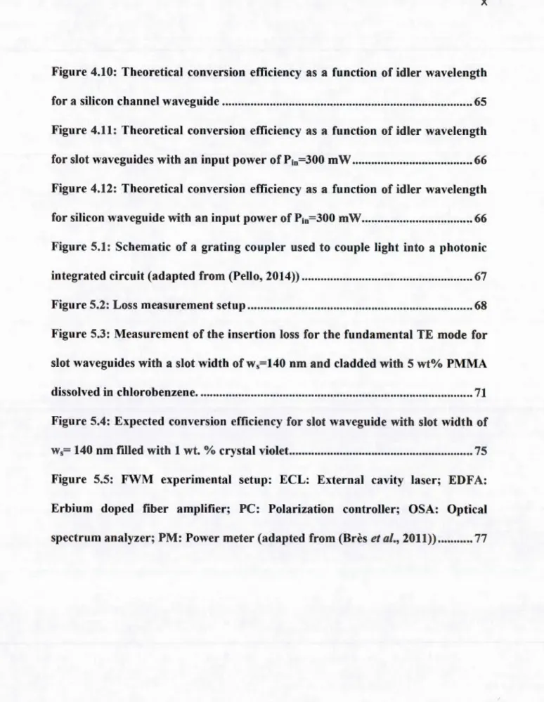
The silicon slot waveguide structure was developed to generate an intense optical mode in the low index region of the waveguide (see Fig 1.2). This structure is made of two channel waveguides with a high refractive index core ma teri al that are brought
in close proximity to forma narrow law index slot region in which most of the optical power will be confined (Almeida et. al., 2004).
Slot nonhnearity
1 •1avegu•de
S10 TE
Figure 1.2: Schematic of a slot waveguide using nonlinearities in the slot (From (Leuthold, Koos and Freude, 201 0))
The slot waveguide structure functions as a result of the electric field discontinuity at the high-index contrast barrier between the silicon core and the cladding. As a result, the electric field is more intense in the slot region than in the silicon waveguides. Furthermore, the slot waveguides can be used for various functionalities, such as light emission, electro optic modulators (Baehr-Jones et. al., 2008), amplification, and waveguides with ultrafast nonlinearity and supressed free-carrier effects (Koos et. al., 2009) because of the strong electric field enhancement in the slot region and that this slot can be filled with a variety of law-index materials (Almeida et. al., 2004; Xu et. al., 2004).
To fill the law-index slot region, the nonlinear optical chromophore tris(4-N,N-dimethylaminopheny 1 )methyl ( also known as 'crystal violet') which has a high second-arder hyperpolarizability y and display multi-charge transfer transitions, was chosen for this study. It was demonstrated experimentally that the high second-arder hyperpolarizability, y, provided by the molecular structure of crystal violet within the range of wavelengths used in optical telecommunication originates from the conjugated and highly polarized rr-electron backbone (Bosshard et. al., 1996 ; Greve et. al., 1997). Thus, octupolar chromophores with three-fold symmetry and
multi-7
charge transfer transitions, such as crystal violet, provide higher hyperpolarizability and they show multiple donor-acceptor substituents due to the chromophore units, polymer backbone, and their molecular symmetry that helps to have a mu! tidirectional charge transfer.
Silicon slot waveguides with a nonlinear cladding material have demonstrated a small effective mode area (Aett) and a high nonlinear parameter (y) that make them suitable to build wavelength converters with high conversion efficiency (Liu et. al., 2011 ). In FWM -based wavelength conversion, the conversion bandwidth and the efficiency are closely related to the phase-matching condition, which can be optirnized by engineering the dispersion profile of the waveguides (Gao, Li and Zhang, 201 0). In this work, for the first time, crystal violet, which displays periphery-to-center charge-transfer transitions, is used as the cladding material in slot waveguide structures. We analyze the nonlinear parameters of slot waveguides filled with crystal violet as a function of their geometry, which impacts the effective mode area and the waveguide dispersion profile. Based on the optimized slot waveguide configuration, the FWM conversion efficiency has been studied numerically. Furthermore, the integration challenges of polymers containing crystal violet molecules with silicon slot waveguides were investigated experimentally.
1.4 Thesis Objectives
Various nonlinear polymers have been used as cladding material to fil! slot waveguides (Koos et. al., 2009). However, nonlinear chromophores, such as crystal violet, with a molecular arrangement that enables multidirectional charge-transfer transitions can be optimized with a unique method demonstrated by Greve et. al.
(1997). Therefore, this type of chromophore could potentially be used to realize innovative and high performance deviees.
In this work, the integration of this highly nonlinear chromophore with silicon waveguides having a slot geometry is studied for the frrst time. The contributions achieved in thesis are intended to provide an initial study of the optical properties of slot waveguides filled with crystal violet and their nonlinear potential. SOI-based nonlinear slot waveguides cladded with crystal violet could be of great interest for ultrafast all-optical signal processing. This investigation of hybrid silicon waveguides cladded with crystal violet chromophores that lead to the following contributions:
• The first simulation study of the four-wave mixing conversion efficiency in slot waveguides filled with crystal violet;
• The first experimental characterisation of the propagation !osses of slot waveguides filled with PMMA diluted in chloroform;
• The first deposition process for crystal violet chromophores in a PMMA host on silicon slot waveguides;
• The first study on the challenges of using crystal violet in the cladding of silicon photonic deviees;
• The first experimental demonstration and characterisation of the propagation !osses of slot waveguides filled with a polymer containing crystal violet chromophores.
The goal of this work is to lay the foundation for the development of a novel category of highly nonlinear hybrid silicon deviees that exploit the unique design and optimization opportunities made possible by chromophores relying on multi-charge transfer transitions.
This thesis could not have been completed without collaboration of Dr. Mohammed Rahim for design of the slot waveguides, CMC Microsystems and IMEC for fabrication of the samples, Danny Chhin for preparation of the crystal violet solutions and the training offered by Dr. Hadi Rabbani for the characterisation. My main tasks during this project were to perform the simulations, develop the deposition
9
rec1pe to make possible the integration of the chromophores on the silicon
waveguides, and to carry out the experimentalloss measurements.
1.5 Thesis Outline
This thesis is organized in the following manner. Chapter 2 gives a brief theoretical background on nonlinear optical waveguides. The fundamental electromagnetic theory is described to understand the nonlinear phenomena in integrated optical
waveguides and Maxwell's equations with nonlinear polarization are reviewed.
Nonlinear optical parameters are then presented and the coupled mode theory of FWM is explained with coupled differentiai equations. The structure of optical slot
waveguides is shown and finally molecules with multidirectional charge-transfer
transitions, which are used as the interaction material filling in the slot waveguides, are introduced. Chapter 3 describes specifically the nonlinear material used for filling the slot waveguides, the deviee structure and design, and the fabrication processes that were used for this work. Chapter 4 discusses the theoretical and simulation studies on slot waveguides with crystal violet such as their mode profile, effective mode area, nonlinear parameter, dispersion profile, and FWM conversion efficiency. Finally, chapter 5 presents the experimental results of the propagation and insertion loss measurements of slot waveguides filled with crystal violet.
CHAPTER Il
THEORETICAL BACKGROUND
To describe nonlinear optical phenomena in integrated optical waveguides, a fundamental introduction to basic electromagnetic theory is necessary. The formalisms presented here are based on basic knowledge of electromagnetics and nonlinear optical phenomena, which various books discuss in details (Agrawal, 20 13; Boyd, 2008 ; Shen, 1984). The Maxwell's equations are presented and we show that the polarization field, which is related to the strength of the electric field, has higher order terms that leads to nonlinearities such as the four-wave mixing (FWM) process. Following this, we describe the optical susceptibility when multiple fields are presented. The parameters influencing nonlinear effects are discussed and the coupled mode theory of FWM is presented. Light confmement in slot waveguides is explained. Lastly, optical chromophores with multidirectional charge transfer transitions are discussed.2.1 Nonlinear Optics in Waveguides
2.1.1 Maxwell's Equations and Nonlinear PolarizationMaxwell's equations can be used to explain the propagation of optical fields in waveguides.If we consider the macroscopic case where no free carriers and currents are present, then Maxwell's equations take the following fonn (Diament, 1990):
a
s
V'XE=- -8t'a
o
V'x
H=
J
+at'
(2.1) (2.2)V.D =Pt· V.B
=
0,(2.3) (2.4) where E is the electric field vector, H is the magnetic field vector, D is the electric flux density and B is the magnetic flux density which is related to the magnetic field Hby
B = J.loH
+
M, (2.5)where J.lo
=
1.25664 x 10⁻⁶ Vs /(Am) is the magnetic permeability of vacuum, and M is the induced magnetic polarization. A three-dimensional space is considered and the vector r=(x, y, x) is a point in this space.For a medium where there are no free charges, the current density, J, and the charge density, Pt· are 0; furthermore for optical waveguides in a nonmagnetic mediumM=O.
The relation between the electric field E and the electric displacement D is:
D
=
E0E+
P, (2.6)where Eo
=
8.85419 x 10⁻⁶ As /(V rn) is the electric permittivity of vacuum, and P is the induced electric polarization.The polarization can be expressed as a power senes of the electric field amplitude for nonlinear optics (Boyd, 2008)
P(r, t) = Eo(X(l)E(r, t) + X(z)E(r, t)2
+
X(3)E(r, t)3+ ...
]
(2.7)where
xW
is the ith order susceptibility. The dominant contribution to P is shown by x (l). The second order susceptibility, x (z), in isotropie medium is zero. Thusx(
3) becomes the lowest nonlinear term of the polarization which is the third-order
susceptibility (Boyd, 2008 ; Shen, 1984 ).
In nonlinear optics if we consider only the third-order nonlinear effects controlled by
x
C
3) (Boyd, 2008), the polarization can be expressed in two parts as13
where p(lin)and p(nl)are the linear and nonlinear parts that are related to the electric field by the following equations (Boyd, 2003, 2008 ; Shen, 1984)
p (lin)(r, t) = Eo
L:
co
x(l)(t- t'). E(r, t') dt',p(nl)(r, t)
=
Eof_
tco
dt1f_tco
dtzf_
tco
dt3x
x(3)(t- tl, t - tz, t - t3) : E(r, t1)E(r, t 2)E(r, t 3).(2.9)
(2.10)
Eq. (2.1 0) provides a good understanding of the general form of the origin of third-order nonlinear effects. In addition p(nl), the nonlinear polarization, in Eq. (2.8) is much weaker than the linear polarization, therefore p(nl) cao be considered as a
small perturbation to the induced polarization.
2.1.2 Optical Waveguides and Propagating Modes
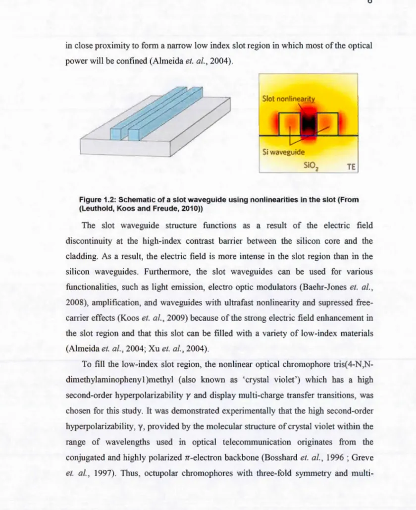
The design of integrated optical circuits requires the creation of optical waveguides. Thus, to put into context the work explained later in this thesis, an introduction to waveguide modes is presented. First, an ideal simple one dimensional optical waveguide (i.e. a slab waveguide) (see fig 2.1) is described to provide a basic understanding of how optical waveguides function and then the waveguide modes are derived using Maxwell 's equations.
xL:z
1
Cladd~ng n02• Core n1
y
T
Sub•trate n,Figure 2.1: Basis structure of a slab waveguide (From (Okamoto, 2010))
An optical waveguide has a core, a cladding and a substrate and it is uniform in at least one direction and able to direct light along an axis (see Fig. 2.1 ). The refractive index of the cladding n0 must be lower than that of the core n1 . The principle confining the light bearn into the waveguide structure can be understood as total internai reflection (TIR), which can be derived using Snell 's law.
Figure 2.2: The refractive indices of a strip waveguide. (From (Okamoto, 2010) For TIR, the following condition must be satisfied at the core-cladding interface (Okamoto, 2010):
n1 sin(rr/2 - ~) 2:
n
0 , (2.11)The relation between the incident angle(} and~ can be shown as: sin 8
=
n1sin(~)
:=:; jn12 -n
02
15
Hence, the critical condition for TIR is
() -- sm . -1
-\)nl
1
2-
no
2 -= () max• (2.13) A plane wave propagating along the z-direction bas phase fronts perpendicular to the light rays. The wavenumber and wavelength of light in the core are kn1 and Àjn1, respectively, where k=
2rr/
À
and À is the wavelength of light in vacuum. The propagation constants along y and x are given by (Okamoto, 201 0):f3
= kn1 cos<!> K = kn1 sin<!>(2.14) In arder ta obtain a guided mode, the condition for constructive interference must be satisfied and is given by the relation:
(2.15)
where m is integer. Equation (2.15) shows that the propagation angle of the light ray is discrete and is determined by the waveguide structure (core radius a, refractive index n1, refractive index difference 1:1 ). The optical field distribution that satisfies the phase-matching condition of Eq. (2.15) is called the mode.
2.1.3 Ideal Waveguide Mode Analysis
In integrated photonic circuits the waveguides usually support only a single mode (Radamson et Thylen, 2014). Hence modal analysis is an important aspect in the design process since it provides infonnation on the modes that propagate, their shapes and their propagation constants (Scarmozzino et. al., 2000). ln this section, the propagation characteristics of an ideal slab waveguide (see Fig. 2.1 ), which were explained based on simple ray tracing in section 2.1.2, are derived rigorously using wave analysis.
Maxwell's Eq. (2.1) and (2.2) in the frequency domain become two coupled differentiai equations for electric and magnetic fields:
_
aH
"ï/ xE= -110 -rat'
_ _ 2at
"ï/ x H- E0n
at'
(2.16) (2.17)If we consider a uniform refractive index profile in the z-direction, we will have
solutions in the following forms:
H
= H(x, y)ei(wt-{Jz),E
= E(x, y)ei(wt-{Jz),(2.18) (2.19)
The propagation constant, f3, is a function of the angular frequency w, a positive
(negative) value of f3 ( w) shows a propagation of the phase fronts in the positive
(negative) z-direction.
For each electromagnetic field components if we replace Eq. (2.16) and (2.17)
witb Eq. (2.16) and (2.17), we have:
aEz . . ay
+
tfJEy=
-tWfloHx aEz . . - ax - tfJEx=
-tWfloHy (2.20) aEy aEx . - - - = -tWfloHz ax ay aHz . - . 2 ay+
t/3Hy - tWEon Ex-a
Hz . - . 2 ax - tf3Hx - tWEon Ey (2.21) aHy a _ . 2 ax - ay - tWEon Ez.17
2.1.4 Modes in 3-0 Waveguides
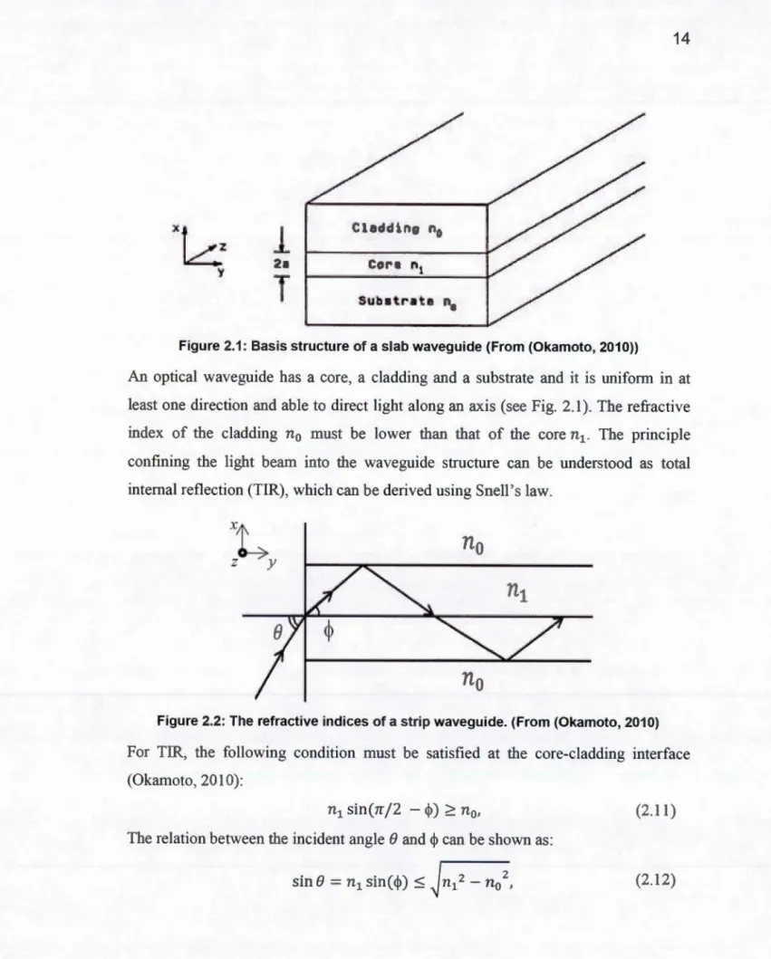
The electromagnetic field in strip waveguides (see Fig. 2.3) is concentrated in the core area and decays in the cladding region. The guided modes then split up into two
different polarization subsets: a dominant Ex-component called (quasi-)TE- modes and a dominant Ey-component called (quasi-) TM-polarized modes.
Two independent set of electromagnetic modes exist in strip waveguides, the transverse electric (TE) and transverse magnetic (TM) modes, which are the electromagnetic field distributions when the electric (for TE modes) or the magnetic
(for TM modes) field is situated in the plane and are perpendicular to the z-axis
(Okamoto, 2010). Moreover, a finite number of guided modes and a continuous
spectrum of radiation modes exist for a given waveguide at a fiXed frequency
w
andthey forrn a complete set ofEigenmodes (Marcuse, 1972).
A1r S1 nonhneanty
SiO TE
Figure 11.3: Schematic of a slot waveguide using nonlinearities in the slot (From
(Leuthold, Koos and Freude, 201 0))
The wave equation for TE mode is represented by (Okamoto, 2010):
d2E
_ _
Y+
(kznz - R2)E=
0dx
2 ~ Y ' where (2.22) (2.23)i
dEyH -
-z - Wflo dx ' (2.24)
Hy
=
Ez=
Ex=
O. (2.25)For TM mode, the wave equation is represented as:
!!__
(2_
dHy)+
(k
2 - {3 2 ) H =0
dx n2 dx n2 Y (2.26) where {3 Ex= 2 Ey, wE0n
(2.27)i
dHy Hz= -
wE 0n2 dx ' (2.28) Hz=
Hx=
Ey=
O. (2.29)There are several methods to calculate the mode profile of strip (also called channel) waveguides. The optical modes can be approximated with the effective index method or found more accurately with numerical methods.
Two popular numerical methods include: solving the two Maxwell curl equations in the frequency domain using Finite Difference in the Frequency Domain (FDTD)
(Fallahkhair, Li et. Murphy, 2008); and another one is called the finite-difference Bearn Propagation Method and it salves the scalar Helmholtz equations (Scarmozzino et. al., 2000).
2.1.5 Bearn Propagation Method (BPM) Technique
In this section the fundamental concept behind the Bearn Propagation Method or BPM (Feit and. Fleck Jr, 1978 ; Scarmozzino et. al., 2000) is described to fmd the optical modes of waveguides. BPM is a propagation teclmique for modeling ligbt propagation in integrated and fiber optic photonic deviees. It approximates the wave
19
methods as expressed in (Scannozzino et. al., 2000 ; Scarmozzino and Osgood Jr,
1991 ).
To solve the propagation problem, we need some basic k:nowledge about the
refractive index distribution, n(x, y, z) and the input wave field u(x, y, z = 0). The
algorithm requires additional numerical parameters including:
- A finite computational domain for x, y and z in the ranges (xmin' Xmax),
(Y min, Ymax) and (zmin' Zmax), respectively;
- The longitudinal step size, !J.z;
- The transverse grid sizes, !J.x and !J.y.
By considering the scalar field, thus neglecting polarization effects, we can write the
Helmholtz equation for monochromatic waves as:
az(/J az(/J az(/J
axz
+
ayz+
az2+
k(x, y, z)20=
0 (2.30) where the scalar electric field isE = ~(x,y, z)e-iwt
and the spatially dependentwavenumber k(x,y,z)
=
k0n(x,y,z) with k0=
2rrjÀ being the wavenumber in freespace.
In common guided-wave problems, there is a rapid phase variation m the
direction of propagation, which follows the guiding axis. This quick change in the
field ~ can often be ignored since it occurs on a time scale much shorter than the
changes due to modification in the deviee geometry. By introducing a slowly varying
field u, we can remove the rapid variation and simplify the problem:
~(x, y, z) = ueik:z (2.31)
where
k
is the reference wavenumber that represents the average phase variation ofthe field ~- If we substitute Eq. (2.31) into Eq. (2.30), we will have the following
equation for the slowly varying field (Scarmozzino et. al., 2000):
a
2u
.-a
u
a
2ua
2u 2 -zIf we assume that the variation of u in the z-direction is slow, the frrst term in Eq.
(2.32) can be neglected with respect to the second. The following equation is the
basic BPM equation in three dimensions:
au
i(à
2u
à
2u
2-z
)
àz
=
2k
àx2+
ày2+
(k - k )u (2.33)2.1.6 Third-order Nonlinear Interaction
In SOI based waveguides, the third-order nonlinear interaction can be realized by
two methods. The first way is the Self-phase modulation (SPM)/Cross-phase
modulation (XPM) caused by TPA and by the nonlinear interaction with the silicon
waveguide core (Dulkeith et. al., 2006; Tsang et. al., 2002; Yamada et. al., 2005).
Otherwise, the silicon core can be imbedded in a nonlinear cladding material and, as a result, an interaction with the transient section of the guided mode can be realized.
The intensity of third-order nonlinear interactions is represented by the nonlinear parameter.
In silicon the third-order nonlinearity can be represented by an electric field E
that bas three frequency components (wn):
3 3
E(r,t) =
I
En=~I(Ew
n
n(r,wn)e-iwnt
+c.e.), (2.34)n=l n=l
If we substitute Eq. (2.34) into Eq. (2. 7) and develop the frequency components
of xC3), we have new tenns for the third-order polarization, pC3), at new frequencies:
pC3)
=
~EoX
(
3)
[1Ew
11
2El+:.]
PM
- - - - -- - -- - -- - - -- -
-21
+
~
EoX(3)H
(E~l
Ewz ei(2wl +wz)t+
c. c.)+:.]
+
~
EoX(3)[~
(E~l E~z
ei(2wl-Wz)t+
c. c.)+:.]
HG
WM (2.35)
WM
WM
WM
where c.e. means the complex conjugate and the symbol :. denotes the possible permutations of frequencies. PM, HG and WG are phase modulation, harmonie generation and wave mixing, respectively. The nonlinear optical excitations are mentioned in Eq. (2.35) and between all these nonlinear processes only those which satisfies energy and momentum conservation (i.e. phase-matching) have efficient excitation (Boyd, 2008).
2.2
Nonlinear Parameters
In nonlinear optics, third-order materials have a profound impact and we can represent the properties of an optical media with a refractive index that depends on the intensity of the optical wave (I):
n
=
n0+
n2 /, (2.36)where
n
0 is the refractive index of the material and n2 represents the second-ardernonlinear refractive index that gives the ratio of the variation of the refractive index to the optical intensity (Boyd, 2008). This parameter is related to the third-order nonlinear susceptibility,
xC
3) by (Boyd, 2008):3
n
= x(3)2 4 2 1
which can be written in Gaussian units as
nz - = - - 1 07
x(
3)(esu) =x(
3)(esu) (cm2)
12rr
2 0.0395W
~c ~ (2.38)In general, in optical waveguides the core and the cover material have a third-order nonlinear susceptibility that can be considered to be nonzero and constant inside the interaction domain and that is zero outside of the nonlinear interaction domain. The interaction domain is defined as the region where the nonlinear materials and the optical field overlap.
Nonlinear effects are related to the intensity of the electromagnetic field in the medium. Moreover, the optical power can be obtained by integrating the intensity distribution over the optical waveguide cross section. If we consider a uniforrn distribution of intensity, 1, over an effective area, Aetf in a waveguide with a nonlinear interaction region, Dinter, we can express the intensity distribution from the power measured at the output of the waveguide, Pout as:
Pout
1=
-Aett• (2.39)
However, the field of an optical waveguide that bas been covered by a nonlinear material is unevenly distributed over the waveguide and within the core (Agrawal, 2013b ; Koos, 2007).
Thus, the two important quantities that can be used to study the nonlinear characteristics of a structure are the nonlinear Kerr parameter, n2 ( m2 /W), and the nonlinear waveguide parameter,
rcw-l
/m), which are defined as:- 3Zo (3) nz-4
no
zX '
(2.40) y =3WEol~
X(3) =2rr
~
4Aerrn6
ÀAerr'
(2.41) where Z0 is the impedance of free space and can be calculated with:23
(2.42)
and the effective area, Aetf is expressed by:
Z51JJ
Re{E(x,y)x
H*(x,y). ezdX dy}l2Aerr =
n6
ffiE(x,y)l4 dx dy (2.43)The nonlinear waveguide parameter, y, is maximised for strongly confmed modes (i.e. smallest nonlinear effective area, Aeff' and a large the nonlinear Kerr parameter (Foster, Mollet. Gaeta, 2004; Koos et. al., 2007).
2.3 Couple-Mode Theory of Four-Wave Mixing
2.3.1 Origin of Four Wave Mixing
Four-wave Mixing (FWM) is an optical process that originates from the third-order nonlinear susceptibility
xC
3). The FWM process is the nonlinear response of electrons from bound state to an electromagnetic field (Boyd, 2008) and its instantaneous nature makes its adequate for ultra-fast all-optical signal processing.This parametric process involves four optical waves, three optical signais at different frequencies (w1 , w2 , w3 ) and a fourth at a new frequency (w4 ). It obeys the law of conservation of energy and momentum, and it only becomes critical if the phase mismatch between the different signais is very small. When it occurs, energy passes from the pump and signais to the new frequency (idler), and thus, FWM can be used to perform wavelength conversion. The law of conservation of energy is expressed as (Agrawal, 2013a)
(2.44) The phase-matching condition for FWM is !::.k
=
0 and can be written as!J.k
=
(neff,3w3+
neff,4w4- neff,lwl- neft,zWz), where neff,m is the effective index at the frequency wi.(2.45) (2.46)
To initiate FWM, two pump beams should be launched at two frequencies w1
and w2 . In the the non-degenerate case, these two frequencies are not equal, w1
*
w2, but in the degenerate FWM case (DFWM) that occurs when a single pump bearn is present, the frequencies are equal, w1=
w2 and one must launch a strong purnp beam and a small signal into the waveguide to avoid the depletion of the pump. Thewaveguide medium interacts with the two beams and as a result it amplifies the signal
and creates an idler beam.
Degenerate FWM creates an idler wave at a frequency wi = 2wp- w5, in which wP, w5 and wi are the carrier frequencies of the pump, signal and idler wave,
respectively.
The corresponding mode fields for three frequencies, which are usually very similar, can be expressed as:
E(x,y) = E(x,y,wp) ~ E(x,y,w5 ) ~ E(x,y,wc),
H(x,y)
=
H(x,y,wp)::::: H(x,y,w5 ) ~ H(x,y,wc),2.3.2 Coupled-Mode Theory
(2.47) (2.48)
As mentioned before, the FWM process originates from the nonlinear polarization caused in the material, and since in this case we have multiple fields interacting, the
polarization of each individual field can be written in the form:
(2.49) where {371is the propagation constant in the z-direction. From here, the coupled amplitude equations can be solved in the general fonn (Boyd, 2008):
25
dEn _ J2wn (nl) - - - - P
dz
ne
n (2.50)where En is the field amplitude at frequency Wn and it is related to the intensity by
ln= ncE0
1Enl
2/2.
In the case of DFWM, the coup led differentiai equations for a strong pump and low
power signal can be written as (Agrawal, 2013b; Hansryd et. al., 2002 ; Lau et. al., 2011 ; Sharping et. al., 2001):
dEP _ 1 [ P ] . l
1 2
dz -
-2
alin+
f3TPA/p EP+
ty Ep Ep,dEs 1 s . 2
-
= --
2 [aun+
2f3TPA1p]Es+
2ty1Epl Esdz
+
yEP 2Eiexp(ib.kz),dE1 1 [ 1 ] . l
1
2
dz =
-2
alin+
2f3TPA/p Es+ 2ty Ep Es+
yEP 2 Eiexp(ib.kz),(2.51)
(2.52)
(2.53)
where f3TPA is the TP A at the pump wavelength, afïn, afin and afin are the linear
propagation loss coefficients of the pump, signal and idler, respectively; b.k
=
2yiEpl2- (2kp- ks- k1) is the phase mismatch which should be very small for
DFWM; kp, ks and k1 are the wavenumbers of the pump, signal and idler,
respectively; y = 2rrn2/ÀpAeff is the effective nonlinearity; n2 is the nonlinear
index coefficient; Àp is the pump wavelength; and Aetf is the effective area of the
propagating mode.
2.3.2.1 Wavelength Conversion
pOUt
The conversiOn efficiency, rJ, is defined as rJ = fdler and can be evaluated by
P
:
l1n
a
l
comparing the power of the signal at the input, P1~nal> to the power of the idler at
section 2.3.2, and assuming efficient phase-matching, the conversion efficiency for DFWM can be written as (Agrawal, 2013b):
1JDFWM =(Re {y}PpumpL)2 (2.54)
where Ppump is the pump power; L is the interaction length; and y is the nonlinear parameter (Agrawal, 2013b ; Hansryd el. al., 2002 ; Stolen and Bjorkholm, 1982). Recently, FWM based wavelength conversion experiments were done with SOI waveguides (Foster et. al., 2006 ; Kuo el. al., 2006) but the low conversion efficiency ~ -13 dB is a common problem in ali cases.
2.3.2.2 Chromatic Dispersion
Dispersion occurs when the phase velocity of a wave depends on its frequency and, more specifically, chromatic dispersion is the sum of material dispersion and waveguide dispersion. In other words, chromatic dispersion is the interaction of an electromagnetic wave with the bound electrons of a dielectric that depends on the frequency.
Wh en a wave goes through a dielectric medium with a refractive index of n, the light slows to a speed of c/n where c is the velocity of light in vacuum. The phase velocity of a wave, Vp =
w
/
k, is the velocity with which the phase of a wave propagates in a dielectric medium. However, when light is confined and propagates in a waveguide, the general defmition can be rewritten as:w
c
Vp= - =
-{3 neff (2.55)
where neff is the effective index of the guided mode, defined as neff = : 0
• The group velocity can be defined as the velocity at whicb energy and infonnation propagate along the wave and can be expressed as:
d{J
27
1 1 ( dnett) ng
fl1
= - =- ne11Cw)
+
w
- -
=-Vg
c
dwc
where ng is the group index Eq. (2.57) can be expressed in terms of À as:
dneff ng(À) = ne11 (À) - À~,
(2.57)
(2.58)
When an optical pulse travels through a waveguide, the group velocity dispersion
(GVD) causes pulse broadening and the parameter {32, which characterises the GVD,
can be defined as:
d2{3 1 dneff d2neff {32 = -d 2 = - (2 - d-
+
w d 2 )(JJ
c
(JJ (JJ(2.59)
The dispersion parameter, D, with respect to wavelength is represented as
df31 2rrc À d2neff
D = dÀ =
- 7
{32 = - c dÀ 2 (2.60)These parameters are critical in nonlinear processes because they define the
phase-matching condition in optical waveguides at non-degenerate frequencies.
2.4 Nonlinear Optical Slot Waveguides
A recent breakthrough in integrated optics is the demonstration of the slot waveguide
structure, whicb bas two strip waveguides with a high refractive index core material
brought close together to form a narrow slot of low index material. Maxwell's
equations for high-index-contrast interfaces express that the electric field (E) component of the quasi-TE mode must experience a large discontinuity where the
amplitude is much higher in the low-index side. The 'slot waveguide' structure
confines the light in the region with the lower refractive index (Almeida et. al., 2004).
This is the opposite of what happens in standard waveguides where the light is
confined in the high index core.
To put it differently, because of the high-index contrast at the two interfaces of
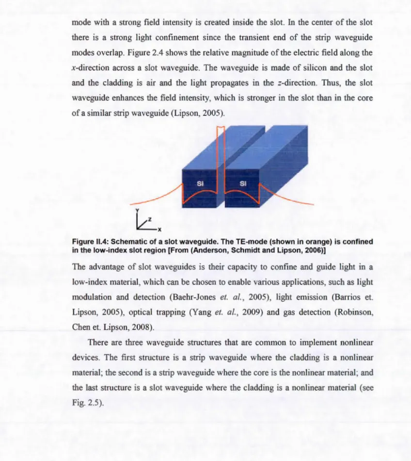
mode with a strong field intensity is created inside the slot. In the center of the slot there is a strong light confinement since the transient end of the strip waveguide modes overlap. Figure 2.4 shows the relative magnitude of the electric field along the x-direction across a slot waveguide. The waveguide is made of silicon and the slot and the cladding is air and the light propagates in the z-direction. Thus, the slot waveguide enhances the field intensity, which is stronger in the slot than in the core of a similar strip waveguide (Lipson, 2005).
Le_
xFigure 11.4: Schematic of a slot waveguide. The TE-mode (shown in orange) is confined
in the low-index slot region [From (Anderson, Schmidt and Lipson, 2006)]
The advantage of slot waveguides is their capacity to confine and guide light in a low-index material, which can be chosen to enable various applications, such as light modulation and detection (Baehr-Jones et. al., 2005), light emission (Barri os et. Lipson, 2005), optical trapping (Yang et. al., 2009) and gas detection (Robinson,
Chen et. Lipson, 2008).
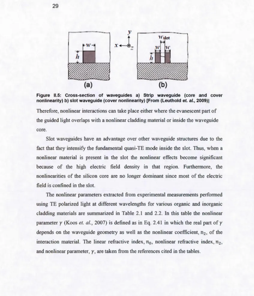
There are three waveguide structures that are common to implement nonlinear deviees. The first structure is a strip waveguide where the cladding is a nonlinear material; the second is a strip waveguide where the core is the nonlinear material; and the last structure is a slot waveguide where the cladding is a nonlinear material (see Fig. 2.5).
29
ll'slot
(a)
(b)
Figure 11.5: Cross-section of waveguides a) Strip waveguide (core and cover nonlinearity) b) slot waveguide (cover nonlinearity) [From (Leuthold et. al., 2009)]
Therefore, nonlinear interactions can take place either where the evanescent part of the guided light overlaps with a nonlinear cladding material or inside the waveguide core.
Slot waveguides have an advantage over other waveguide structures due to the fa ct that they intensify the fundamental quasi-TE mode inside the slot. Thus, wh en a nonlinear material is present in the slot the nonlinear effects become significant because of the high electric field density in that region. Furthermore, the nonlinearities of the silicon core are no longer dominant since most of the electric field is confined in the slot.
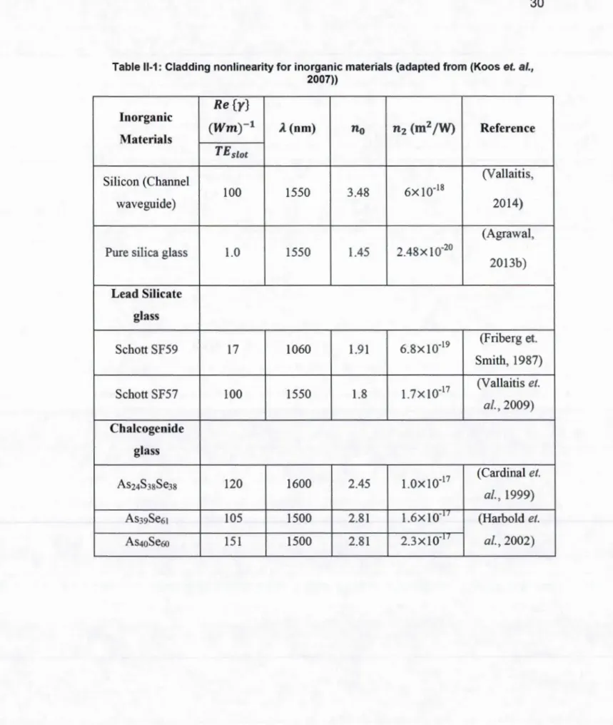
The nonlinear parameters extracted from experimental measurements performed using TE polarized light at different wavelengths for various organic and inorganic cladding materials are summarized in Table 2.1 and 2.2. In this table the nonlinear parameter y (Koos et. al., 2007) is defrned as in Eq. 2.41 in which the real part of y
depends on the waveguide geometry as weil as the nonlinear coefficient, n2, of the
interaction material. The linear refractive index,
n
0, nonlinear refractive index,n
2,Table 11-1: Cladding nonlinearity for inorganic materials (adapted from (Koos et. al., 2007))
Re
{y} Inorganic (Wm)-1 À(nm)nz
(m
2/W)
Referenceno
Materials TEslotSilicon (Channel (V allaitis,
100 1550 3.48 6x 10-18
waveguide) 2014)
(Agrawal,
Pure silica glass 1.0 1550 1.45 2.48x 1
o-
202013b) Lead Silicate glass Schott SF59 17 1060 1.91 6.8X 10⁻¹⁹ (Friberg et Smith, 1987) Schott SF57 100 1550 1.8 1.7X 10⁻¹⁷ (Vallaitis et. al., 2009) Chalcogenide glass
As24S3sSe3s 120 1600 2.45 l.Ox 10-17 (Cardinal et.
al., 1999)
As39Se61 105 1500 2.81 1.6x 1
o-
"
(Harbold et.As4oSe60 151 1500 2.81 2.3x10⁻¹
31
Table 11-2: Cladding nonlinearity for organic materials (adapted from (Koos et. al., 2007)) Re
{
y
}
Organic(W
m)-
1 À(nm)n
2(
m
2/
W)
Referencen
o
Materials TEslot (Rochford el. PDA 186 1319 ~1.5 4.8X 10"18 al., 1991 ; T ownsend el. al., 1988) (Gubler et. PTA 78 1907 1.5 2X 10"18 Bosshard, 2002) TEE 58 1907 1.5 1.sx w-~~ (Gubler, 2000) (Asobe el. al., PSTF66 109 1550 1.5 2.sxw
-
18 1995 ; Kaino, 2000) DANS 293 1319 1.57 8x 10"18 (Kim el. al., 1993) (Bhowmik et. PTS (PDA) 6950 1600 ~1.7 2.2xto-16 Thakur, 200 l ;Lawrence el. al., 1994)
In the first group of cladding materials presented, there are various glasses such as
lead silicate glasses and chalcogenide glasses that have high linear and nonlinear
refractive indices. Thus, the field enhancement in the slot decreases as a result of tbeir
high linear index (see Eq. 2.41). Accordingly, the effective area Aeff increases and