HAL Id: hal-03032030
https://hal.archives-ouvertes.fr/hal-03032030
Submitted on 30 Nov 2020
HAL is a multi-disciplinary open access
archive for the deposit and dissemination of
sci-entific research documents, whether they are
pub-lished or not. The documents may come from
teaching and research institutions in France or
abroad, or from public or private research centers.
L’archive ouverte pluridisciplinaire HAL, est
destinée au dépôt et à la diffusion de documents
scientifiques de niveau recherche, publiés ou non,
émanant des établissements d’enseignement et de
recherche français ou étrangers, des laboratoires
publics ou privés.
Strong Electron–Phonon Interaction in 2D Vertical
Homovalent III–V Singularities
Lipin Chen, Oliver Skibitzki, Laurent Pedesseau, Antoine Létoublon, Julie
Stervinou, Rozenn Bernard, Christophe Levallois, Rozenn Piron, Mathieu
Perrin, Markus Schubert, et al.
To cite this version:
Lipin Chen, Oliver Skibitzki, Laurent Pedesseau, Antoine Létoublon, Julie Stervinou, et al.. Strong
Electron–Phonon Interaction in 2D Vertical Homovalent III–V Singularities. ACS Nano, American
Chemical Society, 2020, 14 (10), pp.13127-13136. �10.1021/acsnano.0c04702�. �hal-03032030�
Strong Electron-Phonon Interaction in 2D Vertical Homovalent III-V
Singularities
Lipin Chen1, Oliver Skibitzki2, Laurent Pedesseau1, Antoine Létoublon1, Julie Stervinou1, Rozenn Bernard1, Christophe Levallois1, Rozenn Piron1, Mathieu Perrin1, Markus Andreas Schubert2, Alain Moréac3, Olivier Durand1,
Thomas Schroeder4, Nicolas Bertru1, Jacky Even1, Yoan Léger1, and Charles Cornet1*
1
Univ Rennes, INSA Rennes, CNRS, Institut FOTON-UMR 6082, F-35000 Rennes, France
2
IHP-Leibniz Institut fuer innovative Mikroelektronik, Im Technologiepark 25, 15236 Frankfurt /Oder
3
Univ Rennes, CNRS, IPR (Institut de Physique de Rennes) - UMR 6251, 35000, Rennes, France
4
Leibniz-Institut für Kristallzüchtung (IKZ) - Berlin, Germany
ABSTRACT:
Highly polar materials are usually preferred over weakly polar ones to study strong electron-phonon interactions and its fascinating properties. Here, we report on the achievement of simultaneous confinement of charge carriers and phonons at the vicinity of a 2D vertical homovalent singularity (antiphase boundary, (APB)) in an (In, Ga)P/SiGe/Si sample. The impact of the electron-phonon interaction on the photoluminescence processes is then clarified, by combining transmission electron microscopy, X-ray diffraction, ab initio calculations, Raman spectroscopy and photoluminescence experiments. 2D localization and layer group symmetry properties of homovalent electronic states and phonons are studied by first principles methods, leading to the prediction of a type II band alignment between the APB and the surrounding semiconductor matrix. A Huang-Rhys factor of 8 is finally experimentally determined for the APB emission line, underlining that a large and unusually strong electron-phonon coupling can be achieved by 2D vertical quantum confinement in an undoped III-V semiconductor. This work extends the concept of electron-phonon interaction to 2D vertically buried III-V homovalent nanoobjects and therefore provides different approaches for material designs, vertical carrier transport, heterostructure design on silicon and device applications with weakly polar semiconductors.
KEYWORDS: III-V semiconductor, 2D vertical homovalent singularity, carrier confinement, phonon confinement,
electron-phonon interaction
The electron-phonon interaction has a strong impact on electrical, optical and thermal properties of solids.1,2 Especially, strong electron-phonon interactions were recently investigated for materials and devices developments as well as for understanding of fundamental physical processes, such as phonon lasing,3 superconductivity,4 or colossal magnetoresistance.5 The strength of this interaction and the formation of a polaron however highly depends on the polarizability of the chemical bonds composing the material.6 Therefore, strong electron-phonon interaction was preferentially studied in highly polar materials, such as alkali halides,6 oxides,5,7 or perovskites.8 The strength of this
interaction is commonly quantified with the so-called Huang-Rhys factor S, whose maximum value may reach 100 with alkali halides.9 On the other hand, group-II-VI, III-V or IV semiconductors, have been widely used in photoelectric device applications due to their excellent optical and/or transport properties. When these bulk materials are pure and undoped, the electron-phonon interaction remains generally weak, reflected by quite low Huang-Rhys(S) factor (e.g. 0.0033 for InAs10 and 0.035 for CdSe11), as the chemical bonds are either covalent (group IV) or slightly polar (group III-V or II-VI). Effective enhancement of the electron-phonon interaction was successfully obtained by using spatial confinement or carrier localization effects.12 A. Alkauskas et al. comprehensively and deeply discussed the electron-phonon interaction in III-V semiconductors defects.13 Especially, punctual antisite defects were found to greatly enhance the electron-phonon interaction.14 M. Kang et al. discovered Holstein polaron in surface-doped layered MoS2 semiconductor.15 Electron-phonon coupling was also investigated in many different localized systems such as nanoscale core-shell structures,1 graphene and InAs double quantum dot (DQD) systems,16 WSe2/hBN heterostructure,2 or graphene/Monolayer h-BN structure.17
In this work, we demonstrate strong electron-phonon interactions in a 2D III-V singularity, which combines both phonon and charge carrier confinements. The nanostructure is composed of a vertical atomically-thin In-rich Indium gallium phosphide ((In,Ga)P) antiphase boundary (APB), where the homovalent bonds drastically change the local polarity and charge distribution in the crystal, leading to efficient phonon confinement and localized holes wavefunctions. It is furthermore surrounded by a Ga-rich (In,Ga)P barrier enabling the quantum confinement of carriers. The unusual electron-phonon coupling strength measured in these buried and non-oxidized III-V vertical singularities provides many perspectives to understand the physics of the electron-phonon interaction in semiconductors.
RESULTS AND DISCUSSION
APBs are commonly formed during the epitaxy of Zinc-Blende III-V semiconductors on a group IV substrate in the diamond phase (e.g. silicon (Si) or Germanium (Ge)). It originates from the two different ways for the III-V crystal to fit the group IV substrate orientation.18 As a consequence, two domains with different phases may grow on the same substrate, separated by wrong III-III or V-V bonds, inside the III-V matrix, as illustrated in Figure 1a. At first, APBs might be considered as detrimental non-radiative defects, comparable to grain boundaries in other polycrystalline materials. But we aim at demonstrating in the present work, that their topology is fundamentally different in nature, as they do not contain any dangling bonds, and respect the lattice ordering. The insertion of a local translational symmetry breaking, III-III(V-V) bond also adds 2 free holes (2 free electrons) in the semiconductor. However, unlike doping, APBs extend in the form of vertical 2D planes (at least locally), that can emerge at the sample surface. Theoretically, the APB composition may range from a pure vertical III-III APB to a pure V-V APB, resulting in these two extreme cases to a large excess of charges released in the lattice. But stoichiometric APBs (with equal numbers of III-III and V-V bonds within the same APB), as illustrated in Figure 1a, are more likely to form due to their relatively low formation energy resulting from the charge compensation effect.19
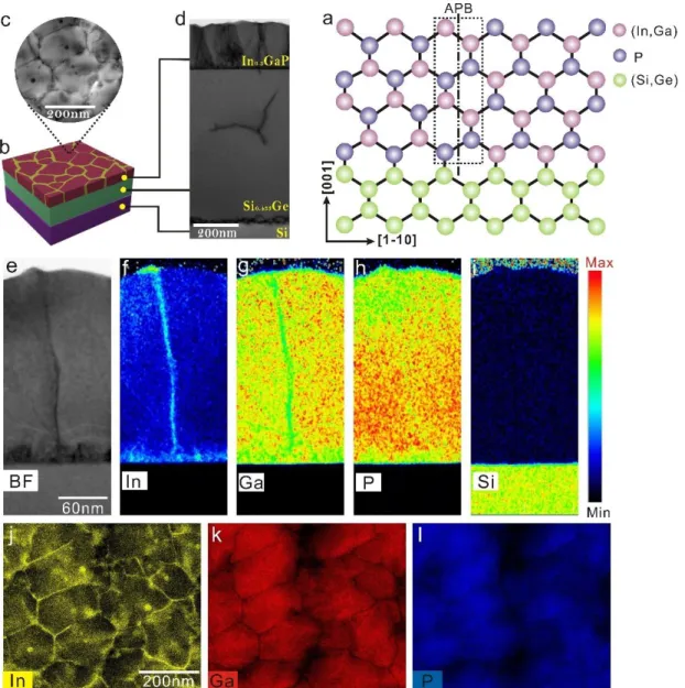
Figure 1. Structural characterizations of the InGaP/SiGe/Si sample. a, Sketch representing the atoms arrangement in an APB. b-d,Schematic image (b) as well as plan view (c) and cross-sectional (d) STEM images of the studied InGaP/SiGe/Si sample. e, Cross-sectional bright-field (BF) STEM image of the InGaP/SiGe/Si platform. The black line in the middle and the hump on the surface corresponds to the APB and surface nanostructure, respectively. f-i, Cross-sectional EDX elemental mapping images of indium(f), gallium (g), phosphorus(h) and silicon(i). j-l, Plan-view EDX mapping images of indium(j), gallium(k), phosphorus(l). Two kinds of In-rich nanostructures are observed: pure InP surface nanostructures and 2D In-rich vertical quantum wells (QWs) surrounding the APBsingularities.
Figure 1b is a schematic representation of the InGaP/SiGe/Si sample’s structure. Experimental scanning transmission electron microscopy (STEM) plan-view and cross-sectional images are shown in Figure 1c and Figure 1d, respectively. The sample is composed of three main layers: a Si substrate, a 760 nm-thick Si0.433Ge0.567 buffer layer and a 210 nm-thick InGaP III-V layer (Figure lb) with a nominal In content of 30%. The last epitaxial layer was grown at relatively high growth temperature (500°C) and low growth rate, to enhance non-equilibrium kinetic effects during the growth of the metastable (In, Ga)P alloy. Especially, In atoms are well-known for their ability to
efficiently migrate at the surface of InGaP semiconductors due to their low binding energy to the substrate. In this sample, APBs are propagating almost vertically until the surface (boundary between dark grey and clear grey in Figure 1d), giving rise to 2D vertical homovalent singularities. The 2D vertical homovalent singularities shown as random honeycomb-like lattice at the surface (black lines in Figure 1c) separate the different domains, as illustrated in Figure 1b.
Elemental mapping by an energy-dispersive X-ray (EDX) system in a scanning transmission electron microscope (STEM) was employed to analyze local chemical composition in the sample. Figure 1e presents the cross-sectional bright field image of the sample along the [110] direction. The black line in the middle represents one APB. Figure 1f-1i show the corresponding EDX mapping images of indium (Figure 1f), gallium (Figure 1g), phosphorus (Figure 1h), and silicon (Figure1i). Figure 1j-1l show the plane view EDX mapping images of indium (Figure 1j), gallium (Figure 1k), and phosphorus (Figure 1l). Additional STEM and EDX images are given in the supplementary materials (Figure S1 and Figure S2). First, almost pure InP surface quantum dots (QDs) are evidenced in Figure1c (black circular areas) and in Figure 1j, arising from demixion due to the non-equilibrium growth conditions used.20 Removal of these surface QDs will be discussed hereafter. Second, a preferential incorporation of In in the close vicinity of the antiphase boundary singularity is observed, together with an In-rich phase at the surface where the singularity emerges. Additionally, the use of X-Ray diffraction (see the supplementary materials), combined with EDX analysis allows the determination of In contents in the sample. The In composition inside the various domains (the largest part of the (In,Ga)P crystal) amounts to about 18%. On the contrary, it is hard to determine precisely the In content of the In-rich (In,Ga)P alloy close to the antiphase boundary singularity, but from EDX contrast, we deduce that the local content is larger than 60%, suggesting that the APB structures at the atomic scale are closer to InP-based APB rather than GaP-based APB. Finally, the In-rich phase observed at the vertical of the APB (where it emerges) is composed of pure InP. At the III-V/Si interface, intermixing is not observed. The origin of In accumulation at the APB level rather than Ga is therefore generally connected to the formation of an InP nanostructure at the surface where it emerges, to feed progressively the APB during the growth. In accumulation and InP nanostructure formation are the consequences of stress and electrostatic interactions induced at the surface where the APB emerges, and the favored migration of In atoms. A sketch of a possible growth mechanism consistent with these experimental observations is indicated in the supplementary information part (Figure S3). Overall, this preferential indium incorporation leads to the presence of a quantum confinement for carriers around the 2D homovalent singularities.
We demonstrate in the following, that the 2D homovalent APB singularities are interesting nano-objects with original optical, vibrational or electronic properties due to their very specific atomistic structure and the quantum confinement effects afforded by the surrounding In-rich local environment. For this purpose, we especially design a procedure to carefully remove the other nano-objects. Therefore, In-rich surface QDs were removed by Chemical Mechanical Polishing (CMP). The Scanning Electron Microscopy (SEM) measurement and Photoluminescence (PL) experiments performed before and after the CMP (Figure S4 and Figure S5) show the effective suppression of these surface nanostructures, including especially the disappearance of a low energy peak on the PL spectrum after CMP.
Figure 2. First principle simulations of electronic band structure and localized phonons for a model APB and experimental Raman spectrum a, The 32 atoms APB-supercell (APB in InP matrix) used for DFT band structure and phonon
calculations. b, Calculated electronic band structure of a 48 atoms APB-structure, weighted by the spatial localization of the wave functions at the APB interface. Layer group irreducible representations (IRs) at point are indicated. c, Partial charge density of the VBM and CBM at the Γ point for a 48 atoms supercell, integrated in the planes parallel to APBs. The dotted line corresponds to the APB plane. d, Phonon dispersions of 32 atoms APB-structure. The phonon modes highlighted by orange, blue, magenta, green and purple dotted lines correspond to additional localized modes related to APB planes. They are labelled according to layer group IRs at point. e,f,g, Partial vibrational (phonon) density of states of the middle InP atoms, In-In APB atoms and P-P APB atoms, corresponding to the atoms encircled by the black, red and green dotted lines respectively in Figure 2a.
h,i, Schematic images of vibration behaviors of the first Ag APB localized phonon mode around 5.3 THz and the Bu APB
localized phonon mode around 5.9 THz at Γ point according to layer group IRs, corresponding to the orange and blue dots in Figure 2d, respectively. j, Experimental Raman spectrum. The Raman peaks 2, 3, 4, 5, 6, 7, correspond respectively to Ge-Ge bonds, GaP transverse optical (TO) phonons, InP longitudinal optical (LO) phonons, GaP LO phonons, Ge-Si bonds and Si-Si bonds. The Raman peak 1 shows a good corresponding to the 5.3 THz phonon localized at the APB calculated previously. The inset shows the plane-view spatial distribution on the sample of the Raman peaks 1 (around 200cm-1, i.e. 6 THz) and 3.
As described previously, APBs are composed of III-III or V-V bonds,19,21 which induce a deficiency or excess of electrons. Therefore, it is expected to behave as acceptor or donor-like centers.19 One of the first consequences of the intrinsic APB structure is that inversion symmetry, which is absent in the bulk III-V zinc-blende lattice is restored locally (Figure 2a). This local structure entails specific symmetry properties as shown in the supplementary information part. In order to better understand and analyze the vibrational and electronic properties in the system, phonon and band structures need to be clarified. Phonon and electronic band structure calculations were performed using Density Functional Theory (DFT) for InP supercells containing two stoichiometric APB planes (called
hereafter APB-supercell) (Figure 2a). For comparison, the corresponding calculations were also done for a reference InP supercell structure without APB (called hereafter bulk-supercell) (Figure S8). A symmetry analysis was performed for the electronic states and phonon modes of APB supercells of various sizes at the point using the Pnnm space group or the p2/m11 layer group relevant respectively for the APB supercells or extrapolated for a single APB singularity (see supplementary information part).
Electronic bands were calculated along different k-paths (Z(0,0,0.5))-Г(0,0,0)-U(0.5,0,0.5); R(0.5,0.5,0.5)-Г(0,0,0)-S(0.5,0,0.5)), where the axis x, y, z of the reciprocal space correspond to the [001], [1-10], [110] crystallographic directions, based on Heyd–Scuseria–Ernzerhof (HSE) hybrid functional. The band structure plot of the APB-structure is shown in Figure 2b, where the states are weighted by their spatial localization at the APB plane. The color map from blue to red underlines the increase of localization effect of the states at the APB. Figure S9 shows the band structure of the reference bulk supercell with a direct band gap of 1.40eV. For a clear comparison, the Valence Band Maximum (VBM) and the Conduction Band Minimum (CBM) of the bulk-supercell were marked in Figure 2b, shown as the horizontal black dotted lines. Both structures show band folding effect due to the construction of the supercell. As compared to the bulk, the APB structure does not affect much the nature of the CBM while it introduces two localized states at the top of the VB, shifting the VBM upward (by roughly 0.5eV) and thus reducing the band gap. These 2D VB electronic states belong to Ag and Bg irreducible representation (IR) in a layer group representation (see supplementary part for more details). Figure 2c shows the planar averages of the partial charge densities of the VBM and CBM integrated parallel to the APB. The VBM partial charge density clearly reveals localization of carriers on the APB plane and the density drop between APBs, in good agreement with the weighted band structure represented in Figure 2b. Conversely, the charge density of CBM slightly decreases at the APB location, indicating an overall type-II band alignment between the APB singularity and the bulk (schematically shown in Figure 3c).
Phonon dispersions of the APB-supercell and the reference bulk-supercell (InP) are then computed and shown in Figure 2d and Figure S10, respectively, where R(0.5,0.5,0.5), Г(0,0,0) and U(0.5,0,0.5) are the high symmetry points of the first Brillouin zone. In both cases, the phonon dispersions also show band folding effects due to the construction of the supercell. From the known bulk phonon dispersions, we identify the contributions of underlying InP acoustic (low frequency) and optical (high frequency) phonon branches (see supplementary information for the illustration of band folding effects). We may notice that the computed bulk phonon frequencies are a little smaller than the experimental ones,22 which is an expected consequence of the generalized gradient approximation (GGA) that overestimates lattice constants and underestimates the energies of vibrational modes.23 Comparing the phonon dispersions of the bulk (Figure S10) and structure (Figure 2d), it can be clearly observed that the APB-supercell introduces several new flat phonon branches in the phonon dispersion gap, positioned at around 5.3THz, 5.9THz, 7.8THz, 8.0THz, 12.6THz, marked by orange, blue, magenta, green and purple dot lines, respectively (Figure 2d). These phonons correspond at the point respectively to the Ag, Bu, Au, Bu, Ag irreducible representations of the layer group for a single APB (see supplementary informations). Figure 2e-g show the partial vibrational density of states (PVDOS) of the “bulk-like” In-P bond, In-In APB bond and P-P APB bond (encircled by black, red and green dotted lines in Figure 2a), respectively, which reveals that the new flat phonon branches
mainly result from the APB singularity. Moreover, the localized phonon with relatively low frequency (around 5.3 THz) mainly comes from the vibration of the In-In APB bonds and the other localized phonons mainly correspond to the vibration of the P-P APB bonds. The vibration behavior of the five new phonon modes at the Γ point (corresponding to the orange, blue, magenta, green and purple dots in Figure 2d) were extracted. The corresponding movies were put in the supplementary material and the schematic images are shown in Figure 2h, Figure 2i, Figure S13a, Figure S13b and Figure S13c, respectively, where the arrows represent the vibration directions and amplitudes of the main atoms involved. We can see that the five new phonon modes are mainly localized at the APB plane singularity, which is consistent with the vibrational PVDOS calculated before.
Spatially- and spectrally-resolved Raman measurements were performed on the sample after CMP and the results are shown in Figure 2j. The Raman peaks 2, 3, 4, 5, 6, 7, correspond respectively to Ge-Ge bonds,24 GaP transverse optical (TO) phonons,25 InP longitudinal optical (LO) phonons,25 GaP LO phonons,25 Ge-Si bonds,24 and Si-Si bonds,24 and the InP TO phonons25 should give some contribution to the signal around 303cm-1. The Raman peak 1 is relatively broad and weak, but its central frequency (around 200cm-1, i.e. 6 THz) shows a reasonable agreement with the Ag Raman active mode with frequency around 5.3 THz localized at the APB calculated previously. In order to further confirm the contribution of the five localized phonons to the Raman signal, the Raman spectrum of the five localized phonons at point was calculated and extracted, shown in Figure S14. We thus confirm numerically that only the Ag localized phonons with frequency around 5.3 and 12.6 THz give a contribution to the Raman spectrum. Therefore, the Raman peak 1 in the experimental data is attributed to the Ag localized vibration with theoretical frequency around 5.3 THz. The Raman signal of the experimental data in the range of 400-500cm-1 should contain the contribution from the second Ag APB localized phonon with a theoretical frequency around 12.6 THz, but it is most probably hidden by the contributions related to the other parts of the sample. The hyperspectral mapping in the inset displays the spatial distribution of the Raman peak 3 of GaP TO (green area) and Raman peak 1 (red area) vibration modes. The clear observation of remaining red and green area in the spatial superposition of the two vibrational modes indicate that the two phonon vibrations do not originate from the same region. Based on the EDX images, we know that there are two main structures in the InGaP layer (after CMP): the main In-poor phase (InGaP with 18% In) and the In-rich phase located around the 2D APB singularities. Therefore, we attribute peak 3 observed in the Raman spectrum to lattice vibrations inside the In-poor domains away from the APB, while peak 1 comes from phonons localized at the APB homovalent singularities. The signature of the localized phonons (peak 1) in Raman experiments is relatively weak because of the small volume fraction of APBs. But this does not entail a low oscillator strength. Based on the structural investigations, the (band structure and phonon dispersion) calculations and Raman measurements, we can conclude that the 2D APB singularities simultaneously bring in both carrier and phonon localization in the same region of the sample, which are the basic ingredients to create uncommon carrier-phonon interaction effects. The existence of an unexpected low-frequency localized Raman-active optical mode at about 6 THz is in particular consistent with first-principles predictions.
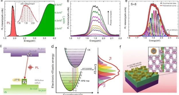
Temperature dependent (15300K) PL and room temperature ellipsometry measurements were performed on the sample after CMP. A Tauc-Lorentz model with two oscillators was used to fit the ellipsometry data (Figure S15a). The extracted refractive index (n), extinction coefficient (k) and absorption spectrum are shown in Figure S15b and
Figure S15c. The absorption spectrum was shifted at higher energy by 66 meV to account for the Varshni dependence of the bandgap.26 Therefore, low temperature absorption spectrum and PL are both given in Figure 3a. In the PL spectrum, one broad PL peak is observed between 1.8 and 2.1eV. In the absorption spectrum, one peak between 3.5 and 4.0eV can be observed, with a similar shape than the one usually reported for GaP,27 indicating that the absorption spectrum mainly comes from the In-poor phase. But the absorption curve starts from the high energy side of the PL around 2.1eV, which is smaller than the expected bandgap of the In-poor phase In0.18GaP at low temperature (which should be around 2.32eV).28 This absorption tail can result from the alloy fluctuation of InGaP matrix or another part of the material with a lower bandgap (i.e. the In-rich phase with the APB singularity).
Figure 3. Electron-phonon coupling. a, Photoluminescence and absorption spectra at low temperature (15K). The inset
corresponds to the PL spectrum in high magnification. b, Power-dependent Photoluminescence at 15 K. c,d, Mechanism of the Photoluminescence with a spatial representation (c) or within the electron-phonon interaction configuration coordinate point of view (d). e, Experimental data (grey dots) and theoretical fitting (red line) of the broad PL peak based on the Franck-Condon model. The small multicolored peaks correspond to the distinct phonon replicas contributions. f, Schematic plot of the 2D vertical In-rich structure, embedding APB planes with strong electron-phonon interaction.
Another important feature of the PL spectrum is the presence of several small peaks on the top (inset of Figure 3a), separated by approximately the same energy (24±2 meV, 5.8±0.5 THz, 193.6±16.1 cm-1), which shows the contribution of phonons in the PL process. The small peaks are referred to as phonon replicas. In fact, a phonon energy around 24 meV is much smaller than the optical phonons of both GaP and InP, while it is in fair agreement with the energy of phonons localized around APB planes, predicted theoretically and observed in Raman spectroscopy. The observation of these phonon replicas further shows that a specific PL signal results from the APB singularity region. Besides, the APB-localized phonons dispersion curves of Figure 2d are very flat, which can facilitate phonon-assisted emission.
(including small peaks and the broad contribution) remains proportionally unchanged with increasing pumping power, which further indicates the broad PL peak contains and only contains multi-phonon replicas. Figure S16 displays the logarithm plot of the integrated PL intensity versus excitation power and it shows super-linear to linear power dependency behavior, which is related to acceptor or donor-like effect of the APB29,30(for the details see the supplementary materials).
From the previous band structure calculations, the general mechanism of the PL resulting from the 2D homovalent singularity is schematically represented in Figure 3c. After illumination, the excited electrons in the conduction band recombine with the holes localized in the APB plane and leads to PL emission. This general picture is further confirmed by the temperature dependent PL shown in Figure S17, where the main activation energy found is 200 meV. This represents the detrapping of the localized holes in the APB 2D states to extended 3D states of the In-rich phase. The mechanisms of electron-phonon interaction leading to the phonon replicas in the PL spectrum are analyzed first following the simplified Franck-Condon approach (Figure 3d). The configuration coordinate diagram shows the potential well vs the normal mode coordinate (Q) and the dotted horizontal lines represent oscillator states.13 In this illustration, the potential well is ideally considered as harmonic so that the energy difference between two nearby oscillator states are the same and equal to the phonon energy.
Beyond the localization effect related to the 2D homovalent singularity itself, the APB is embedded in an In-rich region surrounded by In-poor regions, which further brings an additional quantum confinement effect. Therefore, we expect a large number of localized electrons at the vicinity of the singularity. During absorption of the laser pump, the incoming photons can excite the electrons into the conduction band (CB) and change the filling of the APB states. Based on the classical Franck-Condon approximation,31-33 this optical transition takes place instantaneously. Meanwhile, the ions are slow, and their position do not change when the electronic state changes. After losing the electrons, the lattice near the nanostucture relaxes to a new equilibrium position, through which the electrons relax to the bottom of the potential well of the conduction band of the 2D structure13 (the dotted green curves in Figure 3d). Then the excited electrons will recombine with the holes in different localized vibration states (v=0,1,2…), giving the photoluminescence, shown as the multicolor emission lines in Figure 3d, which correspond to the phonon replicas. The interaction between the electrons and phonons has usually to be strong to exhibit such quantum effects, which is consistent with the co-confinement of the electrons and phonons in the same region. The magenta emission line from the bottom of the conduction band potential well to the ground vibration state (=0) corresponds to the zero phonon line (ZPL). At low temperature, the photoluminescence intensity In of the n-th emission line follows the Poisson distribution:34
(1)
Where S is the Huang-Rhys factor which describes the magnitude of the electron-phonon coupling, and n the number of phonons generated in the transition. Moreover, the luminescence phonon wing is characterized by the relation: En=EZPL-nEph (EZPL and Eph corresponding to the energy position of the zero phonon emission line and the energy of phonon, respectively).
The broad PL was fitted based on the equation above. The phonon replicas were fitted by Gaussian functions with full width at half maximum (FWHM) of 26.5meV and a phonon energy of around 24 meV was used. Note that
Lorentzian functions did not allow to fit the phonon replicas correctly. The Gaussian broadening observed is mainly considered as the consequence of the inhomogeneous broadening effect due to the composition inhomogeneity or the different distances between the APBs.13 The broadening effect due to acoustic phonons shall amount only to a few meV range,35 which can be neglected in the present study. In addition, the energy difference between two nearby phonon lines in the low energy part of the spectrum becomes a bit smaller gradually, indicating that the potential well is slightly anharmonic. Anyway, this observation doesn’t impact the conclusions given here. Figure 3e shows the experimental data and the theoretical fitting achieved by the Franck-Condon principle. Accurate fitting of the experimental curve was only obtained with a S parameter of 8 and a ZPL at 2.097eV.
To our knowledge, a Huang-Rhys factor of 8 is considerably larger than those found usually for undoped bulk III-V and II-VI semiconductors, even with confinement of carriers such as in QDs or QWs (0.015 for InAs/GaAs QD;10 0.3 for InGaN/GaN QW;36 0.36-0.7 for CdSe QDs;371.25 for InP/GaInP QD38). It indicates the presence of unusual strong electron-phonon interaction in the 2D In-rich vertical singularity due to (i) the double quantum confinement by the vertical quantum well, and (ii) the simultaneous confinement of electrons and phonons in the same region (as shown in Figure 3f). In addition, time-resolved PL was measured and fitted by a model designed for type II band alignements39 (Figure S18). The good fitting and the observed long lifetime (within the µs order of magnitude) are consistent with the theoretical picture of a type II band alignment (as shown in Figure 3c). It indicates that confined holes in the APB play a major role in the enhancement of the electron-phonon interaction.
Finally, we shall discuss the possible microscopic origins of the observed strong coupling regime between localized carriers and phonons. Raman scattering measurements coupled with PL replica characterization and localized phonon simulations point toward a mechanism involving both 2D Ag even localized phonon modes and APB localized VB electronic states. Therefore, a specific optical deformation potential mechanism is the most probable process to explain the experimental observations.40 The observation of phonon replica is a signature of a strong electron-phonon interaction, which is consistent with the microscopic computation of a large electron phonon coupling matrix elements for the first localized non-polar Ag mode (vide infra). However, the second localized Ag mode is also predicted to exhibit a strong coupling to the same confined valence state, despite the absence of corresponding discrete signatures on top of the PL envelope. Therefore, other aspects beyond our theoretical description and simplified APB model structure are likely to be important as well, including phonon-phonon interactions or lattice disorder. The Raman scattering experiment (Figure 2j) indeed shows that the first low-frequency localized mode already exhibits a broader signature than extended lattice modes. We may thus infer that such broadening is even more important for the other localized modes, leading only to shallow contributions to the envelope of the PL spectrum. In addition, another classical electron-phonon coupling mechanism should be also considered for odd (polar) modes, that is the Fröhlich interaction. The theoretical study predicts that the APB polar phonon modes shall be located at a sizable energy above the lowest APB Ag even phonon mode, and therefore shall not be good candidates to explain the observed phonon replica. These localized polar modes are nevertheless likely to be coupled to localized VB electronic states.
Therefore, we rely on theoretical calculations to further investigate the electron-coupling processes induced by the new localized phonon modes around the APB structure. For that purpose, we calculated electron-phonon
interaction (EPI) matrix elements ( ) for both polar and non-polar-localized modes using state of the art DFT-based microscopic theory41-43 (for the complete definition of see the supplementary materials part). Table S4 lists the electron phonon interaction matrix elements | | related to the coupling at the point
between the Ag localized non-polar phonon modes and, the bottom of the conduction band (m=n=CBM) or the top of the valence band (m=n=VBM). We can find that the EPI matrix elements are large and consistent with a strong deformation potential interaction between the two Ag localized phonon modes and the localized VBM electronic state. On the other hand, Figure S19 shows the variation of the EPI matrix element for the polar-localized phonon modes as a function of q coupled to the same electronic states. Consistently with the symmetry analysis, the matrix elements vanish at the point (q=0). They may exhibit an increase at long wavelengths, q → 0 (Figure S19a), although these variations exhibit as well significant deviations from the classic analytical Fröhlich model (Figure S19b-d). More, the matrix elements correspond to sizeable numerical values (Figure S19) on the same order as the ones for non-polar modes at the point (Table S4), thereby suggesting that the coupling to the localized polar modes is important for optoelectronic properties, and also playing a role for hole transport. This can shed some light on the recent experimental observation of APBs benefiting to carrier transport at room temperature.44,45 Indeed, APBs are planar structures, not point defects and therefore, vertical transport in the APB planes can take place. In the present work, APBs can be assimilated to effective quantum wells forming planar conduction channels for carriers. Considering the recent researches that allow controlling both lateral and vertical extensions of APDs,18,46 more investigations are needed to characterize the nature and the strength of the electron-phonon interaction processes in such homovalent singularities.
CONCLUSION
In conclusion, the local change of chemical bonds polarity at the atomic scale in a weakly polar III-V crystal, positioned at the heart of a quantum confined vertical nanostructure enabled the simultaneous confinement of charge carriers and phonons at the vicinity of the 2D homovalent singularity. This situation led to a strong enhancement of the electron-phonon coupling, as testified by a large experimental Huang-Rhys factor and discussed in the framework of optical deformation potential and Fröhlich interaction. This extends the routes toward the understanding of electron-phonon interactions and gives different horizons for material designs or device applications with weakly polar semiconductors.
MATERIALS AND METHODS
Sample growth: The preparation of the studied In0.3GaP on SiGe/Si sample contains two main processes. The First step is the growth of a relaxed SiGe buffer layer on Si substrate.47 A 760nm Si0.433Ge0.567 layer was grown at 550°C and 80 Torr reactor pressure on one clean Si(001) wafer misoriented by 4o towards the [110] direction with a reduced pressure chemical vapor deposition (RPCVD) system. Then SiGe was annealed in-situ at 1000°C for 5 mins under H2 flow for relaxation. The second step is the regrowth of In0.3GaP on SiGe/Si pseudo-substrate, which contains two growth modes: Migration Enhanced Epitaxy (MEE) and traditional Molecular Beam Epitaxy (MBE). The first 10nm InGaP layer was grown with the MEE growth mode. One MEE cycle consists in a first 0.63ML Ga
deposition at a growth rate of 0.1ML/s, followed by a 0.27ML In deposition at the same growth rate (0.1ML/s), and then by a 4s growth interruption. Finally, a 200nm-thick In0.3GaP layer is grown at 500°C in the conventional continuous MBE growth mode and at a growth rate of 0.14ML/s on the MEE layer.
Experimental measurements: The Scanning Transmission Electron Microscopy (STEM) high-resolution imaging
and Energy Dispersive X-Spectroscopy (EDX) were obtained by FEI Tecnai Osiris TEM tool, operating at 200 kV with implemented energy-dispersive x-ray (EDX) detector. TEM lamellas were prepared by milling and undercutting processes using a Zeiss NVision 40 focused ion beam operating at up to 30 kV. The InGaP/SiGe/Si samples were characterized by X-ray diffraction (XRD) on a 4 circles Brucker D8 Diffractometer. A Bartels asymmetric Ge (220) monochromator was used for both line scans and reciprocal space maps. The detection is ensured by a LynxeyeTM, 1 dimensional position sensitive detector (PSD) allowing a collection angle of 2.6° over 2θ. 1% H3PO4 solution was used for the Chemical Mechanical Polishing (CMP). The SEM images were obtained by using a JEOL JSM-7100 scanning electron microscope. Ellipsometry measurements were performed at room temperature in the 1.5–5 eV photon energy region. To fit the measured ellipsometry spectra, a Tauc-Lorentz model including two oscillators was used to describe InGaP optical contants, and the SiGe buffer layer was considered as a known alloy. The power-dependent PL was designed with the excitation power from 24 mW to 0.24 mW at 15K by using a 405 nm laser. The temperature-dependent PL was performed from 15 K to 100 K through a helium bath closed cycle cryostat with an excitation density of 24 mW by using the 405 nm laser. The laser spot size of the 405 nm laser is around 10 μm on the sample. The time-resolved PL was measured at 15K by a Q-switched 355 nm pulse laser at an excitation intensity of 560 mW/cm2 (pulse duration:7ns, repetition rate:5kHz). The signals were filtered by two different bandpass filters of 600 and 800 nm. The fluorescence lifetime was determined by time-correlated single photon counting. Raman image was obtained with a HR800 micro-Raman spectrometer (HORIBA Scientific). The HR800 system is a high-resolution spectrometer fitted with a confocal microscopy system coupled to different lasers. Our experiments were performed in "confocal mode" with a 532 nm diode laser as excitation source and, to avoid sample heating, an optical density filter was used.
DFT calculations: Band structure and phonon calculations were performed with the density functional theory
(DFT)48 by combining the Vienna Ab initio Simulation package (VASP),49,50 VASPKIT package,51 and PHONOPY package52 codes. DFT calculations are performed using the plane-wave projector augmented wave (PAW) method53,54 as implemented in VASP code. The standard generalized gradient approximation (GGA) parameterized by Perdew-Burke-Ernzerhof (PBE)55 were used for structure optimization and phonon calculation, and the Heyd– Scuseria–Ernzerhof (HSE) hybrid functional56-58 was chosen for the band calculation, with energy cutoff of 500eV. A Monkhorst-Pack 4x1x6 grid59,60 of k points was set on the geometry optimization step and the structures were relaxed until the Hellmann-Feynman forces on the atoms were less than 10-4 eV/Å. The symmetry information and Raman spectrum of the localized phonons around APB were extracted through the phono3py61 package codes. The symmetry properties of electronic states were calculated and extracted based on metaGGA (TB-mBJ)62 potential by Quantum Espresso (QE)package codes.63,64 Electron-phonon interaction matrix element calculations based on the local-density approximation (LDA) and the Quantum Espresso (QE)code.42,43
ASSOCIATED CONTENT Supporting Information
The Supporting Information is available free of charge at …
Additional scanning transmission electron microscopy (STEM) images; Sketch of the APB vertical growth; Scanning electron microscopy (SEM) and Photoluminescence (PL) of the reported sample before and after chemical mechanical polishing; X-Ray diffraction and Reciprocal Space Mappings (RSM); Reference density functional theory calculations for bulk InP; Symmetry analysis of the APB supercell electronic and vibrational properties; Density functional theory computation of phonon modes localized on the APB; Ellipsometry measurements; Power-dependent photoluminescence experiments; Temperature-Power-dependent photoluminescence experiments; Time-resolved photoluminescence; Microscopic calculation of the electron-phonon interaction (EPI) matrix elements.
ACKNOWLEDGMENTS
This research was supported by the French National Research Agency ANTIPODE Project (Grant No. 14-CE26-0014-01), Région Bretagne. Lipin Chen acknowledges the China Scholarship Council (CSC) for her Ph.D financial support (No. 2017-6254). The authors acknowledge RENATECH (French Network of Major Technology Centers) within Nanorennes for technological support and thank the SIR platform of ScanMAT at University of Rennes 1 for technical assistance for the Raman measurements. DFT calculations were performed at Institut FOTON and the work was granted access to the HPC resources of TGCC/CINES/IDRIS under the allocation 2019-A0060906724 made by GENCI. Jacky Even acknowledges the financial support from the Institut Universitaire de France.
Author contributions
C. C. and Y. L. conceived the idea. C. C., O. S., R. B., N. B., designed and fabricated the samples. M. A. S., T. S. and O. S. performed and analyzed the STEM measurements. A. L., O. S. and L. C. did the X-Ray diffraction experiments and analysis. J. S. carried out the SEM experiments. L. C. and C. L. did the ellipsometry measurements and analyzed the data. C. C. and O. D. contributed to structural investigations analysis. Y. L., L. C. and R. P. did and analyzed PL experiments. A. M. performed the Raman experiments. J. E., L. C. and L. P. performed and analyzed the DFT calculations. M. P. contributed to phonon analysis. L. C. and J. E. performed the symmetry analysis. L. C., C. C., Y. L., L. P and J. E. clarified the physics of the phonon-electron interaction. L. C. and C. C. wrote and finalized the manuscript. All authors reviewed and commented on the manuscript.
Notes
The authors declare no competing financial interest.All images in figure graphics (including the TOC graphic) are original and created by the authors.
REFERENCES
(1) Yu, S.; Zhang, J.; Tang, Y.; Ouyang, M. Engineering Acoustic Phonons and Electron−Phonon Coupling by the Nanoscale Interface. Nano Lett. 2015, 15, 6282–6288.
(2) Jin, C.; Kim, J.; Suh, J.; Shi, Z.; Chen, B.; Fan, X.; Kam, M.; Watanabe, K.; Taniguchi, T.; Tongay, S. Interlayer Electron−Phonon Coupling in WSe2/HBN Heterostructures. Nat. Phys. 2017, 13, 127. (3) Czerniuk, T.; Brüggemann, C.; Tepper, J.; Brodbeck, S.; Schneider, C.; Kamp, M.; Höfling, S.; Glavin,
B. A.; Yakovlev, D. R.; Akimov, A. V.; Bayer, M. Lasing from Active Optomechanical Resonators. Nat. Commun. 2014, 5, 1–6.
(4) Lanzara, A.; Bogdanov, P. V.; Zhou, X. J.; Kellar, S. A.; Feng, D. L.; Lu, E. D.; Yoshida, T.; Eisaki, H.; Fujimori, A.; Kishio, K.; Shimoyama, J.-I.; Noda, T.; Uchida, S.; Hussain, Z.; Shen, Z.-X. Evidence for Ubiquitous Strong Electron-Phonon Coupling in High-Temperature Superconductors. Nature 2001, 412, 510–514.
(5) Driza, N.; Blanco-Canosa, S.; Bakr, M.; Soltan, S.; Khalid, M.; Mustafa, L.; Kawashima, K.; Christiani, G.; Habermeier, H.-U.; Khaliullin, G.; Ulrich, C.; Tacon, M. L.; Keimer, B. Long-Range Transfer of Electron−Phonon Coupling in Oxide Superlattices. Nat. Mater. 2012, 11, 675.
(6) Byrnes, S. J. F. Basic Theory and Phenomenology of Polarons; University of California: Berkeley, 2008.
(7) Wang, Z.; Walker, S. M.; Tamai, A.; Wang, Y.; Ristic, Z.; Bruno, F. Y.; Torre, A. de la; Riccò, S.; Plumb, N. C.; Shi, M.; Hlawenka, P.; Sánchez-Barriga, J.; Varykhalov, A.; Kim, T. K.; Hoesch, M.; King, P. D. C.; Meevasana, W.; Diebold, U.; Mesot, J.; Moritz, B.; Devereaux, T. P.; Radovic, M.; Baumberger, F. Tailoring the Nature and Strength of Electron−Phonon Interactions in the SrTiO3(001)
2D Electron Liquid. Nat. Mater. 2016, 15, 835.
(8) Wright, A. D.; Verdi, C.; Milot, R. L.; Eperon, G. E.; Pérez-Osorio, M. A.; Snaith, H. J.; Giustino, F.; Johnston, M. B.; Herz, L. M. Electron−Phonon Coupling in Hybrid Lead Halide Perovskites. Nat. Commun. 2016, 7, 11755.
(9) Leung, C. H.; Song, K. S. On the Luminescence Quenching of F Centres in Alkali Halides. Solid State Commun. 1980, 33, 907–910.
(10) Bissiri, M.; Baldassarri Höger von Högersthal, G.; Bhatti, A. S.; Capizzi, M.; Frova, A.; Frigeri, P.; Franchi, S. Optical Evidence of Polaron Interaction in InAs/GaAs Quantum Dots. Phys. Rev. B 2000, 62, 4642–4646.
(11) Gindele, F.; Hild, K.; Langbein, W.; Woggon, U. Phonon Interaction of Single Excitons and Biexcitons. Phys. Rev. B 1999, 60, R2157–R2160.
(12) Heitz, R.; Mukhametzhanov, I.; Stier, O.; Madhukar, A.; Bimberg, D. Enhanced Polar Exciton-LO-Phonon Interaction in Quantum Dots. Phys. Rev. Lett. 1999, 83, 4654–4657.
(13) Alkauskas, A.; McCluskey, M. D.; Van de Walle, C. G. Tutorial: Defects in Semiconductors−Combining Experiment and Theory. J. Appl. Phys. 2016, 119, 181101.
(14) Fockele, M.; Meyer, B. K.; Spaeth, J. M.; Heuken, M.; Heime, K. Arsenic Antisite Defects in AlxGa 1-xAs Observed by Luminescence-Detected Electron-Spin Resonance. Phys. Rev. B 1989, 40, 2001– 2004.
(15) Kang, M.; Jung, S. W.; Shin, W. J.; Sohn, Y.; Ryu, S. H.; Kim, T. K.; Hoesch, M.; Kim, K. S. Holstein Polaron in a Valley-Degenerate Two-Dimensional Semiconductor. Nat. Mater. 2018, 17, 676.
(16) Roulleau, P.; Baer, S.; Choi, T.; Molitor, F.; Güttinger, J.; Müller, T.; Dröscher, S.; Ensslin, K.; Ihn, T. Coherent Electron−Phonon Coupling in Tailored Quantum Systems. Nat. Commun. 2011, 2, 239. (17) Brar, V. W.; Jang, M. S.; Sherrott, M.; Kim, S.; Lopez, J. J.; Kim, L. B.; Choi, M.; Atwater, H. Hybrid
Surface-Phonon-Plasmon Polariton Modes in Graphene/Monolayer h-BN Heterostructures. Nano Lett.
2014, 14, 3876–3880.
(18) Lucci, I.; Charbonnier, S.; Pedesseau, L.; Vallet, M.; Cerutti, L.; Rodriguez, J.-B.; Tournié, E.; Bernard, R.; Létoublon, A.; Bertru, N.; Le Corre, A.; Rennesson, S.; Semond, F.; Patriarche, G.; Largeau, L.; Turban, P.; Ponchet, A.; Cornet, C. Universal Description of III-V/Si Epitaxial Growth Processes. Phys. Rev. Mater. 2018, 2, 060401.
(19) Rubel, O.; Baranovskii, S. Formation Energies of Antiphase Boundaries in GaAs and GaP: An ab Initio Study. Int. J. Mol. Sci. 2009, 10, 5104–5114.
(20) Yuan, Q.; Liang, B.; Zhou, C.; Wang, Y.; Guo, Y.; Wang, S.; Fu, G.; Mazur, Y. I.; Ware, M. E.; Salamo, G. J. Interplay Effect of Temperature and Excitation Intensity on the Photoluminescence Characteristics of InGaAs/GaAs Surface Quantum Dots. Nanoscale Res. Lett. 2018, 13, 387.
(21) Tea, E.; Vidal, J.; Pedesseau, L.; Cornet, C.; Jancu, J.-M.; Even, J.; Laribi, S.; Guillemoles, J.-F.; Durand, O. Theoretical Study of Optical Properties of Anti Phase Domains in GaP. J. Appl. Phys. 2014, 115, 063502.
(22) Lindsay, L.; Broido, D. A.; Reinecke, T. L. Ab Initio Thermal Transport in Compound Semiconductors. Phys. Rev. B 2013, 87, 165201.
(23) Haas, P.; Tran, F.; Blaha, P.; Schwarz, K. Construction of an Optimal GGA Functional for Molecules and Solids. Phys. Rev. B 2011, 83, 205117.
(24) Ravaux, F.; S. Rajput, N.; Abed, J.; George, L.; Tiner, M.; Jouiad, M. Effect of Rapid Thermal Annealing on Crystallization and Stress Relaxation of SiGe Nanoparticles Deposited by ICP PECVD. RSC Adv. 2017, 7, 32087–32092.
(25) Peternai, L.; Kováč, J.; Irmer, G.; Hasenöhrl, S.; Novák, J.; Srnánek, R. Investigation of Graded InxGa1−xP Buffer by Raman Scattering Method. Microelectron. J. 2006, 37, 487–490.
(26) Varshni, Y. P. Temperature Dependence of the Energy Gap in Semiconductors. Physica 1967, 34, 149– 154.
(27) Aspnes, D. E.; Studna, A. A. Dielectric Functions and Optical Parameters of Si, Ge, GaP, GaAs, GaSb, InP, InAs, and InSb from 1.5 to 6.0 EV. Phys. Rev. B 1983, 27, 985–1009.
(28) Zhang, Y.; Gu, Y. Al(Ga)InP-GaAs Photodiodes Tailored for Specific Wavelength Range. Photodiodes - Fundam. Appl. 2012.
(29) Bimberg, D.; Schairer, W.; Sondergeld, M.; Yep, T. O. Bound Exciton Luminescence in Epitaxial Sn-Doped Gallium-Arsenide. J. Lumin. 1970, 3, 175–184.
(30) Hellmann, R.; Euteneuer, A.; Hense, S. G.; Feldmann, J.; Thomas, P.; Göbel, E. O.; Yakovlev, D. R.; Waag, A.; Landwehr, G. Low-Temperature Anti-Stokes Luminescence Mediated by Disorder in Semiconductor Quantum-Well Structures. Phys. Rev. B 1995, 51, 18053–18056.
(31) Stoneham, A. M. Theory of Defects in Solids: Electronic Structure of Defects in Insulators and Semiconductors; Clarendon Press: Oxford, 2001.
(32) Lax, M. The Franck-Condon Principle and Its Application to Crystals. J. Chem. Phys. 1952, 20, 1752– 1760.
(33) Markham, J. J. Interaction of Normal Modes with Electron Traps. Rev. Mod. Phys. 1959, 31, 956–989. (34) Malm, H. L.; Haering, R. R. Franck-Condon Effects in the Luminescence of CdS. Can. J. Phys. 1971,
49, 2970–2988.
(35) Besombes, L.; Kheng, K.; Marsal, L.; Mariette, H. Acoustic Phonon Broadening Mechanism in Single Quantum Dot Emission. Phys. Rev. B 2001, 63, 155307.
(36) Paskov, P. P.; Holtz, P. O.; Monemar, B.; Kamiyama, S.; Iwaya, M.; Amano, H.; Akasaki, I. Phonon-Assisted Photoluminescence in InGaN/GaN Multiple Quantum Wells. Phys. Status Solidi B 2002, 234, 755–758.
(37) Norris, D. J.; Efros, Al. L.; Rosen, M.; Bawendi, M. G. Size Dependence of Exciton Fine Structure in CdSe Quantum Dots. Phys. Rev. B 1996, 53, 16347–16354.
(38) Odnoblyudov, M. A.; Yassievich, I. N.; Chao, K. A. Polaron Effects in Quantum Dots. Phys. Rev. Lett.
1999, 83, 4884–4887.
(39) Mourad, D.; Richters, J.-P.; Gérard, L.; André, R.; Bleuse, J.; Mariette, H. Determination of Valence-Band Offset at Cubic CdSe/ZnTe Type-II Heterojunctions: A Combined Experimental and Theoretical Approach. Phys. Rev. B 2012, 86, 195308.
(40) Braun, D.; Rühle, W. W.; Trallero-Giner, C.; Collet, J. Spectroscopic Determination of the Optical Deformation-Potential Constant in Semiconductors. Phys. Rev. Lett. 1991, 67, 2335.
(41) Giustino, F. Electron-Phonon Interactions from First Principles. Rev. Mod. Phys. 2017, 89, 015003. (42) Verdi, C.; Giustino, F. Fröhlich Electron-Phonon Vertex from First Principles. Phys. Rev. Lett. 2015,
(43) Poncé, S.; Giustino, F.; Margine, R.; Verdi, C. School on Electron−Phonon Physics from First Principles, http://indico.ictp.it/event/8301/session/96/contribution/534/material/0/ (accessed Aug 18, 2020).
(44) Cornet, C.; Da Silva, M.; Levallois, C.; Durand, O. Chapter 28 - GaP/Si-Based Photovoltaic Devices Grown by Molecular Beam Epitaxy. In Molecular Beam Epitaxy (Second Edition); Henini, M., Ed.; Elsevier: Amsterdam, 2018; pp 637–648.
(45) Alqahtani, M.; Sathasivam, S.; Chen, L.; Jurczak, P.; Piron, R.; Levallois, C.; Létoublon, A.; Léger, Y.; Boyer-Richard, S.; Bertru, N.; Jancu, J.-M.; Cornet, C.; Wu, J.; P. Parkin, I. Photoelectrochemical Water Oxidation of GaP1−xSbx with a Direct Band Gap of 1.65 EV for Full Spectrum Solar Energy Harvesting. Sustain. Energy Fuels 2019.
(46) Guillemé, P.; Vallet, M.; Stodolna, J.; Ponchet, A.; Cornet, C.; Létoublon, A.; Féron, P.; Durand, O.; Léger, Y.; Dumeige, Y. Antiphase Domain Tailoring for Combination of Modal and 4¯ -Quasi-Phase Matching in Gallium Phosphide Microdisks. Opt. Express 2016, 24, 14608–14617.
(47) Skibitzki, O.; Paszuk, A.; Hatami, F.; Zaumseil, P.; Yamamoto, Y.; Andreas Schubert, M.; Trampert, A.; Tillack, B.; Ted Masselink, W.; Hannappel, T.; Schroeder, T. Lattice-Engineered Si1-xGex-Buffer on Si(001) for GaP Integration. J. Appl. Phys. 2014, 115, 103501.
(48) Kohn, W.; Sham, L. J. Self-Consistent Equations including Exchange and Correlation Effects. Phys. Rev. 1965, 140, A1133–A1138.
(49) Kresse, G.; Furthmüller, J. Efficiency of Ab-Initio Total Energy Calculations for Metals and Semiconductors Using a Plane-Wave Basis Set. Comput. Mater. Sci. 1996, 6, 15–50.
(50) Kresse, G.; Furthmüller, J. Efficient Iterative Schemes for ab Initio Total-Energy Calculations Using a Plane-Wave Basis Set. Phys. Rev. B 1996, 54, 11169–11186.
(51) Wang, V.; Xu, N.; Liu, J. C.; Tang, G.; Geng, W.-T. VASPKIT: A Pre- and Post-Processing Program for VASP Code. ArXiv190808269 Cond-Mat 2020.
(52) Togo, A.; Tanaka, I. First Principles Phonon Calculations in Materials Science. Scr. Mater. 2015, 108, 1–5.
(53) Blöchl, P. E. Projector Augmented-Wave Method. Phys. Rev. B 1994, 50, 17953–17979.
(54) Kresse, G.; Joubert, D. From Ultrasoft Pseudopotentials to the Projector Augmented-Wave Method. Phys. Rev. B 1999, 59, 1758–1775.
(55) Perdew, J. P.; Burke, K.; Ernzerhof, M. Generalized Gradient Approximation Made Simple. Phys. Rev. Lett. 1996, 77, 3865–3868.
(56) Paier, J.; Marsman, M.; Hummer, K.; Kresse, G.; Gerber, I. C.; Ángyán, J. G. Screened Hybrid Density Functionals Applied to Solids. J. Chem. Phys. 2006, 124, 154709.
(57) Heyd, J.; Scuseria, G. E.; Ernzerhof, M. Hybrid Functionals Based on a Screened Coulomb Potential. J. Chem. Phys. 2003, 118, 8207–8215.
(58) Heyd, J.; Scuseria, G. E. Efficient Hybrid Density Functional Calculations in Solids: Assessment of the Heyd-Scuseria-Ernzerhof Screened Coulomb Hybrid Functional. J. Chem. Phys. 2004, 121, 1187– 1192.
(59) Monkhorst, H. J.; Pack, J. D. Special Points for Brillouin-Zone Integrations. Phys. Rev. B 1976, 13, 5188–5192.
(60) Pack, J. D.; Monkhorst, H. J. “Special Points for Brillouin-Zone Integrations”−A Reply. Phys. Rev. B
1977, 16, 1748–1749.
(61) Togo, A.; Chaput, L.; Tanaka, I. Distributions of Phonon Lifetimes in Brillouin Zones. Phys. Rev. B
2015, 91, 094306.
(62) Tran, F.; Blaha, P. Accurate Band Gaps of Semiconductors and Insulators with a Semilocal Exchange-Correlation Potential. Phys. Rev. Lett. 2009, 102, 226401.
(63) Giannozzi, P.; Baroni, S.; Bonini, N.; Calandra, M.; Car, R.; Cavazzoni, C.; Ceresoli, D.; Chiarotti, G. L.; Cococcioni, M.; Dabo, I.; Corso, A. D.; Gironcoli, S. de; Fabris, S.; Fratesi, G.; Gebauer, R.; Gerstmann, U.; Gougoussis, C.; Kokalj, A.; Lazzeri, M.; Martin-Samos, L. et al. A Modular and Open-Source Software Project for Quantum Simulations of Materials. J. Phys. Condens. Matter 2009, 21, 395502.
(64) Giannozzi, P.; Andreussi, O.; Brumme, T.; Bunau, O.; Nardelli, M. B.; Calandra, M.; Car, R.; Cavazzoni, C.; Ceresoli, D.; Cococcioni, M.; Colonna, N.; Carnimeo, I.; Corso, A. D.; Gironcoli, S. de; Delugas, P.; DiStasio, R. A.; Ferretti, A.; Floris, A.; Fratesi, G.; Fugallo, G. et al. Advanced Capabilities for Materials Modelling with Quantum ESPRESSO. J. Phys. Condens. Matter 2017, 29, 465901.