STRUCTURAL, OPTICAL AND ELECTRICAL PROPERTIES OF BULK CuIn0.7Ga0.3Se2 SEMICONDUCTOR COMPOUND
S. Gagui1, B. Hadjoudja2, B. Chouial3, B. Zaidi4 and A. Chibani5,*
Semiconductor Laboratory, Department of Physics, University of Badji Mokhtar, Annaba, Algeria
ABSTRACT
In this work, we report on the study of structural, electrical and optical properties of the
CuIn0.7Ga0.3Se2 compound. Analysis by X-ray diffraction showed that the prepared ingots are
polycrystalline and of chalcopyrite structure. The preferential orientation in the plane (112) which is very suitable for the photovoltaic conversion was obtained. On the other hand, the lattice parameters a and c were calculated from the X-ray spectra, the c/a ratio was found to be equal to 2. Measurements of the electrical properties permitted us to get 7,645 Ω cm for the
resistivity and 4,761.1016 cm-3 for the carrier concentration. Characterization by energy
dispersive spectrometer (EDS) of the prepared ingots, allowed us to infer that their chemical composition is quasi-stoichiometric. Absorption measurements were performed using a UV-VIS-NIR spectrophotometer and a value of 1.13 eV for the band gap width was obtained.
Keywords: CuIn0.7Ga0.3Se2; elaboration; characterization; photovoltaic conversion.
Author Correspondence, e-mail: Souheyla_gagui@yahoo.fr
1. INTRODUCTION
The production of electricity from solar cells requires the use of a photoconductive layer, said absorbent layer which converts the light radiation in electron-hole pairs, the created carriers are collected by performing a junction on the surface of the absorbent. For the photovoltaic conversion, silicon remains the most used material. However, in order to reduce the cost of solar modules, other materials, particularly those in polycrystalline thin films such as
Cu-III-VI2 compounds are currently the subject of many researches. With their high absorption
in the manufacture of solar cells. Indeed, the solar cells based on chalcopyrite structure materials have a number of advantages in the race to produce solar modules on a large scale.
In this regard, we are interested in the development and study of CuIn0.7Ga0.3Se2 compound
for the manufacture of solar cells.
2. EXPERIMENTAL CONDITIONS
CuIn0.7Ga0.3Se2 compound ingots were prepared by a technique based on the vertical
Bridgman method [1, 2]. We followed the following steps: placing the mixture of the four
elements (Cu, In, Ga, Se) in a quartz tube sealed under a high vacuum of 10-6 torr. A
temperature-resistant wire permits to introduce the tube into the furnace, and to place the mixture in the middle of the latter. The elements forming the mixture are in the form of grains with a consistent purity: 5N for copper and 6N and for indium, gallium and selenium. After sealing, the tube is placed in an oven where it is subject to a thermal cycle, which lasts 5 days. At the end of the cycle, we take out of the quartz tube from the furnace and retrieve the formed product.
The thermal cycle required for the preparation of the CuIn0.7Ga0.3Se2 compound comprises
seven steps (Figure 1).
Fig.1. Thermal Cycle for preparing the CuIn0.7Ga0.3Se2 compound
• Step 1: Heating up gradually from room temperature to 300 ° C.
60 300 Te m p er atu re [ °C ] 40 20 80 100 Fusion Heating Crystallization Cooling 1150 900 0 120 Time [h]
• Step 2: Flat level at 300 ° C for 5 hours. • Step 3: Heating up to 1150 ° C.
• Step 4: Fusion at 1150 ° C for 25 hours.
• Step 5: Crystallization between 1150 ° C and 900 ° C. • Step 6: Continued crystallization at 900 ° C for 10 hours. • Step 7: Slow cooling to room temperature.
The prepared sample has a good morphology with complete solidification. Figure 2 shows a
sample of CuIn0.7Ga0.3Se2 obtained by using the thermal cycle shown above.
Fig.2. CuIn0.7Ga0.3Se2 Sample showing complete solidification and good morphology
3. RESULTS AND DISCUSSION 3.1. Structural properties
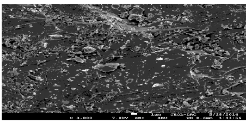
3.1.1. Morphology and chemical composition of the ingots
The prepared CuIn0.7Ga0.3Se2 ingots were characterized by EDS. The chemical composition of
Fig.3. SEM images of CuIn0.7Ga0.3Se2 ingot
The results reported in Table 1, show that the obtained CuIn0.7Ga0.3Se2 ingot is rich in copper.
Table 1. Chemical composition of ingot CuIn0.7Ga0.3Se2
3.1.2. X-ray characterization
Figure 4 shows the spectrum obtained by X-ray diffraction of CuIn0.7Ga0.3Se2 ingot. We
notice that the planes of orientation (112) and (204) have a high intensity with a preferred orientation along the direction (112). Similar results were reported by Suryanarayana et al. [3], which also indicated that the orientation planes (112) are desirable for photovoltaic conversion. Sample Cu (%) In (%) Ga (%) Se (%) Cu/(In+Ga) CuIn0.7Ga0.3Se2 25,83 19,98 4,72 49,47 1.04
Fig.4. XRD patterns of the CuIn0.7Ga0.3Se2 bulk
In addition to the planes of orientation (112), (103), (204), (116), (323) and (316) of the
ternary compound CuIn0.7Ga0.3Se2, most characteristic peaks of the chalcopyrite structure
(101 ), (211), (301) and (305) are shown by the spectrum of the sample obtained
CuIn0.7Ga0.3Se2. These various orientation planes also show that the prepared ingot is
polycrystalline.
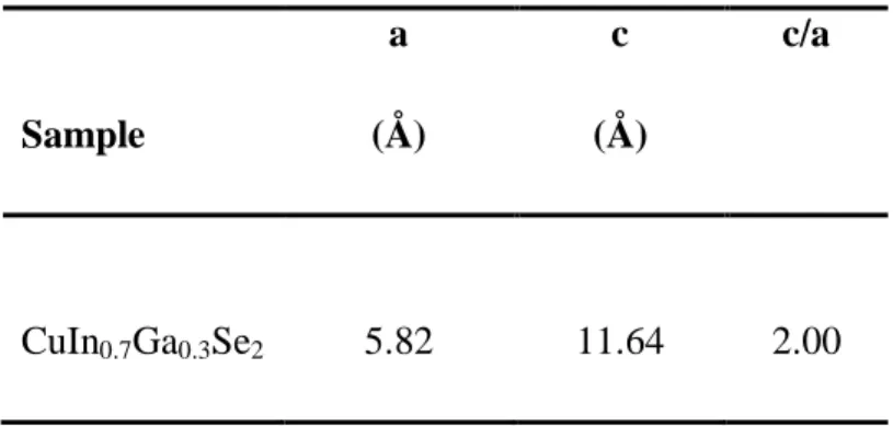
The obtained X-ray spectrum allowed us to calculate the lattice constants of CuIn0.7Ga0.3Se2
ingot, using the following equation:
2 2 2 2 2 2 c l a k h d 1
The values found are given in Table 2.
10 20 30 40 50 60 70 80 90 0 500 1000 1500 2000 2500 (3 0 7 ) (1 0 3 ) (5 0 1 ) (4 1 5 ) (3 0 5 ) (3 2 3 ) (3 0 1 ) (1 0 5 ) (2 1 3 ) (2 1 1 ) (1 0 1 ) (3 3 6 ) (4 2 4 ) (3 1 6 ) (1 1 6 ) (0 0 8 ) (2 0 4 ) (1 1 2 ) In te n si té (u .a ) 2 (deg)
Table 2. Lattice parameters “a”, “c” and c/a of the sample prepared CuIn0.7Ga0.3Se2
The presence of chalcopyrite structure characteristic peaks and the ratio of lattice constants
c/a = 2 show that the obtained CuIn0.7Ga0.3Se2 ingot has a chalcopyrite structure.
3.2. Electrical Properties
The electrical properties of CuIn0.7Ga0.3Se2 ingots were determined by Hall effect and
resistivity measurements at room temperature. The obtained values are reported in Table 3.
Table 3. Electrical characteristics of the prepared ingot CuIn0.7Ga0.3Se2
3.3. Optical properties
The optical properties were measured using a Cary 500 UV-VIS-NIR spectrophotometer in
the region of 250 nm to 1200 nm. Figure 5 shows the variation of (αhν) 2 as a function of (hv)
of the prepared CuIn0.7Ga0.3Se2 ingot. The gap value deduced by extrapolation of this curve
Sample a (Å) c (Å) c/a CuIn0.7Ga0.3Se2 5.82 11.64 2.00 Sample ρ (Ωcm) µ (cm2/vs) σ (1/Ωcm) Carriers concentration (cm-3) CuIn0.7Ga0.3Se2 7,645 17,15 0.1308 4,761.10+16
with the axis of the energy is Eg = 1.13 eV. Similar results have been reported by other authors [4-6].
Fig.5. Plot of (αhv)2 versus photon energy hν of CuIn0.7Ga0.3Se2 ingot
4. CONCLUSION
CuIn0.7Ga0.3Se2 ingots were prepared by a technique based on the vertical Bridgman method.
The obtained results showed that these ingots are polycrystalline and of chalcopyrite structure. The preferential orientation in the (112) plane was obtained., The lattice parameters a and c were calculated from the X-ray spectra, the c / a ratio was found to be equal to 2. The
obtained resistivity and carrier concentration were 7,645 Ωcm, and 4,761.1016
cm- 3
respectively. The gap of the obtained CuIn0.7Ga0.3Se2 ingot was found to be equal to 1.13 eV.
5. REFERENCES
[1] H. Du, C. H. Champness, I. Shih and T. Cheung, Thin Solid Films, vol. 480-481, p.42, (2005).
[2] W. S. Yip, I. Shih and C. H. Champness, J. Cryst. Growth, vol. 129, p.102, (1993). [3] C. Suryanarayana, Journal of materials science letters, vol. 20, p 2179 – 2181, (2001). [4] A. Bouloufa, K.Djessas, D.Todorovic, Materials Science in Semiconductor Processing, vol. 12, p 82 – 87, (2009). 1,0 1,5 2,0 2,5 3,0 0 5 10 15 20 h ) 2 (1 0 8 eV 2 /cm 2 )
Photon energie h (eV)
[5] F. B. Dejene, V. Alberts, J Phys D: Appl Phys,vol.38, p 22, (2005).
[6] K. Ramanathan, M.A. Contreras, C.L. Perkins, S. Asher, S.F. Hasoon, J. Keane, D. Young, M. Romero, W. Metzger, R. Noufi, J. Ward, A. Duda, Prog. Photovolt: Res. Appl,